Basic Terminology
- Control Unit - A control unit (CU) handles all processor control signals. It directs all input and output flow, fetches the code for instructions and controlling how data moves around the system.
- Arithmetic and Logic Unit (ALU) - The arithmetic logic unit is that part of the CPU that handles all the calculations the CPU may need, e.g. Addition, Subtraction, Comparisons. It performs Logical Operations, Bit Shifting Operations, and Arithmetic Operation.
 Figure - Basic CPU structure, illustrating ALU
 - Main Memory Unit (Registers) -
- Accumulator: Stores the results of calculations made by ALU.
- Program Counter (PC): Keeps track of the memory location of the next instructions to be dealt with. The PC then passes this next address to Memory Address Register (MAR).
- Memory Address Register (MAR): It stores the memory locations of instructions that need to be fetched from memory or stored into memory.
- Memory Data Register (MDR): It stores instructions fetched from memory or any data that is to be transferred to, and stored in, memory.
- Current Instruction Register (CIR): It stores the most recently fetched instructions while it is waiting to be coded and executed.
- Instruction Buffer Register (IBR): The instruction that is not to be executed immediately is placed in the instruction buffer register IBR.
- Input/Output Devices - Program or data is read into main memory from the input device or secondary storage under the control of CPU input instruction. Output devices are used to output the information from a computer.
- Buses - Data is transmitted from one part of a computer to another, connecting all major internal components to the CPU and memory, by the means of Buses. Types:
- Data Bus: It carries data among the memory unit, the I/O devices, and the processor.
- Address Bus: It carries the address of data (not the actual data) between memory and processor.
- Control Bus: It carries control commands from the CPU (and status signals from other devices) in order to control and coordinate all the activities within the computer.
Types of Computer Architecture
1. Von Neumann Architecture
- It uses one memory to store both the program instructions and the data.
- The CPU fetches instructions and data from the same place, one after another.
- This design is simpler and used in most traditional computers.
2. Harvard Architecture
- It uses two separate memories: one for program instructions and another for data.
- The CPU can fetch instructions and data at the same time, making it faster.
- This design is used in modern systems like embedded processors.
Instruction Set and Addressing Modes
A instruction is of various length depending upon the number of addresses it contain. Generally CPU organization are of three types on the basis of number of address fields:
- Single Accumulator organization
- General register organization
- Stack organization

Read more about Instruction Format, Here.
Basic Machine Instructions in COA
Machine instructions are the basic commands given to the processor to perform tasks. They operate directly on the hardware.
Types of Machine Instructions
- Data Transfer Instructions
- Move data between memory, registers, or I/O devices.
- Example:
LOAD, STORE, MOVE.
- Arithmetic Instructions
- Perform arithmetic operations like addition, subtraction, multiplication, and division.
- Example:
ADD, SUB, MUL, DIV.
- Logical Instructions
- Perform logical operations such as AND, OR, NOT, XOR.
- Example:
AND, OR, NOT, XOR.
- Control Transfer Instructions
- Change the sequence of execution (jump, branch, or call).
- Example:
JUMP, CALL, RET.
- Input/Output Instructions
- Allow communication between the processor and external devices.
- Example:
IN, OUT.
- Shift and Rotate Instructions
- Shift or rotate bits in a register.
- Example:
SHL (Shift Left), SHR (Shift Right), ROL (Rotate Left), ROR (Rotate Right).
Components of an Instruction
- Opcode: Specifies the operation to perform (e.g., ADD, SUB).
- Operands: Data to be operated on (e.g., registers, memory locations).
Addressing Modes

The addressing mode specifies a rule for interpreting or modifying the address field of the instruction before the operand is actually executed. An assembly language program instruction consists of two parts :

| Addressing Mode | Description | Example |
|---|
| Immediate Addressing | The operand is directly given in the instruction. | ADD R1, 5 (Add 5 to R1) |
| Register Addressing | The operand is stored in a register. | ADD R1, R2 (Add R2 to R1) |
| Direct Addressing | The operand is in memory, and the memory address is specified directly in the instruction. | LOAD R1, 1000 (Load data from memory address 1000 into R1) |
| Indirect Addressing | The address of the operand is stored in a register or memory location, not directly in the instruction. | LOAD R1, (R2) (Load data from the memory address stored in R2 into R1) |
| Register Indirect | Similar to indirect addressing, but specifically uses registers to hold the address of the operand. | LOAD R1, (R3) (Use R3 as pointer) |
| Indexed Addressing | The operand's address is calculated by adding an index (offset) to a base address stored in a register. | LOAD R1, 1000(R2) (Load data from memory address 1000 + R2 into R1) |
| Base Addressing | The base address is stored in a register, and the operand's offset is specified in the instruction. | LOAD R1, 200(RB) (RB = Base Register) |
| Relative Addressing | The operand's address is determined by adding an offset to the current program counter (PC). | JUMP 200 (Jump to PC + 200) |
| Implicit Addressing | The operand is implied by the instruction itself (no explicit address or operand). | CLR (Clear accumulator) |
Effective address or Offset: An offset is determined by adding any combination of three address elements: displacement, base and index.
Read more about Addressing Modes, Here.
RISC vs CISC
| RISC | CISC |
|---|
| Focus on software | Focus on hardware |
| Uses only Hardwired control unit | Uses both hardwired and microprogrammed control unit |
| Transistors are used for more registers | Transistors are used for storing complex
Instructions |
| Fixed sized instructions | Variable sized instructions |
| Can perform only Register to Register Arithmetic operations | Can perform REG to REG or REG to MEM or MEM to MEM |
| Requires more number of registers | Requires less number of registers |
| Code size is large | Code size is small |
| An instruction executed in a single clock cycle | Instruction takes more than one clock cycle |
| An instruction fit in one word. | Instructions are larger than the size of one word |
| Simple and limited addressing modes. | Complex and more addressing modes. |
| RISC is Reduced Instruction Cycle. | CISC is Complex Instruction Cycle. |
| The number of instructions are less as compared to CISC. | The number of instructions are more as compared to RISC. |
| It consumes the low power. | It consumes more/high power. |
| RISC is highly pipelined. | CISC is less pipelined. |
| RISC required more RAM . | CISC required less RAM. |
| Here, Addressing modes are less. | Here, Addressing modes are more. |
Read more about RISC vs CISC, Here.
CPU Registers
The instruction cycle involves multiple registers in the CPU to fetch, decode, execute and store results.
- Program Counter (PC)
- Holds the address of the next instruction to be executed.
- Updates after each instruction fetch.
- Instruction Register (IR)
- Stores the currently fetched instruction.
- Used by the control unit for decoding.
- Memory Address Register (MAR)
- Holds the memory address of the data or instruction to be fetched or stored.
- Memory Data Register (MDR) (or Memory Buffer Register, MBR)
- Temporarily holds the data being transferred to/from memory.
- Accumulator (AC)
- Stores intermediate arithmetic and logic results during execution.
- General Purpose Registers (GPR)
- Temporary storage for operands, results, or data during execution.
- Temporary Register (TR)
- Stores intermediate data during complex operations or instruction execution.
- Status Register / Flag Register
- Stores condition flags (e.g., zero, carry, overflow) to indicate the result of operations.
- Stack Pointer (SP)
- Points to the top of the stack in memory, used during function calls or interrupts.

Flag Registers
Status Flags
- Zero Flag (Z): When an arithmetic operation results in zero, the flip-flop called the Zero flag - which is set to one.
- Carry flag (CY): After an addition of two numbers, if the sum in the accumulator is larger than eight bits, then the flip-flop uses to indicate a carry called the Carry flag, which is set to one.
- Parity (P): If the result has an even number of 1s, the flag is set to 1; for an odd number of 1s the flag is reset.
- Auxiliary Carry (AC): In an arithmetic operation, when a carry is generated from lower nibble and passed on to higher nibble then this register is set to 1.
- Sign flag(S): It is a single bit in a system status (flag) register used to indicate whether the result of the last mathematical operation resulted in a value in which the most significant bit was set.
Instruction Cycle
1. Fetch: The CPU retrieves the next instruction from memory using the Program Counter (PC).
2. Indirect: If the instruction uses an indirect addressing mode, the effective memory address of the operand is resolved. Example: For LOAD R1, (100), the CPU fetches the address stored at memory location 100.
3. Execute: The CPU performs the operation specified by the instruction (e.g., arithmetic, logical, control).
4. Interrupt: If an interrupt request occurs (e.g., hardware interrupt or software exception), the CPU temporarily halts the current execution to service the interrupt. After servicing, the CPU resumes the instruction cycle.
Standard Instruction Cycle
This includes the basic steps for executing instructions:
- Fetch: Retrieve the instruction from memory.
- Decode: Identify the operation and operands.
- Execute: Perform the operation.
- Store (Write Back): Save the result (if any).
Read more about Instruction Cycle, Here.
Control Unit

The Control Unit (CU) is a core component of the CPU that directs its operation by generating control signals. It manages the execution of instructions by coordinating with the ALU, registers, and memory.
Types of Control Units
Hardwired Control Unit -
- Fixed logic circuits that correspond directly to the Boolean expressions are used to generate the control signals.
- Hardwired control is faster than micro-programmed control.
- A controller that uses this approach can operate at high speed.
- RISC architecture is based on hardwired control unit.
Micro-programmed Control Unit -
- The control signals associated with operations are stored in special memory units inaccessible by the programmer as Control Words.
- Control signals are generated by a program are similar to machine language programs.
- Micro-programmed control unit is slower in speed because of the time it takes to fetch microinstructions from the control memory.
- There are two type Micro-programmed control Unit:
- Horizontal Micro-programmed control Unit- The control signals are represented in the decoded binary format that is 1 bit/CS.
- Vertical Micro-programmed control Unit - The control signals re represented in the encoded binary format. For N control signals- Logn(N) bits are required.
Read more about Hardwired CU vs Micro-programmed CU, Here.
Microprogram: Program stored in memory that generates all control signals required to execute the instruction set correctly, it consists micro-instructions.
Micro-instruction: Contains a sequencing word and a control word. The control word is all control information required for one clock cycle.
Micro-operations: Micro-operations are the atomic operations which executes a particular micro-instruction. Example of micro-operation during the fetch cycle:
t1: MAR ←(PC)
t2: MBR ←Memory
    PC ←(PC) + I
t3: IR ←(MBR)
Memory Organization
- Memories are made up of registers.
- Each register in the memory is one storage location.
- The storage location is also called a memory location.
- Memory locations are identified using Address.
- The total number of bit a memory can store is its capacity.
| Byte Addressable Memory | Word Addressable Memory |
|---|
| When the data space in the cell = 8 bits then the corresponding address space is called as Byte Address. | When the data space in the cell = word length of CPU then the corresponding address space is called as Word Address. |
| Based on this data storage i.e. Bytewise storage, the memory chip configuration is named as Byte Addressable Memory. | Based on this data storage i.e. Wordwise storage, the memory chip configuration is named as Word Addressable Memory. |
Memory Hierarchy

Simultaneous access memory organization: If H1 and H2 are the Hit Ratios and T1 and T2 are the access time of L1 and L2 memory levels respectively then the
Average Memory Access Time can be calculated as:
T=(H1*T1)+((1-H1)*H2*T2
Hierarchical Access Memory Organization: If H1 and H2 are the Hit Ratios and T1 and T2 are the access time of L1 and L2 memory levels respectively then
Average Memory Access Time can be calculated as:
T=(H1*T1)+((1-H1)*H2*(T1+T2)
Read more about Simultaneous and Hierarchical Access Memory Organization, Here.
Cache Memory
Cache Memory is a special very high-speed memory. It is used to speed up and synchronizing with high-speed CPU. Levels of memory: Level 1 or Register, Level 2 or Cache memory, Level 3 or Main Memory, Level 4 or Secondary Memory.
Hit ratio = hit / (hit + miss) = no. of hits/total accesses
Locality of reference - Since size of cache memory is less as compared to main memory. So to check which part of main memory should be given priority and loaded in the cache is decided based on the locality of reference.
Types of Locality of reference
- Spatial Locality of reference: Spatial locality means instruction or data near to the current memory location that is being fetched, may be needed soon in the near future.
- Temporal Locality of reference: Temporal locality means current data or instruction that is being fetched may be needed soon. So we should store that data or instruction in the cache memory to avoid searching again in main memory for the same data.
- Cache Mapping: There are three different types of mapping used for the purpose of cache memory which is as follows: Direct mapping, Associative mapping and Set-Associative mapping.
Direct Mapping - Maps each block of main memory into only one possible cache line. If a line is previously taken up by a memory block and a new block needs to be loaded, the old block is trashed. An address space is split into two parts index field and a tag field. The cache is used to store the tag field whereas the rest is stored in the main memory.
Cache Line Number = Main Memory block Number % Number of Blocks in Cache
Associative Mapping - A block of main memory can map to any line of the cache that is freely available at that moment. The word offset bits are used to identify which word in the block is needed, all of the remaining bits become Tag.
Set-Associative Mapping - Cache lines are grouped into sets where each set contains k number of lines and a particular block of main memory can map to only one particular set of the cache. However, within that set, the memory block can map to any freely available cache line.
Cache Set Number = Main Memory block number % Number of sets in cache
Note: Translation Lookaside Buffer (i.e. TLB) is required only if Virtual Memory is used by a processor. In short, TLB speeds up the translation of virtual address to a physical address by storing page-table in faster memory. In fact, TLB also sits between the CPU and Main memory.
Read more about Cache Mapping Techniques, Here.
Multilevel Cache
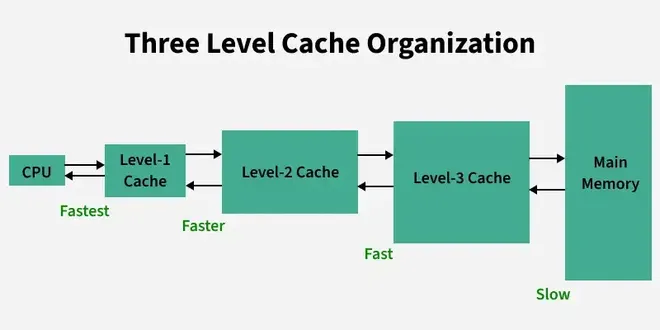 Multilevel Cache
Multilevel Caching is used in modern processors to improve memory access speed by introducing multiple levels of cache memory.
Types of Cache Levels
- L1 Cache (Level 1):
- Smallest, fastest, and closest to the CPU.
- Usually divided into Instruction Cache and Data Cache.
- L2 Cache (Level 2):
- Larger and slower than L1 but still faster than main memory.
- Acts as a bridge between L1 and L3/main memory.
- L3 Cache (Level 3):
- Shared across multiple cores.
- Larger and slower than L2 but faster than main memory.
Performance Metrics
- Hit Ratio:Percentage of memory accesses satisfied by the cache. \text{Hit Ratio} = \frac{\text{Cache Hits}}{\text{Total Accesses}}
- Miss Ratio: Percentage of memory accesses that result in a miss. \text{Miss Ratio} = 1 - \text{Hit Ratio}
Effective Memory Access Time (EMAT)
For 2-level cache:
\text{EMAT} = H_1 \times T_1 + (1 - H_1) \times [H_2 \times T_2 + (1 - H_2) \times T_M]- H1,H2H_1, H_2: Hit ratios for L1 and L2 caches.
- T1,T2T_1, T_2: Access times for L1 and L2 caches.
- TMT_M: Access time for main memory.
Cache Replacement Policies Table
| Algorithm | Key Idea |
|---|
| LRU | Replace least recently used block |
| FIFO | Replace oldest block |
| Random | Replace random block |
| LFU | Replace least-used block |
| Optimal | Replace block not used longest |
Cache Updation Policy
Write Through: In this technique, all write operations are made to main memory as well as to the cache, ensuring that main memory is always valid.
For hierarchical access: T_{read} = H \times T_{cache} + (1-H) \times (T_{cache} + T_{memory\_block}) \newline= T_{cache} + (1-H) \times T_{memory\_block}
For simultaneous access : T_{read} = H \times T_{cache} + (1-H) \times (T_{memory\_block}) \newlineT_{write} = T_{memory\_word}
Write Back: In write-back updates are made only in the cache. When an update occurs, a dirty bit, or use bit, associated with the line is set. Then, when a block is replaced, it is written back to main memory if and only if the dirty bit is set.
For hierarchical access: T_{read} = T_{write} = H \times T_{cache} + (1-H) \times (T_{cache} + T_{memory\_block} + T_{write\_back}) \\= T_{cache} + (1-H) \times (T_{memory\_block} + T_{write\_back}), \\ \text{ where } T_{write\_back} = x \times T_{memory\_block}, \text{ where } x \text{ is the fraction of dirty blocks}
For simultaneous access : T_{read} = T_{write} = H \times T_{cache} + (1-H) \times ( T_{memory\_block} + T_{write\_back}), \\ \text{ where } T_{write\_back} = x \times T_{memory\_block}, \text{ where } x \text{ is the fraction of dirty blocks}
Read more about Cache Memory, Here.
Cache Miss
| Type of Miss | Reason |
|---|
| Compulsory Miss | First-time access to data |
| Conflict Miss | Multiple blocks mapped to same cache line |
| Capacity Miss | Cache cannot hold all required data |
Read about Types of Cache Miss, Here.
I/O Interface
- An I/O (Input/Output) Interface connects the CPU and memory with external devices like keyboards, monitors, printers, etc.
- It acts as a bridge between the CPU and I/O devices to ensure smooth data transfer.
Data transfer between the main memory and I/o device may be handled in a variety of modes like :
Programmed I/O: In Programmed I/O, the CPU controls data transfer between the I/O device and memory without allowing direct access for the device. The I/O device sends one byte at a time, placing the data on the I/O bus and enabling the data valid line. The interface stores the byte in its data register, activates the data accepted line, and sets a flag bit to notify the CPU. The I/O device waits for the data accepted line to reset before sending the next byte. This process is managed step-by-step by the CPU, making it slower but synchronized.
Interrupt driven I/O: In interrupt driven I/O, the processor issues an I/O command, continues to execute other instructions, and is interrupted by the I/O module when the I/O module completes its work.
Read more about Interrupt, Here.
Interrupt Handling Techniques
- Daisy Chaining in Interrupts
Daisy chaining is a method of handling multiple interrupts in a system by connecting the devices in a serial or chain-like manner. When an interrupt request is generated, the priority is determined by the position of the device in the chain. The device closer to the CPU has higher priority. The interrupt signal travels through the chain, and each device checks if it is the source of the interrupt. If not, it passes the signal to the next device in the chain. This approach is simple to implement but suffers from longer delays for devices farther down the chain and is unsuitable for systems requiring precise or equal priority handling.
- Parallel Priority Interrupt
Parallel priority interrupts use a priority encoder to handle multiple interrupt requests simultaneously. All devices send their interrupt requests in parallel to the encoder, which determines the highest-priority interrupt and sends it to the CPU. This method is faster and more efficient than daisy chaining because it does not rely on signal propagation through a chain. Each device is assigned a priority, and the encoder ensures that the device with the highest priority gets serviced first. Parallel priority interrupts are commonly used in systems where speed and fair priority handling are essential.
Direct Memory Access(DMA): In Direct Memory Access (DMA), the I/O module and main memory exchange data directly without processor involvement.
Modes of DMA Transfer
1. Burst Mode (Block Transfer Mode)
In burst mode, the DMA controller takes full control of the system bus and transfers an entire block of data in one go before releasing the bus back to the CPU. This method is fast but can cause the CPU to be idle during the transfer, as it doesn't get access to the bus until the transfer is complete.
2. Cycle Stealing Mode
In cycle stealing mode, the DMA controller takes control of the bus for one data transfer (one word or one byte) at a time and then releases it back to the CPU. This allows the CPU and DMA to share the bus alternately, improving overall system efficiency while slightly slowing the DMA transfer.
Read more about Modes of DMA Transfer, Here.
| Mode | Key Feature | CPU Involvement | Use Case |
|---|
| Programmed I/O | CPU waits for device (polling) | High | Slow devices |
| Interrupt I/O | Device signals CPU via interrupt | Medium | Keyboards, printers |
| DMA | DMA controller handles transfer | Low (only initiation) | High-speed or bulk data devices |
DMA Controller
The DMA (Direct Memory Access) Controller is a hardware component that manages data transfer between memory and I/O devices without constant CPU involvement. It communicates with the CPU, memory, and I/O devices through control and data lines.
The CPU interacts with the DMA controller by selecting its registers via the address bus while enabling the DS (Data Select) and RS (Register Select) inputs. When the CPU grants the bus to the DMA (indicated by BG = 1, Bus Grant), the DMA takes control of the buses. The DMA then directly communicates with memory by placing the memory address on the address bus and activating the RD (Read) or WR (Write) control signals to perform data transfer.
The DMA controller communicates with external I/O devices using request and acknowledge lines:
- The I/O device sends a request signal when it needs to transfer data.
- The DMA acknowledges this request, initiates the data transfer, and ensures synchronization.
This process enables efficient and high-speed data transfer while freeing the CPU to perform other tasks.
Read more about I/O Interface, Here.
Pipelining
- Pipelining is a process of arrangement of hardware elements of the CPU such that its overall performance is increased.
- Simultaneous execution of more than one instruction takes place in a pipelined processor.
- RISC processor has 5 stage instruction pipeline to execute all the instructions in the RISC instruction set. Following are the 5 stages of RISC pipeline with their respective operations:
- Stage 1 (Instruction Fetch) In this stage the CPU reads instructions from the address in the memory whose value is present in the program counter.
- Stage 2 (Instruction Decode) In this stage, instruction is decoded and the register file is accessed to get the values from the registers used in the instruction.
- Stage 3 (Instruction Execute) In this stage, ALU operations are performed.
- Stage 4 (Memory Access) In this stage, memory operands are read and written from/to the memory that is present in the instruction.
- Stage 5 (Write Back) In this stage, computed/fetched value is written back to the register present in the instructions.
 5 stages of pipeline
Performance of a pipelined processor
Consider a 'k' segment/stages pipeline with clock cycle time as 'Tp'. Let there be 'n' tasks to be completed in the pipelined processor. So, time taken to execute 'n' instructions in a pipelined processor:
ETpipeline = k + n – 1 cycles
= (k + n – 1) Tp
In the same case, for a non-pipelined processor, execution time of 'n' instructions will be:
ETnon-pipeline = n * k * Tp
So, speedup (S) of the pipelined processor over non-pipelined processor, when 'n' tasks are executed on the same processor is:
S = Performance of pipelined processor / Performance of Non-pipelined processor
As the performance of a processor is inversely proportional to the execution time, we have:
S = ETnon-pipeline / ETpipeline
=> S = [n * k * Tp] / [(k + n – 1) * Tp]
S = [n * k] / [k + n – 1]
When the number of tasks 'n' are significantly larger than k, that is, n >> k
S = n * k / n
S = k
where 'k' are the number of stages in the pipeline. Also,
Efficiency = Given speed up / Max speed up = S / Smax
We know that, Smax = k So,
Efficiency = S / k
Throughput = Number of instructions / Total time to complete the instructions So,
Throughput = n / (k + n – 1) * Tp
Note: The cycles per instruction (CPI) value of an ideal pipelined processor is 1
Performance of pipeline with stalls
Speed Up (S) = CPInon-pipeline/ (1 + Number of stalls per instruction)
Read more about Pipelining, Here.
Dependencies and Data Hazard
There are mainly three types of dependencies possible in a pipelined processor. These are :
Structural dependency:
- This dependency arises due to the resource conflict in the pipeline. A resource conflict is a situation when more than one instruction tries to access the same resource in the same cycle. A resource can be a register, memory, or ALU.
- To minimize structural dependency stalls in the pipeline, we use a hardware mechanism called Renaming.
Control Dependency:
- This type of dependency occurs during the transfer of control instructions such as BRANCH, CALL, JMP, etc. On many instruction architectures, the processor will not know the target address of these instructions when it needs to insert the new instruction into the pipeline. Due to this, unwanted instructions are fed to the pipeline.
- Branch Prediction is the method through which stalls due to control dependency can be eliminated. In this at 1st stage prediction is done about which branch will be taken.
Data Dependency :
- Data dependency occurs when one instruction depends on the result of another instruction. It can cause data hazards in pipelined processors.
Types of Hazards in Pipelined Processors
Hazards are situations that cause the pipeline to stall or delay instruction execution. There are three main types of hazards:
1. Structural Hazards
- Occur when hardware resources are insufficient to handle the current instruction stream.
- Example: If only one memory unit exists, and both instruction fetch and data access need it simultaneously.
Solution:
- Add more resources (e.g., separate instruction and data memory – Harvard architecture).
- Use scheduling to avoid conflicts.
2. Data Hazards
- Arise when an instruction depends on data from a previous instruction that has not yet completed.
Types of Data Hazards:
- RAW (Read After Write): True dependency.
- WAR (Write After Read): Anti-dependency.
- WAW (Write After Write): Output dependency.
Solution:
- Data forwarding/bypassing.
- Insert pipeline stalls (NOPs).
- Instruction scheduling.
3. Control Hazards
- Occur due to branch or jump instructions, where the next instruction to execute is uncertain until the branch is resolved.
Solution:
- Branch prediction techniques.
- Delayed branching (use NOPs).
- Dynamic scheduling.
Read more about Dependencies and Hazards, Here.
IEEE Standard 754 Floating Point Numbers
There are several ways to represent floating point number but IEEE 754 is the most efficient in most cases. IEEE 754 has 3 basic components:
The Sign of Mantissa - This is as simple as the name. 0 represents a positive number while 1 represents a negative number.
The Biased exponent - The exponent field needs to represent both positive and negative exponents. A bias is added to the actual exponent in order to get the stored exponent.
The Normalised Mantisa - The mantissa is part of a number in scientific notation or a floating-point number, consisting of its significant digits. Here we have only 2 digits, i.e. O and 1. So a normalised mantissa is one with only one 1 to the left of the decimal.
The IEEE 754 Standard is used to represent floating-point numbers in binary. It has two formats:
- Single Precision (32-bit)
- Double Precision (64-bit)
 IEEE 754 Floating Point Standard
E=0,M=0: Zero
Read more about IEEE Floating Point Notation, Here.
Similar Reads
Computer Organization and Architecture Tutorial In this Computer Organization and Architecture Tutorial, you’ll learn all the basic to advanced concepts like pipelining, microprogrammed control, computer architecture, instruction design, and format. Computer Organization and Architecture is used to design computer systems. Computer architecture I
5 min read
Basic Computer Instructions
What is a Computer?A computer is an electronic device that processes, stores, and executes instructions to perform tasks. It includes key components such as the CPU (Central Processing Unit), RAM (Memory), storage (HDD/SSD), input devices (keyboard, mouse), output devices (monitor, printer), and peripherals (USB drive
13 min read
Issues in Computer DesignComputer Design is the structure in which components relate to each other. The designer deals with a particular level of system at a time and there are different types of issues at different levels. At each level, the designer is concerned with the structure and function. The structure is the skelet
3 min read
Difference between assembly language and high level languageProgramming Language is categorized into assembly language and high-level language. Assembly-level language is a low-level language that is understandable by machines whereas High-level language is human-understandable language. What is Assembly Language?It is a low-level language that allows users
2 min read
Addressing ModesAddressing modes are the techniques used by the CPU to identify where the data needed for an operation is stored. They provide rules for interpreting or modifying the address field in an instruction before accessing the operand.Addressing modes for 8086 instructions are divided into two categories:
7 min read
Difference between Memory based and Register based Addressing ModesPrerequisite - Addressing Modes Addressing modes are the operations field specifies the operations which need to be performed. The operation must be executed on some data which is already stored in computer registers or in the memory. The way of choosing operands during program execution is dependen
4 min read
Computer Organization - Von Neumann architectureComputer Organization is like understanding the "blueprint" of how a computer works internally. One of the most important models in this field is the Von Neumann architecture, which is the foundation of most modern computers. Named after John von Neumann, this architecture introduced the concept of
6 min read
Harvard ArchitectureIn a normal computer that follows von Neumann architecture, instructions, and data both are stored in the same memory. So same buses are used to fetch instructions and data. This means the CPU cannot do both things together (read the instruction and read/write data). So, to overcome this problem, Ha
5 min read
Interaction of a Program with HardwareWhen a Programmer writes a program, it is fed into the computer and how does it actually work? So, this article is about the process of how the program code that is written on any text editor is fed to the computer and gets executed. As we all know computers work with only two numbers,i.e. 0s or 1s.
3 min read
Simplified Instructional Computer (SIC)Simplified Instructional Computer (SIC) is a hypothetical computer that has hardware features that are often found in real machines. There are two versions of this machine: SIC standard ModelSIC/XE(extra equipment or expensive)Object programs for SIC can be properly executed on SIC/XE which is known
4 min read
Instruction Set used in simplified instructional Computer (SIC)Prerequisite - Simplified Instructional Computer (SIC) These are the instructions used in programming the Simplified Instructional Computer(SIC). Here, A stands for Accumulator M stands for Memory CC stands for Condition Code PC stands for Program Counter RMB stands for Right Most Byte L stands for
1 min read
Instruction Set used in SIC/XEPre-Requisite: SIC/XE Architecture SIC/XE (Simplified Instructional Computer Extra Equipment or Extra Expensive). SIC/XE is an advanced version of SIC. Both SIC and SIC/XE are closely related to each other that’s why they are Upward Compatible. Below mentioned are the instructions that are used in S
2 min read
RISC and CISC in Computer OrganizationRISC is the way to make hardware simpler whereas CISC is the single instruction that handles multiple work. In this article, we are going to discuss RISC and CISC in detail as well as the Difference between RISC and CISC, Let's proceed with RISC first. Reduced Instruction Set Architecture (RISC) The
5 min read
Vector processor classificationVector processors have rightfully come into prominence when it comes to designing computing architecture by virtue of how they handle large datasets efficiently. A large portion of this efficiency is due to the retrieval from architectural configurations used in the implementation. Vector processors
5 min read
Essential Registers for Instruction ExecutionRegisters are small, fast storage locations directly inside the processor, used to hold data, addresses, and control information during instruction processing. They play an important role in instruction execution within a CPU. Following are various registers required for the execution of instruction
3 min read
Introduction of Single Accumulator based CPU organizationThe computers, present in the early days of computer history, had accumulator-based CPUs. In this type of CPU organization, the accumulator register is used implicitly for processing all instructions of a program and storing the results into the accumulator. The instruction format that is used by th
2 min read
Stack based CPU OrganizationBased on the number of address fields, CPU organization is of three types: Single Accumulator organization, register based organization and stack based CPU organization.Stack-Based CPU OrganizationThe computers which use Stack-based CPU Organization are based on a data structure called a stack. The
4 min read
Machine Control Instructions in MicroprocessorMicroprocessors are electronic devices that process digital information using instructions stored in memory. Machine control instructions are a type of instruction that control machine functions such as Halt, Interrupt, or do nothing. These instructions alter the different type of operations execute
4 min read
Very Long Instruction Word (VLIW) ArchitectureThe limitations of the Superscalar processor are prominent as the difficulty of scheduling instruction becomes complex. The intrinsic parallelism in the instruction stream, complexity, cost, and the branch instruction issue get resolved by a higher instruction set architecture called the Very Long I
4 min read
Input and Output Systems
Computer Organization | Different Instruction CyclesIntroduction : Prerequisite - Execution, Stages and Throughput Registers Involved In Each Instruction Cycle: Memory address registers(MAR) : It is connected to the address lines of the system bus. It specifies the address in memory for a read or write operation.Memory Buffer Register(MBR) : It is co
11 min read
Machine InstructionsMachine Instructions are commands or programs written in the machine code of a machine (computer) that it can recognize and execute. A machine instruction consists of several bytes in memory that tell the processor to perform one machine operation. The processor looks at machine instructions in main
5 min read
Computer Organization | Instruction Formats (Zero, One, Two and Three Address Instruction)Instruction formats refer to the way instructions are encoded and represented in machine language. There are several types of instruction formats, including zero, one, two, and three-address instructions. Each type of instruction format has its own advantages and disadvantages in terms of code size,
11 min read
Difference between 2-address instruction and 1-address instructionsWhen we convert a High-level language into a low-level language so that a computer can understand the program we require a compiler. The compiler converts programming statements into binary instructions. Instructions are nothing but a group of bits that instruct the computer to perform some operatio
4 min read
Difference between 3-address instruction and 0-address instructionAccording to how many addresses an instruction consumes for arguments, instructions can be grouped. Two numerous kinds of instructions are 3 address and 0 address instructions. It is crucial to comprehend the distinction between these two, in order to know how different processors function in relati
4 min read
Register content and Flag status after InstructionsBasically, you are given a set of instructions and the initial content of the registers and flags of 8085 microprocessor. You have to find the content of the registers and flag status after each instruction. Initially, Below is the set of the instructions: SUB A MOV B, A DCR B INR B SUI 01H HLT Assu
3 min read
Debugging a machine level programDebugging is the process of identifying and removing bug from software or program. It refers to identification of errors in the program logic, machine codes, and execution. It gives step by step information about the execution of code to identify the fault in the program. Debugging of machine code:
3 min read
Vector Instruction Format in Vector ProcessorsINTRODUCTION: Vector instruction format is a type of instruction format used in vector processors, which are specialized types of microprocessors that are designed to perform vector operations efficiently. In a vector processor, a single instruction can operate on multiple data elements in parallel,
7 min read
Vector Instruction TypesAn ordered collection of elements — the length of which is determined by the number of elements—is referred to as a vector operand in computer architecture and programming. A vector contains just one kind of element per element, whether it is an integer, logical value, floating-point number, or char
4 min read
Instruction Design and Format
Introduction of ALU and Data PathRepresenting and storing numbers were the basic operations of the computers of earlier times. The real go came when computation, manipulating numbers like adding and multiplying came into the picture. These operations are handled by the computer's arithmetic logic unit (ALU). The ALU is the mathemat
8 min read
Computer Arithmetic | Set - 1Negative Number Representation Sign Magnitude Sign magnitude is a very simple representation of negative numbers. In sign magnitude the first bit is dedicated to represent the sign and hence it is called sign bit. Sign bit ‘1’ represents negative sign. Sign bit ‘0’ represents positive sign. In sign
5 min read
Computer Arithmetic | Set - 2FLOATING POINT ADDITION AND SUBTRACTION FLOATING POINT ADDITION To understand floating point addition, first we see addition of real numbers in decimal as same logic is applied in both cases. For example, we have to add 1.1 * 103 and 50. We cannot add these numbers directly. First, we need to align
4 min read
Difference Between 1's Complement Representation and 2's Complement Representation TechniqueIn computer science, binary number representations like 1's complement and 2's complement are essential for performing arithmetic operations and encoding negative numbers in digital systems. Understanding the differences between these two techniques is crucial for knowing how computers handle signed
5 min read
Restoring Division Algorithm For Unsigned IntegerThe Restoring Division Algorithm is an integral procedure employed when calculating division on unsigned numbers. It is particularly beneficial in the digital computing application whereby base-two arithmetic is discrete. As a distinct from other algorithms, the Restoring Division Algorithm divides
5 min read
Non-Restoring Division For Unsigned IntegerThe non-restoring division is a division technique for unsigned binary values that simplifies the procedure by eliminating the restoring phase. The non-restoring division is simpler and more effective than restoring division since it just employs addition and subtraction operations instead of restor
4 min read
Computer Organization | Booth's AlgorithmBooth algorithm gives a procedure for multiplying binary integers in signed 2’s complement representation in efficient way, i.e., less number of additions/subtractions required. It operates on the fact that strings of 0’s in the multiplier require no addition but just shifting and a string of 1’s in
7 min read
How the negative numbers are stored in memory?Prerequisite - Base conversions, 1’s and 2’s complement of a binary number, 2’s complement of a binary string Suppose the following fragment of code, int a = -34; Now how will this be stored in memory. So here is the complete theory. Whenever a number with minus sign is encountered, the number (igno
2 min read
Microprogrammed Control
Computer Organization | Micro-OperationIn computer organization, a micro-operation refers to the smallest tasks performed by the CPU's control unit. These micro-operations helps to execute complex instructions. They involve simple tasks like moving data between registers, performing arithmetic calculations, or executing logic operations.
3 min read
Microarchitecture and Instruction Set ArchitectureIn this article, we look at what an Instruction Set Architecture (ISA) is and what is the difference between an 'ISA' and Microarchitecture. An ISA is defined as the design of a computer from the Programmer's Perspective. This basically means that an ISA describes the design of a Computer in terms o
5 min read
Types of Program Control InstructionsIn microprocessor and Microcontroller ,program control instructions guide how a computer executes a program by allowing changes in the normal flow of operations. These instructions help in making decisions, repeating tasks, or stopping the program.What is Program Control Instructions ?Program Contro
6 min read
Difference between CALL and JUMP instructionsIn assembly language as well as in low level programming CALL and JUMP are the two major control transfer instructions. Both instructions enable a program to go to different other parts of the code but both are different. CALL is mostly used to direct calls to subroutine or a function and regresses
5 min read
Computer Organization | Hardwired v/s Micro-programmed Control UnitIntroduction :In computer architecture, the control unit is responsible for directing the flow of data and instructions within the CPU. There are two main approaches to implementing a control unit: hardwired and micro-programmed.A hardwired control unit is a control unit that uses a fixed set of log
5 min read
Implementation of Micro Instructions SequencerThe address is used by a microprogram sequencer to decide which microinstruction has to be performed next. Microprogram sequencing is the name of the total procedure. The addresses needed to step through a control store's microprogram are created by a sequencer, also known as a microsequencer. The c
4 min read
Performance of Computer in Computer OrganizationIn computer organization, performance refers to the speed and efficiency at which a computer system can execute tasks and process data. A high-performing computer system is one that can perform tasks quickly and efficiently while minimizing the amount of time and resources required to complete these
5 min read
Introduction of Control Unit and its DesignA Central Processing Unit is the most important component of a computer system. A control unit is a part of the CPU. A control unit controls the operations of all parts of the computer but it does not carry out any data processing operations. What is a Control Unit?The Control Unit is the part of th
10 min read
Computer Organization | Amdahl's law and its proofIt is named after computer scientist Gene Amdahl( a computer architect from IBM and Amdahl corporation) and was presented at the AFIPS Spring Joint Computer Conference in 1967. It is also known as Amdahl's argument. It is a formula that gives the theoretical speedup in latency of the execution of a
6 min read
Subroutine, Subroutine nesting and Stack memoryIn computer programming, Instructions that are frequently used in the program are termed Subroutines. This article will provide a detailed discussion on Subroutines, Subroutine Nesting, and Stack Memory. Additionally, we will explore the advantages and disadvantages of these topics. Let's begin with
5 min read
Different Types of RAM (Random Access Memory )In the computer world, memory plays an important component in determining the performance and efficiency of a system. In between various types of memory, Random Access Memory (RAM) stands out as a necessary component that enables computers to process and store data temporarily. In this article, we w
8 min read
Random Access Memory (RAM) and Read Only Memory (ROM)Memory is a fundamental component of computing systems, essential for performing various tasks efficiently. It plays a crucial role in how computers operate, influencing speed, performance, and data management. In the realm of computer memory, two primary types stand out: Random Access Memory (RAM)
8 min read
2D and 2.5D Memory organizationThe internal structure of Memory either RAM or ROM is made up of memory cells that contain a memory bit. A group of 8 bits makes a byte. The memory is in the form of a multidimensional array of rows and columns. In which, each cell stores a bit and a complete row contains a word. A memory simply can
4 min read
Input and Output Organization
Priority Interrupts | (S/W Polling and Daisy Chaining)In I/O Interface (Interrupt and DMA Mode), we have discussed the concept behind the Interrupt-initiated I/O. To summarize, when I/O devices are ready for I/O transfer, they generate an interrupt request signal to the computer. The CPU receives this signal, suspends the current instructions it is exe
5 min read
I/O Interface (Interrupt and DMA Mode)The method that is used to transfer information between internal storage and external I/O devices is known as I/O interface. The CPU is interfaced using special communication links by the peripherals connected to any computer system. These communication links are used to resolve the differences betw
6 min read
Direct memory access with DMA controller 8257/8237Suppose any device which is connected to input-output port wants to transfer data to memory, first of all it will send input-output port address and control signal, input-output read to input-output port, then it will send memory address and memory write signal to memory where data has to be transfe
3 min read
Computer Organization | Asynchronous input output synchronizationIntroduction : Asynchronous input/output (I/O) synchronization is a technique used in computer organization to manage the transfer of data between the central processing unit (CPU) and external devices. In asynchronous I/O synchronization, data transfer occurs at an unpredictable rate, with no fixed
7 min read
Programmable peripheral interface 8255PPI 8255 is a general purpose programmable I/O device designed to interface the CPU with its outside world such as ADC, DAC, keyboard etc. We can program it according to the given condition. It can be used with almost any microprocessor. It consists of three 8-bit bidirectional I/O ports i.e. PORT A
4 min read
Synchronous Data Transfer in Computer OrganizationIn Synchronous Data Transfer, the sending and receiving units are enabled with the same clock signal. It is possible between two units when each of them knows the behaviour of the other. The master performs a sequence of instructions for data transfer in a predefined order. All these actions are syn
4 min read
Introduction of Input-Output ProcessorThe DMA mode of data transfer reduces the CPU's overhead when handling I/O operations. It also allows parallel processing between CPU and I/O operations. This parallelism is necessary to avoid the wastage of valuable CPU time when handling I/O devices whose speeds are much slower as compared to CPU.
5 min read
MPU Communication in Computer OrganizationMPU communicates with the outside world with the help of some external devices which are known as Input/Output devices. The MPU accepts the binary data from input devices such as keyboard and analog/digital converters and sends data to output devices such as printers and LEDs. For performing this ta
4 min read
Memory Mapped I/O and Isolated I/OCPU needs to communicate with the various memory and input-output devices (I/O). Data between the processor and these devices flow with the help of the system bus. There are three ways in which system bus can be allotted to them:Separate set of address, control and data bus to I/O and memory.Have co
5 min read
Memory Organization
Introduction to memory and memory unitsMemory is required to save data and instructions. Memory is divided into cells, and they are stored in the storage space present in the computer. Every cell has its unique location/address. Memory is very essential for a computer as this is the way it becomes somewhat more similar to a human brain.
11 min read
Memory Hierarchy Design and its CharacteristicsIn the Computer System Design, Memory Hierarchy is an enhancement to organize the memory such that it can minimize the access time. The Memory Hierarchy was developed based on a program behavior known as locality of references (same data or nearby data is likely to be accessed again and again). The
6 min read
Register Allocations in Code GenerationRegisters are the fastest locations in the memory hierarchy. But unfortunately, this resource is limited. It comes under the most constrained resources of the target processor. Register allocation is an NP-complete problem. However, this problem can be reduced to graph coloring to achieve allocation
6 min read
Cache MemoryCache memory is a special type of high-speed memory located close to the CPU in a computer. It stores frequently used data and instructions, So that the CPU can access them quickly, improving the overall speed and efficiency of the computer. It is a faster and smaller segment of memory whose access
7 min read
Cache Organization | Set 1 (Introduction)Cache is close to CPU and faster than main memory. But at the same time is smaller than main memory. The cache organization is about mapping data in memory to a location in cache. A Simple Solution: One way to go about this mapping is to consider last few bits of long memory address to find small ca
3 min read
Multilevel Cache OrganisationCache is a type of random access memory (RAM) used by the CPU to reduce the average time required to access data from memory. Multilevel caches are one of the techniques used to improve cache performance by reducing the miss penalty. The miss penalty refers to the additional time needed to retrieve
6 min read
Difference between RAM and ROMMemory is an important part of the Computer which is responsible for storing data and information on a temporary or permanent basis. Memory can be classified into two broad categories: Primary Memory Secondary Memory What is Primary Memory? Primary Memory is a type of Computer Memory that the Prepro
7 min read
Difference Between CPU Cache and TLBThe CPU Cache and Translation Lookaside Buffer (TLB) are two important microprocessor hardware components that improve system performance, although they have distinct functions. Even though some people may refer to TLB as a kind of cache, it's important to recognize the different functions they serv
4 min read
Introduction to Solid-State Drive (SSD)A Solid-State Drive (SSD) is a non-volatile storage device that stores data without using any moving parts, unlike traditional Hard Disk Drives (HDDs), which have spinning disks and mechanical read/write heads. Because of this, SSDs are much faster, more durable, and quieter than HDDs. They load fil
7 min read
Read and Write operations in MemoryA memory unit stores binary information in groups of bits called words. Data input lines provide the information to be stored into the memory, Data output lines carry the information out from the memory. The control lines Read and write specifies the direction of transfer of data. Basically, in the
3 min read
Pipelining
Instruction Level ParallelismInstruction Level Parallelism (ILP) is used to refer to the architecture in which multiple operations can be performed parallelly in a particular process, with its own set of resources - address space, registers, identifiers, state, and program counters. It refers to the compiler design techniques a
5 min read
Computer Organization and Architecture | Pipelining | Set 1 (Execution, Stages and Throughput)Pipelining is a technique used in modern processors to improve performance by executing multiple instructions simultaneously. It breaks down the execution of instructions into several stages, where each stage completes a part of the instruction. These stages can overlap, allowing the processor to wo
9 min read
Computer Organization and Architecture | Pipelining | Set 3 (Types and Stalling)Please see Set 1 for Execution, Stages and Performance (Throughput) and Set 2 for Dependencies and Data Hazard. Types of pipeline Uniform delay pipeline In this type of pipeline, all the stages will take same time to complete an operation. In uniform delay pipeline, Cycle Time (Tp) = Stage Delay If
3 min read
Computer Organization and Architecture | Pipelining | Set 2 (Dependencies and Data Hazard)Please see Set 1 for Execution, Stages and Performance (Throughput) and Set 3 for Types of Pipeline and Stalling. Dependencies in a pipelined processor There are mainly three types of dependencies possible in a pipelined processor. These are : 1) Structural Dependency 2) Control Dependency 3) Data D
6 min read
Last Minute Notes Computer Organization Table of ContentBasic TerminologyInstruction Set and Addressing ModesInstruction Design and FormatControl UnitMemory Organization I/O InterfacePipeliningIEEE Standard 754 Floating Point NumbersBasic TerminologyControl Unit - A control unit (CU) handles all processor control signals. It directs all i
15+ min read
COA GATE PYQ's AND COA Quiz