


Minimum mode and Maximum mode Configuration in 8086
- 1. Minimum Mode & Maximum Mode Configuration •The 8086 is operated by strapping MN/MX pin to logic 1. •All the control signals are given out by the microprocessor chip . • Single microprocessor in the minimum mode system. • The 8086 is operated by strapping the MN/MX pin to ground. • The processor derives the status signal S2, S1, S0. Another chip called bus controller derives the control signal using this status information. • More than one microprocessor.
- 2. Minimum Mode Configuration Seperating valid address from multiplexed address/data signals. Requd to separate valid data frm time multiplexed add/data sigs.Controld by 2 signals. Indicates valid data is available on bus. Indicates the direction of data.
- 3. Pins used: • AD15-AD0: These are the time multiplexed memory I/O address and data lines. Address remains on the lines during T1 state, while the data is available on the data bus during T2,T3, TW and T4. Here T1, T2, T3, T4 and TW are the clock states of a machine cycle. TW is a wait state. • BHE/S7-Bus High Enable/Status: The bus high enable signal is used to indicate the transfer of data over the higher order (D15-D8) data bus . It goes low for the data transfers over D15-D8. BHE is low during T1 for read, write and interrupt acknowledge cycles, when- ever a byte is to be transferred on the higher byte of the data bus. The status information is available during T2, T3 and T4. The signal is active low and is tristated during 'hold'. • ALE-Address latch Enable: This output signal indicates the availability of the valid address on the address/data lines, and is connected to latch enable input of latches. This signal is active high and is never tristated.
- 4. • RD-Read: Read signal, when low, indicates the peripherals that the processor is performing a memory or I/O read operation. RD is active low and shows the state for T2,T3, TW of any read cycle. The signal remains tristated during the 'hold acknowledge'. • DEN-Data Enable This signal indicates the availability of valid data over the address/data lines. It is used to enable the transreceivers (bidirectional buffers) to separate the data from the multiplexed address/data signal. It is active from the middle of T2 until the middle of T4 .DEN is tristated during 'hold acknowledge' cycle. • DT /R -Data Transmit/Receive: This output is used to decide the direction of data flow through the transreceivers (bidirectional buffers). When the processor sends out data, this signal is high and when the processor is receiving data, this signal is low. This is tristated during 'hold acknowledge'.
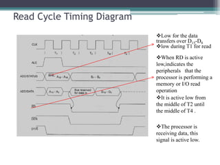
- 5. Read Cycle Timing Diagram Low for the data transfers over D15-D8 low during T1 for read When RD is active low,indicates the peripherals that the processor is performing a memory or I/O read operation The processor is receiving data, this signal is active low. It is active low from the middle of T2 until the middle of T4 .
- 6. Write Cycle Timing Diagram Processor sends out data, signal is active high.
- 7. Bus Request & Bus Grant Timings When the HOLD line goes high, it indicates to the processor that another master is requesting the bus access. After receiving the HOLD request, the processor issues the hold acknowledge signal on HLDA pin, in the middle of the next clock cycle after completing the current bus cycle.
- 8. Maximum Mode Configuration •The only difference lies in the status signals used and the available control and advanced command signals. •INTA pin used to issue two interrupt acknowledge pulses to the interrupt controller or to an interrupting device. •IORC, IOWC :These signals enable an IO interface to read or write the data from or to the address port. •The MRDC, MWTC : used as memory read or write signals. •All these command signals instructs the memory to accept or send data from or to the bus. •For both of these write command signals, the advanced signals namely AIOWC and AMWTC are available.
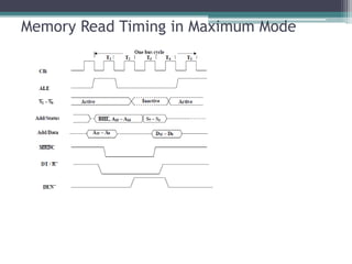
- 10. Memory Read Timing in Maximum Mode
- 11. Memory Write Timing in Maximum Mode
- 12. RQ/GT Timings in Maximum Mode. RQ/GT0,RQ/GT1 – Request/Grant: These pins are used by the other local bus master in maximum mode, to force the processor to release the local bus at the end of the processor current bus cycle.