Sequential logic circuit optimization
1 like881 views

The document discusses sequential logic circuits and finite state machines. It covers topics like combinational vs sequential logic, what defines a finite state machine, state transition diagrams, equivalent state partitioning for minimization, and applications like computer memory and delay elements. Examples are provided of a sequential circuit and its state table, as well as the process of state minimization.


![Digital systems principles and applications
oBy Tocci 2001
Synthesis And Optimization of Digital
circuits
o Giovani De Micheli
Digital Logic Design [Sequential circuits]
oDr. Eng. Ahmed H. Madian
http://en.wikipedia.org/wiki/Moore_machine
http://en.wikipedia.org/wiki/Mealy_machine
04/21/15 30](https://image.slidesharecdn.com/sequentiallogicoptimization-150421075320-conversion-gate01/85/Sequential-logic-circuit-optimization-30-320.jpg)

Sequential logic circuit optimization
- 1. 04/21/15 1 Ashis Kumar Chanda MS (2014-15), Roll 343 Department of Computer Science and Engineering University of Dhaka Submitted to: Prof. Hafiz Md. Hasan Babu
- 2. Logical Circuits Sequential Logical Circuits Finite State Machine Minimization Methods Applications Summary 04/21/15 2
- 3. If you have good CGPA score AND publications apply for research assistantship If you have good score OR presentation skill apply for teacher assistantship 04/21/15 3
- 4. 04/21/15 4 • We use a bit (binary digit), 0 or 1, to represent the state 0 (00) 1 (01) 2 (10) 3 (11)
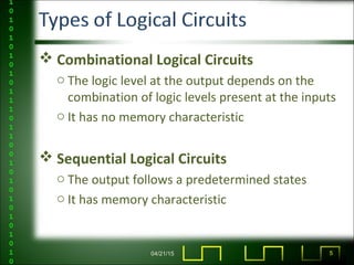
- 5. 04/21/15 5 Combinational Logical Circuits o The logic level at the output depends on the combination of logic levels present at the inputs o It has no memory characteristic Sequential Logical Circuits o The output follows a predetermined states o It has memory characteristic
- 6. 04/21/15 6 The word “Sequential” means that things happen in a “sequence” Why is it important? Need to follow synchronous process using clock signal
- 7. 04/21/15 7 Output is dependent on the input and the record of the input or state
- 8. 04/21/15 8 What is Finite State Diagrams? o The behavioral view of sequential circuits at logic level Why will we express a circuit in Finite State Diagrams? o state diagrams encapsulate the traces that the corresponding circuit can accept and produce
- 9. 04/21/15 9 oA set of primary input patterns, X oA set of primary output patterns, Y oA set of states, S oA state transition function oAn output transition function (Mealy model, Moore model)
- 10. For a Mealy machine, each arc (transition) is labeled with an output value. 04/21/15 10 The information in the state is typically written as q1q0 / Z q1q0 indicates the inputs, Z indicates output Ex: 01/1
- 11. A single input single output network that produces 1 if three consecutive 1's appear in the inputs. 04/21/15 11 S1 S2 S3 S4 1 1 1 0 0 0 0, 1
- 12. For a Moore machine, each node (state) is labeled with an output value; 04/21/15 12 Present state Next State for input 0, output Next state for input 1, output S1 S1 S0 S0 S0 S2 S2 S1 S0
- 13. 04/21/15 13 NOR D FF rr xx zz Input Current State Next State Output 0 S1 S2 1 0 S2 S1 0 1 S1 S1 0 1 S2 S1 0 r x Z 0 0 1 0 1 0 1 0 0 1 1 0 S1 S2 r/zr/z r/zr/z
- 14. 04/21/15 14 NOR D FF rr xx zz Input Current State Next State Output 0 S1 S2 1 0 S2 S1 0 1 S1 S1 0 1 S2 S1 0 r x Z 0 0 1 0 1 0 1 0 0 1 1 0 S1 S2 0/10/1
- 15. 04/21/15 15 NOR D FF rr xx zz r x Z 0 0 1 0 1 0 1 0 0 1 1 0 S1 S2 1/01/0 0/10/1 Input Current State Next State Output 0 S1 S2 1 0 S2 S1 0 1 S1 S1 0 1 S2 S1 0
- 16. 04/21/15 16 NOR D FF rr xx zz r x Z 0 0 1 0 1 0 1 0 0 1 1 0 S1 S2 1/01/0 0/10/1 0/00/0 Input Current State Next State Output 0 S1 S2 1 0 S2 S1 0 1 S1 S1 0 1 S2 S1 0
- 17. 04/21/15 17 NOR D FF rr xx zz r x Z 0 0 1 0 1 0 1 0 0 1 1 0 S1 S2 1/01/0 0/10/1 1/0 0/0 1/0 0/0 Input Current State Next State Output 0 S1 S2 1 0 S2 S1 0 1 S1 S1 0 1 S2 S1 0
- 18. 04/21/15 18 Completely specified Incompletely specified FSM FSM
- 19. 04/21/15 19
- 20. 04/21/15 20 Merge the equivalent states into a single state Two states are equivalent iff: oFor the same input, they have identical outputs oFor the same input, the corresponding next states are equivalent
- 21. 04/21/15 21 S3S1 S2 S4 S5 0/10/1 1/11/1 1/11/1 1/11/1 1/11/1 0/10/1 0/10/1 0/00/0 0/00/0 1/01/0
- 22. 04/21/15 22 Input Current State Next State Output 0 S1 S3 1 1 S1 S5 1 0 S2 S3 1 1 S2 S5 1 0 S3 S2 0 1 S3 S1 1 0 S4 S4 0 1 S4 S5 1 0 S5 S4 1 1 S5 S1 0 Output based partition -> {S1, S2} Next state based partition -> {{S1, S2}, {S3}, {S4}, {S5}} {S3, S4}, {S5}}
- 23. 04/21/15 23 Output based partition Next state based partition -> {{S1, S2}, {S3}, {S4}, {S5}} S1, S2 S3, S4 S5 P1 P2 P3
- 24. 04/21/15 24 Input Current State Next State Output 0 S12 S3 1 1 S12 S5 1 0 S3 S12 0 1 S3 S12 1 0 S4 S4 0 1 S4 S5 1 0 S5 S4 1 1 S5 S12 0
- 26. 04/21/15 26 The optimization process will reduce the area of circuit. So, we can save cost. It ensures better performance
- 27. 04/21/15 27 Computer memory Delay and storage elements Finite state machines Minimizing ensures smaller circuit area Better performance from fewer number of components
- 28. 04/21/15 28 Sequential logic circuit The minimization process Improvement in speed and cost Applications
- 30. Digital systems principles and applications oBy Tocci 2001 Synthesis And Optimization of Digital circuits o Giovani De Micheli Digital Logic Design [Sequential circuits] oDr. Eng. Ahmed H. Madian http://en.wikipedia.org/wiki/Moore_machine http://en.wikipedia.org/wiki/Mealy_machine 04/21/15 30
Editor's Notes
- #7: In general, human operator activates an input switch at random time. It is asynchronous process. This randomness can produce unpredictable and undesirable results. Thus, we need to follow synchronous process using clock signal