SlideShare a Scribd company logo
UNIT 5 – Assembly
Language Programming
-By
Prof. K. U. Sharma
8086 Input/output & 8255 PPI
Contents:
1. Mapping Schemes
 Memory Mapped I/O
 I/O Mapped I/O
2. Bus Cycle & Time States
 Minimum Mode and Maximum Mode Bus Cycles
3. Intel 8255 PPI
 I/O Mode
 BSR Mode
4. Programming with 8255
4/1/2014
Prof. K. U. Sharma, PRMCEAM, Contact:
karthik8777@gmail.com, 9096996329
8086’s I/O:
 An i/o addressing capacity of 8086 is of 16-bit, so total i/o’s that can be
addressed by the microprocessor are 216 = 64kb.
 In I/O addressing there is no role of segment registers.
 An I/O can be mapped in two ways
1. Memory Mapped I/O
2. I/O Mapped I/O
4/1/2014
Prof. K. U. Sharma, PRMCEAM, Contact:
karthik8777@gmail.com, 9096996329
1. Memory Mapped I/O:
 Whenever the addresses of I/O’s are inserted in the span of memory, then
the scheme is called memory mapped I/O.
Advantage: There is no need of separate hardware & software to implement
this scheme.
Disadvantage: Due to insertion of I/O’s, memory space is reduced.
Memory I/O
1 MB
4/1/2014
Prof. K. U. Sharma, PRMCEAM, Contact:
karthik8777@gmail.com, 9096996329
2. Memory Mapped I/O:
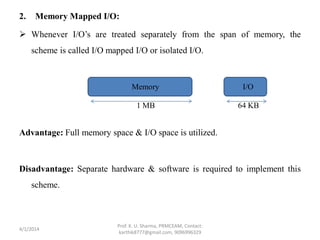
 Whenever I/O’s are treated separately from the span of memory, the
scheme is called I/O mapped I/O or isolated I/O.
Advantage: Full memory space & I/O space is utilized.
Disadvantage: Separate hardware & software is required to implement this
scheme.
Memory
1 MB
I/O
64 KB
4/1/2014
Prof. K. U. Sharma, PRMCEAM, Contact:
karthik8777@gmail.com, 9096996329
Inst Related to the Above Schemes:
 Intel 8086 provides the following two inst for implementing his schemes:
1. IN
2. OUT
1. IN:
1. IN PORTADD (8);
Example:
IN AL, 09;  (09)  (AL)
 In the above inst, the 8 bit content of PORTADD is copied to AL register.
Here the address of port is directly given hence this inst involves direct
addressing mode.
4/1/2014
Prof. K. U. Sharma, PRMCEAM, Contact:
karthik8777@gmail.com, 9096996329
2. IN AX, PORTADD (8);
Example:
IN AX, 09;
 (09)  (AL) and
(0A)  (AH)
This inst follows direct addressing mode.
3. IN AL, [DX];
 ((DX))  (AL)
 In the above inst, the address of 16 bit is indirectly specified through DX
register; the 8 bit contents of that port address will be copied to the AL
register. This inst involves register indirect addressing mode.
4/1/2014
Prof. K. U. Sharma, PRMCEAM, Contact:
karthik8777@gmail.com, 9096996329
4. IN AX, [DX];
 ((DX))  (AL)
((DX+1))  (AH)
Register Indirect Addressing mode.
2. OUT:
1. OUT PORTADD AL;
Example:
OUT 09, AL;  (AL)  (09)
4/1/2014
Prof. K. U. Sharma, PRMCEAM, Contact:
karthik8777@gmail.com, 9096996329
2. OUT PORTADD, AX;
Example:
OUT CD, AX;  (AL)  (CD) and
(AH)  (CE)
In the above inst the content of AL register is copied to the content of port
whose address is directly mentioned inside the inst whereas the content of
AH register is copied to (port add + 1).
3. OUT [DX], AL;
 (AL)  ((DX))
4. OUT [DX], AX;
 (AL)  ((DX))
(AH)  ((DX)+1)
4/1/2014
Prof. K. U. Sharma, PRMCEAM, Contact:
karthik8777@gmail.com, 9096996329
Intel 8255 (Programmable Peripheral Interface)
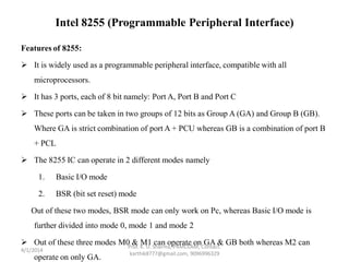
Features of 8255:
 It is widely used as a programmable peripheral interface, compatible with all
microprocessors.
 It has 3 ports, each of 8 bit namely: Port A, Port B and Port C
 These ports can be taken in two groups of 12 bits as Group A (GA) and Group B (GB).
Where GA is strict combination of port A + PCU whereas GB is a combination of port B
+ PCL
 The 8255 IC can operate in 2 different modes namely
1. Basic I/O mode
2. BSR (bit set reset) mode
Out of these two modes, BSR mode can only work on Pc, whereas Basic I/O mode is
further divided into mode 0, mode 1 and mode 2
 Out of these three modes M0 & M1 can operate on GA & GB both whereas M2 can
operate on only GA.
4/1/2014
Prof. K. U. Sharma, PRMCEAM, Contact:
karthik8777@gmail.com, 9096996329
4/1/2014
Prof. K. U. Sharma, PRMCEAM, Contact:
karthik8777@gmail.com, 9096996329
Control Register Types:
 There are 2 types of control registers; one for basic i/o mode and one for BSR
mode.
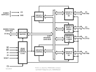
 Depending upon the address lines A0 & A1, the selection of different ports is made
as follows:
 Data bus buffer is of 8 bits, which is used to interface with microprocessor for
handling 8 bit data.
 The read/write is responsible for read write operations.
 The CS signal is generated by the microprocessor using address decoding logic.
A1 A0 Selection
0 0 PA
0 1 PB
1 0 PC
1 1 CWR
4/1/2014
Prof. K. U. Sharma, PRMCEAM, Contact:
karthik8777@gmail.com, 9096996329
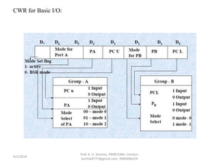
CWR for Basic I/O:
4/1/2014
Prof. K. U. Sharma, PRMCEAM, Contact:
karthik8777@gmail.com, 9096996329
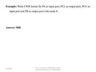
Example: Write CWR format for PA as input port, PCL as output port, PCU as
input port and PB as output port with mode 0 .
Answer: 98H
4/1/2014
Prof. K. U. Sharma, PRMCEAM, Contact:
karthik8777@gmail.com, 9096996329
4/1/2014
Prof. K. U. Sharma, PRMCEAM, Contact:
karthik8777@gmail.com, 9096996329
CWR for BSR Mode:
 The range defined for BSR is from 0 to 7F and for basic I/O is from 80H to
FF.
Example: Write a BSR CWR value to set PC3 & PC6 of 8255
Answer:
1. 07H
2. 0DH
4/1/2014
Prof. K. U. Sharma, PRMCEAM, Contact:
karthik8777@gmail.com, 9096996329
Modes of Basic I/O:
 There are 3 basic types of different i/o modes listed as
1. Mode 0
2. Mode 1
3. Mode 2
MODE 0: (Simple i/o or Basic i/o without Handshaking)
 In this mode, any of the port can be used as input or output port depending upon the
bit setting in control register. Also called as default mode.
 In this mode, there are no handshakes signals, handshakes signals are those which
are used to check the device status before making the actual data transfer.
4/1/2014
Prof. K. U. Sharma, PRMCEAM, Contact:
karthik8777@gmail.com, 9096996329
MODE 1: (Strobed i/o with Handshakes)
 This mode is also called as strobed i/o with unidirectional handshakes, both GA and
GB can operate in this mode either together or individually.
 Here each group will use 8 bit for actual data transfer whereas bits of PC are used
for handshake signals.
Case 1: When PA & PB are acting as I/P ports
4/1/2014
Prof. K. U. Sharma, PRMCEAM, Contact:
karthik8777@gmail.com, 9096996329
 When PA & PB are operating as input ports, there are various handshake
signals described:
1. STB: The strobe input signal is given by standard input devices, which
when goes low indicates that the data is ready with source device & it is
ready to strobe or load in to respective port.
2. IBF (Input Buffer Full): Once the data is available inside port, this signal
goes high indicating input buffer full.
3. INTR: This is an output signal which is used to interrupt the
microprocessor for requesting it to read the data. Once data is read by the
microprocessor then the IBF signal goes low.
4/1/2014
Prof. K. U. Sharma, PRMCEAM, Contact:
karthik8777@gmail.com, 9096996329
Case 2: When PA & PB are acting as O/P ports
4/1/2014
Prof. K. U. Sharma, PRMCEAM, Contact:
karthik8777@gmail.com, 9096996329
• When PA & PB is acting as output port then following handshakes signals
are used:
1. INTR: It is an interrupt request made to the microprocessor demanding
for data from microprocessor.
2. OBF: This is an active low output buffer full signal which indicates that
respective port available with the 8-bit data in it.
3. ACK: This is an active low acknowledgment input signal given by the
destination device making sure that the data which is transferred by 8255
is being received by destination.
4/1/2014
Prof. K. U. Sharma, PRMCEAM, Contact:
karthik8777@gmail.com, 9096996329
MODE 2: (Bidirectional strobed I/O with handshake)
4/1/2014
Prof. K. U. Sharma, PRMCEAM, Contact:
karthik8777@gmail.com, 9096996329
• This mode is called as bidirectional strobed I/O with handshake. It is
applicable on GA only.
• In the above figure OBF & ACK are used for output operation & STB and
IBF will be used for input operation.
Problem:
1. Write a program for reading the data from PA & PB. AND this data & put
the ANDING result in PC.
4/1/2014
Prof. K. U. Sharma, PRMCEAM, Contact:
karthik8777@gmail.com, 9096996329
Answer:
Assuming an address of CWR as F6H, hence the addresses of different
ports will F4H, F2H and F0H for port C , B, A respectively.
Defining the CWR = 92H
Mov AL, 92H
OUT F6, AL ; Initializing the CWR
IN AL, F0H ; Reading data from PA
Mov BL, AL
IN AL, F2H ; Reading data from PB
AND AL, BL ;
OUT F4, AL ; Writing the result to PC
HLT
4/1/2014
Prof. K. U. Sharma, PRMCEAM, Contact:
karthik8777@gmail.com, 9096996329
Program:
1. PPI is configured so that PA is an output port, both ports B and C are input ports, and
all three ports are set up for mode 0 operation. Write a program that will input the data
at ports B and C, find the difference (port C) – (port B), and output this difference to
port A.
2. Data are to be read in from two byte wide input ports at addresses AA and A9 and then
output as a word to a word wide output port at address B000. Write a sequence of inst
to perform this i/o operations.
3. What control word must be written into the control register of the 8255 such that port A
is configured for bidirectional operation and port B is set up with mode 1 outputs.
4. Write a sequence of inst that will input the contents of the input port at i/o address B0H
and jump to the beginning of a service routine identified by the label ACTIVE INPUT
if the LSB of the data is 1.
4/1/2014
Prof. K. U. Sharma, PRMCEAM, Contact:
karthik8777@gmail.com, 9096996329
Answers:
1. Assuming the addresses of the ports as
Port A = 30H; Port B = 32H; Port C = 34H
IN AL, 32H ; Reading port B
Mov BL, AL ; Saving the data
IN AL, 34H ; Reading port C
SUB AL, BL ; subtract B from C
OUT 30H, AL ; write to port A
4/1/2014
Prof. K. U. Sharma, PRMCEAM, Contact:
karthik8777@gmail.com, 9096996329
Answers:
2. IN AL, 0AAH ;
Mov AH, AL ;
IN AL, 0A9H ;
Mov DX, 0B000H
OUT DX, AX
HLT
3. CWR = C4H
4/1/2014
Prof. K. U. Sharma, PRMCEAM, Contact:
karthik8777@gmail.com, 9096996329
Answers:
4. Mov DX, 00B0H ; set port address
IN AL, DX ; receive data
TEST AL, 1 ; test LSB port
JNZ NEXT ; jump to next inst if LSB is 0
JMPACTIVE INPUT ; jump to this routine when LSB is 1.
4/1/2014
Prof. K. U. Sharma, PRMCEAM, Contact:
karthik8777@gmail.com, 9096996329
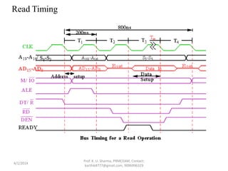
Bus Timing
• The 8086/8088 microprocessors use the memory and I/O in periods called
bus cycles.
• Each bus cycle consists of 4 clock cycles.
• Thus for 8086 running at 5MHz it would take 800ns for a complete bus
cycle.
• Each read or write operation takes 1 bus cycles.
4/1/2014
Prof. K. U. Sharma, PRMCEAM, Contact:
karthik8777@gmail.com, 9096996329
Read Timing
4/1/2014
Prof. K. U. Sharma, PRMCEAM, Contact:
karthik8777@gmail.com, 9096996329
31
During T 1 :
The address is placed on the Address/Data
bus.
Control signals M/ IO , ALE and DT/ R
specify memory or I/O, latch the address
onto the address bus and set the direction of
data transfer on data bus.
32
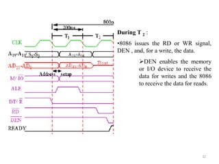
During T 2 :
•8086 issues the RD or WR signal,
DEN , and, for a write, the data.
DEN enables the memory
or I/O device to receive the
data for writes and the 8086
to receive the data for reads.
33
During T 3 :
•This cycle is provided to allow memory to access data.
•READY is sampled at the end of T 2 .
If low, T 3 becomes a wait state.
Otherwise, the data bus is sampled at the end of T 3 .
34
During T 4 :
All bus signals are deactivated, in preparation for next bus cycle.
Data is sampled for reads, writes occur for writes.
35
Write Timing

More Related Content

What's hot (20)

PPTX
Leakage effects in mos-fets
Arya Ls
 
PDF
8255 programable io
prabhat pandey
 
DOC
Qoestion Bank Big Questions
ccet
 
PDF
8051 (microcontroller)class1
Nitin Ahire
 
PDF
Lab 7 -RAM and ROM, Xilinx, Digelent BASYS experimentor board
Katrina Little
 
PPTX
Rc delay modelling in vlsi
Dr. Vishal Sharma
 
PPT
8251 communication interface
LingalaSowjanya
 
PDF
8051 microcontroller
Gaurav Verma
 
PPTX
Microcontroller 8051
Patruni Chidananda Sastry
 
PPTX
Programmable logic array (pla)
Zainab Noor
 
PPT
Microcontroller 8051
Rashmi
 
PDF
CMOS Topic 5 -_cmos_inverter
Ikhwan_Fakrudin
 
PPTX
Demultiplexer presentation
Shaikat Saha
 
PDF
Layout02 (1)
venkat1234_nxp
 
PDF
RF Circuit Design - [Ch3-2] Power Waves and Power-Gain Expressions
Simen Li
 
PDF
Counters
Ravi Maurya
 
DOCX
UNIT-IV .FINITE STATE MACHINES
Dr.YNM
 
PDF
Multiband Transceivers - [Chapter 2] Noises and Linearities
Simen Li
 
PDF
IC Design of Power Management Circuits (II)
Claudia Sin
 
PPTX
8085 MICROPROCESSOR ARCHITECTURE AND ITS OPERATIONS
RamaPrabha24
 
Leakage effects in mos-fets
Arya Ls
 
8255 programable io
prabhat pandey
 
Qoestion Bank Big Questions
ccet
 
8051 (microcontroller)class1
Nitin Ahire
 
Lab 7 -RAM and ROM, Xilinx, Digelent BASYS experimentor board
Katrina Little
 
Rc delay modelling in vlsi
Dr. Vishal Sharma
 
8251 communication interface
LingalaSowjanya
 
8051 microcontroller
Gaurav Verma
 
Microcontroller 8051
Patruni Chidananda Sastry
 
Programmable logic array (pla)
Zainab Noor
 
Microcontroller 8051
Rashmi
 
CMOS Topic 5 -_cmos_inverter
Ikhwan_Fakrudin
 
Demultiplexer presentation
Shaikat Saha
 
Layout02 (1)
venkat1234_nxp
 
RF Circuit Design - [Ch3-2] Power Waves and Power-Gain Expressions
Simen Li
 
Counters
Ravi Maurya
 
UNIT-IV .FINITE STATE MACHINES
Dr.YNM
 
Multiband Transceivers - [Chapter 2] Noises and Linearities
Simen Li
 
IC Design of Power Management Circuits (II)
Claudia Sin
 
8085 MICROPROCESSOR ARCHITECTURE AND ITS OPERATIONS
RamaPrabha24
 

Viewers also liked (19)

PDF
microprocessor & programming
Gaurang Thakar
 
PPT
1204 Ppi 8255
techbed
 
PPT
Interfacing 8255
Anuja Bhakuni
 
PDF
Beginner avr
Getachew Mamo
 
PPTX
Lesson 04
Tracie King
 
PDF
Pic assembly launguage
kishore_435
 
PPT
Display1in mp
Aisu
 
PDF
Coal 5 memory reading concepts in Assembly Programming
Muhammad Taqi Hassan Bukhari
 
PPTX
8255:ppi & 8259:pic
Adarsh Patel
 
PPTX
8255 PPI
deval patel
 
PPT
1203 Ppi 8155
techbed
 
PPT
8255_utkarsh_kulshrestha
Utkarsh Kulshrestha
 
PPTX
Direct memory access (dma) with 8257 DMA Controller
Muhammed Afsal Villan
 
PPSX
8051 architecture
sb108ec
 
PPTX
Direct Memory Access(DMA)
Page Maker
 
PDF
Question paper with solution the 8051 microcontroller based embedded systems...
manishpatel_79
 
PPTX
Chapter 5 - Fuzzy Logic
Ashique Rasool
 
PDF
Embedded C programming based on 8051 microcontroller
Gaurav Verma
 
PDF
The Top Skills That Can Get You Hired in 2017
LinkedIn
 
microprocessor & programming
Gaurang Thakar
 
1204 Ppi 8255
techbed
 
Interfacing 8255
Anuja Bhakuni
 
Beginner avr
Getachew Mamo
 
Lesson 04
Tracie King
 
Pic assembly launguage
kishore_435
 
Display1in mp
Aisu
 
Coal 5 memory reading concepts in Assembly Programming
Muhammad Taqi Hassan Bukhari
 
8255:ppi & 8259:pic
Adarsh Patel
 
8255 PPI
deval patel
 
1203 Ppi 8155
techbed
 
8255_utkarsh_kulshrestha
Utkarsh Kulshrestha
 
Direct memory access (dma) with 8257 DMA Controller
Muhammed Afsal Villan
 
8051 architecture
sb108ec
 
Direct Memory Access(DMA)
Page Maker
 
Question paper with solution the 8051 microcontroller based embedded systems...
manishpatel_79
 
Chapter 5 - Fuzzy Logic
Ashique Rasool
 
Embedded C programming based on 8051 microcontroller
Gaurav Verma
 
The Top Skills That Can Get You Hired in 2017
LinkedIn
 
Ad

Similar to Unit 5 assembly language programming (20)

PPTX
8255 Programmble Peripheral Interface
Amit Kumer Podder
 
PPT
8255 presentaion.ppt
kamlesh deshmukh
 
PDF
8255 & IO Interfacing.pdf
Ilavarasan Tamizh
 
PPTX
Unit-3 IO Interfacing-1.pptximportant questions to be noted
mandakalyan811
 
PPT
8255 class
riyasekaran
 
PPTX
L4-L6 8255 A.pptx
Motaleb Hossen Manik
 
PPT
Ppi 8255
Muhammadalizardari
 
PDF
Unit 3-PROGRAMMABLE PERIPERAL INTERFACE.pdf- MECHATRONICS-ENGGINERING
Chandra Kumar S
 
PPTX
Operation of 8255A
Anuj Yadav
 
PDF
unit-3-8255.pdf
ShanmukhSaiR
 
PPTX
8255 ppi.pptx
zahid235639
 
PPTX
8255 ppi students material for ppi mpmc study
Sirisha Vamsi
 
PPTX
UNIT- 3.pptx
BASKARS53
 
PPTX
25. 8255 programmable peripheral interface
sandip das
 
PPTX
8086 microprocessor -Input/Output INTERFACING
C.Helen Sulochana
 
PPTX
UNIT 3 Peripheral Interfacing.pptx
Gowrishankar C
 
PPT
MECHATRONICS-Unit 3-PROGRAMMABLE PERIPERAL INTERFACE.ppt
CHANDRA KUMAR S
 
PPT
8255 PPI (programmable Peripheral Interface) mode 0
ABHIMANYUJHA8
 
PPT
Programmableperipheralinterface 8255 ppt
sharan Kumar
 
PPTX
Lec14
siddu kadiwal
 
8255 Programmble Peripheral Interface
Amit Kumer Podder
 
8255 presentaion.ppt
kamlesh deshmukh
 
8255 & IO Interfacing.pdf
Ilavarasan Tamizh
 
Unit-3 IO Interfacing-1.pptximportant questions to be noted
mandakalyan811
 
8255 class
riyasekaran
 
L4-L6 8255 A.pptx
Motaleb Hossen Manik
 
Unit 3-PROGRAMMABLE PERIPERAL INTERFACE.pdf- MECHATRONICS-ENGGINERING
Chandra Kumar S
 
Operation of 8255A
Anuj Yadav
 
unit-3-8255.pdf
ShanmukhSaiR
 
8255 ppi.pptx
zahid235639
 
8255 ppi students material for ppi mpmc study
Sirisha Vamsi
 
UNIT- 3.pptx
BASKARS53
 
25. 8255 programmable peripheral interface
sandip das
 
8086 microprocessor -Input/Output INTERFACING
C.Helen Sulochana
 
UNIT 3 Peripheral Interfacing.pptx
Gowrishankar C
 
MECHATRONICS-Unit 3-PROGRAMMABLE PERIPERAL INTERFACE.ppt
CHANDRA KUMAR S
 
8255 PPI (programmable Peripheral Interface) mode 0
ABHIMANYUJHA8
 
Programmableperipheralinterface 8255 ppt
sharan Kumar
 
Ad

Recently uploaded (20)

PPTX
MODULE 03 - CLOUD COMPUTING AND SECURITY.pptx
Alvas Institute of Engineering and technology, Moodabidri
 
PPTX
Distribution reservoir and service storage pptx
dhanashree78
 
PPTX
DATA BASE MANAGEMENT AND RELATIONAL DATA
gomathisankariv2
 
PPT
Testing and final inspection of a solar PV system
MuhammadSanni2
 
PDF
Pressure Measurement training for engineers and Technicians
AIESOLUTIONS
 
PDF
MODULE-5 notes [BCG402-CG&V] PART-B.pdf
Alvas Institute of Engineering and technology, Moodabidri
 
PDF
20ES1152 Programming for Problem Solving Lab Manual VRSEC.pdf
Ashutosh Satapathy
 
PPTX
Water Resources Engineering (CVE 728)--Slide 3.pptx
mohammedado3
 
PDF
Viol_Alessandro_Presentazione_prelaurea.pdf
dsecqyvhbowrzxshhf
 
PPTX
How Industrial Project Management Differs From Construction.pptx
jamespit799
 
PDF
methodology-driven-mbse-murphy-july-hsv-huntsville6680038572db67488e78ff00003...
henriqueltorres1
 
PDF
SERVERLESS PERSONAL TO-DO LIST APPLICATION
anushaashraf20
 
PPTX
Final Major project a b c d e f g h i j k l m
bharathpsnab
 
PDF
Electrical Machines and Their Protection.pdf
Nabajyoti Banik
 
PPTX
GitOps_Without_K8s_Training_detailed git repository
DanialHabibi2
 
PPTX
MODULE 05 - CLOUD COMPUTING AND SECURITY.pptx
Alvas Institute of Engineering and technology, Moodabidri
 
PDF
REINFORCEMENT LEARNING IN DECISION MAKING SEMINAR REPORT
anushaashraf20
 
PPTX
Water Resources Engineering (CVE 728)--Slide 4.pptx
mohammedado3
 
PDF
Electrical Engineer operation Supervisor
ssaruntatapower143
 
PPTX
Introduction to Internal Combustion Engines - Types, Working and Camparison.pptx
UtkarshPatil98
 
MODULE 03 - CLOUD COMPUTING AND SECURITY.pptx
Alvas Institute of Engineering and technology, Moodabidri
 
Distribution reservoir and service storage pptx
dhanashree78
 
DATA BASE MANAGEMENT AND RELATIONAL DATA
gomathisankariv2
 
Testing and final inspection of a solar PV system
MuhammadSanni2
 
Pressure Measurement training for engineers and Technicians
AIESOLUTIONS
 
MODULE-5 notes [BCG402-CG&V] PART-B.pdf
Alvas Institute of Engineering and technology, Moodabidri
 
20ES1152 Programming for Problem Solving Lab Manual VRSEC.pdf
Ashutosh Satapathy
 
Water Resources Engineering (CVE 728)--Slide 3.pptx
mohammedado3
 
Viol_Alessandro_Presentazione_prelaurea.pdf
dsecqyvhbowrzxshhf
 
How Industrial Project Management Differs From Construction.pptx
jamespit799
 
methodology-driven-mbse-murphy-july-hsv-huntsville6680038572db67488e78ff00003...
henriqueltorres1
 
SERVERLESS PERSONAL TO-DO LIST APPLICATION
anushaashraf20
 
Final Major project a b c d e f g h i j k l m
bharathpsnab
 
Electrical Machines and Their Protection.pdf
Nabajyoti Banik
 
GitOps_Without_K8s_Training_detailed git repository
DanialHabibi2
 
MODULE 05 - CLOUD COMPUTING AND SECURITY.pptx
Alvas Institute of Engineering and technology, Moodabidri
 
REINFORCEMENT LEARNING IN DECISION MAKING SEMINAR REPORT
anushaashraf20
 
Water Resources Engineering (CVE 728)--Slide 4.pptx
mohammedado3
 
Electrical Engineer operation Supervisor
ssaruntatapower143
 
Introduction to Internal Combustion Engines - Types, Working and Camparison.pptx
UtkarshPatil98
 

Unit 5 assembly language programming

  • 1. UNIT 5 – Assembly Language Programming -By Prof. K. U. Sharma
  • 2. 8086 Input/output & 8255 PPI Contents: 1. Mapping Schemes  Memory Mapped I/O  I/O Mapped I/O 2. Bus Cycle & Time States  Minimum Mode and Maximum Mode Bus Cycles 3. Intel 8255 PPI  I/O Mode  BSR Mode 4. Programming with 8255 4/1/2014 Prof. K. U. Sharma, PRMCEAM, Contact: [email protected], 9096996329
  • 3. 8086’s I/O:  An i/o addressing capacity of 8086 is of 16-bit, so total i/o’s that can be addressed by the microprocessor are 216 = 64kb.  In I/O addressing there is no role of segment registers.  An I/O can be mapped in two ways 1. Memory Mapped I/O 2. I/O Mapped I/O 4/1/2014 Prof. K. U. Sharma, PRMCEAM, Contact: [email protected], 9096996329
  • 4. 1. Memory Mapped I/O:  Whenever the addresses of I/O’s are inserted in the span of memory, then the scheme is called memory mapped I/O. Advantage: There is no need of separate hardware & software to implement this scheme. Disadvantage: Due to insertion of I/O’s, memory space is reduced. Memory I/O 1 MB 4/1/2014 Prof. K. U. Sharma, PRMCEAM, Contact: [email protected], 9096996329
  • 5. 2. Memory Mapped I/O:  Whenever I/O’s are treated separately from the span of memory, the scheme is called I/O mapped I/O or isolated I/O. Advantage: Full memory space & I/O space is utilized. Disadvantage: Separate hardware & software is required to implement this scheme. Memory 1 MB I/O 64 KB 4/1/2014 Prof. K. U. Sharma, PRMCEAM, Contact: [email protected], 9096996329
  • 6. Inst Related to the Above Schemes:  Intel 8086 provides the following two inst for implementing his schemes: 1. IN 2. OUT 1. IN: 1. IN PORTADD (8); Example: IN AL, 09;  (09)  (AL)  In the above inst, the 8 bit content of PORTADD is copied to AL register. Here the address of port is directly given hence this inst involves direct addressing mode. 4/1/2014 Prof. K. U. Sharma, PRMCEAM, Contact: [email protected], 9096996329
  • 7. 2. IN AX, PORTADD (8); Example: IN AX, 09;  (09)  (AL) and (0A)  (AH) This inst follows direct addressing mode. 3. IN AL, [DX];  ((DX))  (AL)  In the above inst, the address of 16 bit is indirectly specified through DX register; the 8 bit contents of that port address will be copied to the AL register. This inst involves register indirect addressing mode. 4/1/2014 Prof. K. U. Sharma, PRMCEAM, Contact: [email protected], 9096996329
  • 8. 4. IN AX, [DX];  ((DX))  (AL) ((DX+1))  (AH) Register Indirect Addressing mode. 2. OUT: 1. OUT PORTADD AL; Example: OUT 09, AL;  (AL)  (09) 4/1/2014 Prof. K. U. Sharma, PRMCEAM, Contact: [email protected], 9096996329
  • 9. 2. OUT PORTADD, AX; Example: OUT CD, AX;  (AL)  (CD) and (AH)  (CE) In the above inst the content of AL register is copied to the content of port whose address is directly mentioned inside the inst whereas the content of AH register is copied to (port add + 1). 3. OUT [DX], AL;  (AL)  ((DX)) 4. OUT [DX], AX;  (AL)  ((DX)) (AH)  ((DX)+1) 4/1/2014 Prof. K. U. Sharma, PRMCEAM, Contact: [email protected], 9096996329
  • 10. Intel 8255 (Programmable Peripheral Interface) Features of 8255:  It is widely used as a programmable peripheral interface, compatible with all microprocessors.  It has 3 ports, each of 8 bit namely: Port A, Port B and Port C  These ports can be taken in two groups of 12 bits as Group A (GA) and Group B (GB). Where GA is strict combination of port A + PCU whereas GB is a combination of port B + PCL  The 8255 IC can operate in 2 different modes namely 1. Basic I/O mode 2. BSR (bit set reset) mode Out of these two modes, BSR mode can only work on Pc, whereas Basic I/O mode is further divided into mode 0, mode 1 and mode 2  Out of these three modes M0 & M1 can operate on GA & GB both whereas M2 can operate on only GA. 4/1/2014 Prof. K. U. Sharma, PRMCEAM, Contact: [email protected], 9096996329
  • 11. 4/1/2014 Prof. K. U. Sharma, PRMCEAM, Contact: [email protected], 9096996329
  • 12. Control Register Types:  There are 2 types of control registers; one for basic i/o mode and one for BSR mode.  Depending upon the address lines A0 & A1, the selection of different ports is made as follows:  Data bus buffer is of 8 bits, which is used to interface with microprocessor for handling 8 bit data.  The read/write is responsible for read write operations.  The CS signal is generated by the microprocessor using address decoding logic. A1 A0 Selection 0 0 PA 0 1 PB 1 0 PC 1 1 CWR 4/1/2014 Prof. K. U. Sharma, PRMCEAM, Contact: [email protected], 9096996329
  • 13. CWR for Basic I/O: 4/1/2014 Prof. K. U. Sharma, PRMCEAM, Contact: [email protected], 9096996329
  • 14. Example: Write CWR format for PA as input port, PCL as output port, PCU as input port and PB as output port with mode 0 . Answer: 98H 4/1/2014 Prof. K. U. Sharma, PRMCEAM, Contact: [email protected], 9096996329
  • 15. 4/1/2014 Prof. K. U. Sharma, PRMCEAM, Contact: [email protected], 9096996329 CWR for BSR Mode:
  • 16.  The range defined for BSR is from 0 to 7F and for basic I/O is from 80H to FF. Example: Write a BSR CWR value to set PC3 & PC6 of 8255 Answer: 1. 07H 2. 0DH 4/1/2014 Prof. K. U. Sharma, PRMCEAM, Contact: [email protected], 9096996329
  • 17. Modes of Basic I/O:  There are 3 basic types of different i/o modes listed as 1. Mode 0 2. Mode 1 3. Mode 2 MODE 0: (Simple i/o or Basic i/o without Handshaking)  In this mode, any of the port can be used as input or output port depending upon the bit setting in control register. Also called as default mode.  In this mode, there are no handshakes signals, handshakes signals are those which are used to check the device status before making the actual data transfer. 4/1/2014 Prof. K. U. Sharma, PRMCEAM, Contact: [email protected], 9096996329
  • 18. MODE 1: (Strobed i/o with Handshakes)  This mode is also called as strobed i/o with unidirectional handshakes, both GA and GB can operate in this mode either together or individually.  Here each group will use 8 bit for actual data transfer whereas bits of PC are used for handshake signals. Case 1: When PA & PB are acting as I/P ports 4/1/2014 Prof. K. U. Sharma, PRMCEAM, Contact: [email protected], 9096996329
  • 19.  When PA & PB are operating as input ports, there are various handshake signals described: 1. STB: The strobe input signal is given by standard input devices, which when goes low indicates that the data is ready with source device & it is ready to strobe or load in to respective port. 2. IBF (Input Buffer Full): Once the data is available inside port, this signal goes high indicating input buffer full. 3. INTR: This is an output signal which is used to interrupt the microprocessor for requesting it to read the data. Once data is read by the microprocessor then the IBF signal goes low. 4/1/2014 Prof. K. U. Sharma, PRMCEAM, Contact: [email protected], 9096996329
  • 20. Case 2: When PA & PB are acting as O/P ports 4/1/2014 Prof. K. U. Sharma, PRMCEAM, Contact: [email protected], 9096996329
  • 21. • When PA & PB is acting as output port then following handshakes signals are used: 1. INTR: It is an interrupt request made to the microprocessor demanding for data from microprocessor. 2. OBF: This is an active low output buffer full signal which indicates that respective port available with the 8-bit data in it. 3. ACK: This is an active low acknowledgment input signal given by the destination device making sure that the data which is transferred by 8255 is being received by destination. 4/1/2014 Prof. K. U. Sharma, PRMCEAM, Contact: [email protected], 9096996329
  • 22. MODE 2: (Bidirectional strobed I/O with handshake) 4/1/2014 Prof. K. U. Sharma, PRMCEAM, Contact: [email protected], 9096996329
  • 23. • This mode is called as bidirectional strobed I/O with handshake. It is applicable on GA only. • In the above figure OBF & ACK are used for output operation & STB and IBF will be used for input operation. Problem: 1. Write a program for reading the data from PA & PB. AND this data & put the ANDING result in PC. 4/1/2014 Prof. K. U. Sharma, PRMCEAM, Contact: [email protected], 9096996329
  • 24. Answer: Assuming an address of CWR as F6H, hence the addresses of different ports will F4H, F2H and F0H for port C , B, A respectively. Defining the CWR = 92H Mov AL, 92H OUT F6, AL ; Initializing the CWR IN AL, F0H ; Reading data from PA Mov BL, AL IN AL, F2H ; Reading data from PB AND AL, BL ; OUT F4, AL ; Writing the result to PC HLT 4/1/2014 Prof. K. U. Sharma, PRMCEAM, Contact: [email protected], 9096996329
  • 25. Program: 1. PPI is configured so that PA is an output port, both ports B and C are input ports, and all three ports are set up for mode 0 operation. Write a program that will input the data at ports B and C, find the difference (port C) – (port B), and output this difference to port A. 2. Data are to be read in from two byte wide input ports at addresses AA and A9 and then output as a word to a word wide output port at address B000. Write a sequence of inst to perform this i/o operations. 3. What control word must be written into the control register of the 8255 such that port A is configured for bidirectional operation and port B is set up with mode 1 outputs. 4. Write a sequence of inst that will input the contents of the input port at i/o address B0H and jump to the beginning of a service routine identified by the label ACTIVE INPUT if the LSB of the data is 1. 4/1/2014 Prof. K. U. Sharma, PRMCEAM, Contact: [email protected], 9096996329
  • 26. Answers: 1. Assuming the addresses of the ports as Port A = 30H; Port B = 32H; Port C = 34H IN AL, 32H ; Reading port B Mov BL, AL ; Saving the data IN AL, 34H ; Reading port C SUB AL, BL ; subtract B from C OUT 30H, AL ; write to port A 4/1/2014 Prof. K. U. Sharma, PRMCEAM, Contact: [email protected], 9096996329
  • 27. Answers: 2. IN AL, 0AAH ; Mov AH, AL ; IN AL, 0A9H ; Mov DX, 0B000H OUT DX, AX HLT 3. CWR = C4H 4/1/2014 Prof. K. U. Sharma, PRMCEAM, Contact: [email protected], 9096996329
  • 28. Answers: 4. Mov DX, 00B0H ; set port address IN AL, DX ; receive data TEST AL, 1 ; test LSB port JNZ NEXT ; jump to next inst if LSB is 0 JMPACTIVE INPUT ; jump to this routine when LSB is 1. 4/1/2014 Prof. K. U. Sharma, PRMCEAM, Contact: [email protected], 9096996329
  • 29. Bus Timing • The 8086/8088 microprocessors use the memory and I/O in periods called bus cycles. • Each bus cycle consists of 4 clock cycles. • Thus for 8086 running at 5MHz it would take 800ns for a complete bus cycle. • Each read or write operation takes 1 bus cycles. 4/1/2014 Prof. K. U. Sharma, PRMCEAM, Contact: [email protected], 9096996329
  • 30. Read Timing 4/1/2014 Prof. K. U. Sharma, PRMCEAM, Contact: [email protected], 9096996329
  • 31. 31 During T 1 : The address is placed on the Address/Data bus. Control signals M/ IO , ALE and DT/ R specify memory or I/O, latch the address onto the address bus and set the direction of data transfer on data bus.
  • 32. 32 During T 2 : •8086 issues the RD or WR signal, DEN , and, for a write, the data. DEN enables the memory or I/O device to receive the data for writes and the 8086 to receive the data for reads.
  • 33. 33 During T 3 : •This cycle is provided to allow memory to access data. •READY is sampled at the end of T 2 . If low, T 3 becomes a wait state. Otherwise, the data bus is sampled at the end of T 3 .
  • 34. 34 During T 4 : All bus signals are deactivated, in preparation for next bus cycle. Data is sampled for reads, writes occur for writes.