One day-workshop on tms320 f2812
Download as PPT, PDF2 likes3,625 views

The one day workshop covers topics related to motor control applications using the TMS320F2812 microcontroller. It includes block diagrams of motor control systems, requirements of inverters, and an introduction to the TMS320F2812 microcontroller. The workshop outlines creating linker command files, system initialization procedures, and examples for LED blinking and using the PWM module.


One day-workshop on tms320 f2812
- 1. One Day Workshop on TMS320F2812
- 2. Outline Block Diagram of Motor Control Requirement of Inverters Introduction to TMS320F2812 Creating linker command file System Initialization LED Blinking PWM Module © 2008 Pantech Solutions™ | All rights reserved | www.panetchsolutions.net
- 3. Three Phase Inverter AC M Input Source Rectifier Filter Load PFC Inverter © 2008 Pantech Solutions™ | All rights reserved | www.panetchsolutions.net
- 4. Inverter Requirement from Processor The increase of control points demands more outputs of PWM and more accurate output. Rectifier control 4-6 PFC control 1-2 DC-DC Control, Brake control(optional) 1 Inverter 6 Complex control algorithm requires more powerful processing ability: Higher performance floating point computation, quicker cycle clock, Longer instruction Word, parallel processing, deep pipelines. © 2008 Pantech Solutions™ | All rights reserved | www.panetchsolutions.net
- 5. Features of TMS320F2812 High-Performance 32-Bit CPU 16 x 16 and 32 x 32 MAC Operations 16 x 16 Dual MAC On-Chip Memory Flash Devices: Up to 128K x 16 Flash ROM Devices: Up to 128K x 16 ROM 1K x 16 OTP ROM L0 and L1: 2 Blocks of 4K x 16 Each SARAM. External Interface Up to 1M Total Memory Three Individual Chip Selects Three External Interrupts Three 32-Bit CPU-Timers Motor Control Peripherals Two Event Managers © 2008 Pantech Solutions™ | All rights reserved | www.panetchsolutions.net
- 6. Features Serial Port Peripherals Serial Peripheral Interface Two Serial Communications Interfaces Enhanced Controller Area Network Multichannel Buffered Serial Port 12-Bit ADC, 16 Channels 2 x 8 Channel Input Multiplexer Two Sample-and-Hold Single/Simultaneous Conversions Fast Conversion Rate: 80 ns/12.5 MSPS Up to 56 General Purpose I/O (GPIO) Pins © 2008 Pantech Solutions™ | All rights reserved | www.panetchsolutions.net
- 7. Linker Function Allocate the sections into the target configured memory map. Relocate the symbol and sections to assign them into final address. Resolved the undefined external references between input files.
- 8. Memory Map MEMORY The MEMORY directive allows you to define the memory map of a target system. You can name portions of memory and specify their starting addresses and their lengths. SECTIONS The SECTIONS directive tells the linker how to combine input sections into output sections and where to place these output sections in memory.
- 9. Function Memory Map Description Name Location Size Sections Description Directsoftware section into named memory regions Allows per file discrimination Allows separate load/run locations
- 10. Compiler Section Names Initialized Sections Name Description Link Location .text code FLASH .cinit initialized global and FLASH static variables .econst constant data FLASH (e.g. const int k = 3;) .switch tables for switch statements FLASH .pinit tables for global constructors (C++) FLASH Uninitialized Sections Name Description Link Location .ebss global & static variables RAM .stack stack space low 64Kw RAM .esysmem memory for malloc functions RAM
- 11. Sections Global Variable(.ebss) int x = 2; Init Variables(.cinit) int y = 7; Void main(void) { long z; Local Variable(.stack) z=x+y; Code(.text) }
- 12. Example 0x00 0000 M0SARA 0x00 0400 M1SARA M M 0x400 0x400 0x00 8000 L0SARA 0x00 9000 L1SARA M M 0x1000 0x1000 0x30 0000 FLASH 0x4000 Placement Sections .text into FLASH Block on PAGE 0 .ebss into MOSARAM on PAGE 1 .cinit into FLASH Block on PAGE 0 .stack into MOSARAM on PAGE 1
- 13. Linker Command File MEMORY { PAGE 0: /* Program Memory*/ FLASH: origin = 0x300000, length = 0x40000 PAGE 1: /* Data memory */ M0SARAM: origin = 0x000000, length = 0x400 M1SARAM: origin = 0x000400, length = 0x400 L0SARAM: origin = 0x008000, length = 0x1000 L1SARAM: origin = 0x009000, length = 0x1000 } SECTIONS { .text: > FLASH PAGE = 0 .ebss: > M0SARAM PAGE = 1 .cinit: > FLASH PAGE = 0 .stack > M1SARAM }
- 14. Summary Memory Mapping Linker Command File
- 16. System Initialization Oscillator, PLL and Clocking mechanisms, Watchdog function and Low Power Mode
- 17. OSC and PLL Block PLL and On chip oscillator provides the clocking signals for the device and as well as control the Low Power Mode entry XCLKIN OSCCLK PLL Diabled 0 On- Chip CPU OSC PLL /2 1 Bypass SYSCLKOUT PLL PLL Blok 4-bit PLL Select
- 18. PLLCR Value © 2008 Pantech Solutions™ | All rights reserved | www.panetchsolutions.net
- 19. Using the Internal Oscillator
- 20. Watchdog Module Resets the C28x if the CPU crashes Watchdog counter runs independent of CPU If counter overflows, reset or interrupt is triggered CPU must write correct data key sequence to reset the counter before overflow. Watchdog must be serviced (or disabled) within ~4.37ms after reset (30 MHz OSCCLK for 150 MHz device)
- 21. Low-Power Modes Block IDLE Mode - XNMI STANDBY Mode - Any GPIOA HALT Mode - XRS and GPIOA
- 22. Summary Clocking information Watch dog module Low Power Module description
- 23. Example 1 Linker Command File © 2008 Pantech Solutions™ | All rights reserved | www.panetchsolutions.net
- 24. ON CHIP MEMORY 0x00 0000 M0SARA 0x00 B000 L3SARA M M 0x400 0x1000 0x00 0400 M1SARA 0x00 C000 L4SARA M M 0x400 0x1000 System Description TMS320F28335 0x00 8000 L0SARA 0x00 D000 L5SARA M M 0x1000 0x1000 0x00 9000 L1SARA 0x00 E000 L6SARA M M 0x1000 0x1000 L2SARA L7SARA 0x00 A000 0x00 F000 M M 0x1000 0x1000
- 25. Memory Placement section .text into RAM Block L0123SARAM on PAGE 0 (PRG Memory) .ebss into RAM Block L0123SARAM on PAGE 1(Date Memory) .cinit into RAM Block L0123SARAM on PAGE 0 (PRG Memory) .stack into RAM Block M1SARAM on PAGE 1 (Date Memory)
- 26. Memory Mapping MEMORY { PAGE 0: /* Program Memory*/ L0123SARAM: Origin = 0x008000, length = 0x4000 PAGE 1: /* Data memory */ M0SARAM: origin = 0x000000, length = 0x400 M1SARAM: origin = 0x000400, length = 0x400 L4SARAM: origin = 0x00C000, length = 0x1000 L5SARAM: origin = 0x00D000, length = 0x1000 L6SARAM: origin = 0x00E000, length = 0x1000 L7SARAM: origin = 0x00F000, length = 0x1000 } SECTIONS { .text: > L0123SARAM PAGE = 0 .ebss: > L4SARAM PAGE = 1 .cinit: > L0123SARAM PAGE = 0 .stack: > M1SARAM PAGE =1 .reset: > L0123SARAM PAGE =0,TYPE = DSECT }
- 27. Example 2 LED Blinking Program The objective of this example is to toggle the LED with particular interval Define PORTA as the output port.(GPIO 0:31) © 2008 Pantech Solutions™ | All rights reserved | www.panetchsolutions.net
- 28. Procedure Step 1. Initialize System Control Step 2. Initalize GPIO Step 3. Clear all interrupts and initialize PIE vector table Step 4. Initialize all the Device Peripherals Step 5. User specific code © 2008 Pantech Solutions™ | All rights reserved | www.panetchsolutions.net
- 29. System Initialization © 2008 Pantech Solutions™ | All rights reserved | www.panetchsolutions.net
- 30. Initialize the PLL Initialize the PLLCR Value. Initialize the PLLSTS Value. Assign the clock value for Peripheral Devices. © 2008 Pantech Solutions™ | All rights reserved | www.panetchsolutions.net
- 31. GPIO configuration Plan the device pin-out(GPIOA…etc) GPIOA Select the pin function INPUT/OUTPUT GpioCtrlRegs.GPAMUX1.all = 0x0000; // GPIO functionality GPIO0-GPIO15 GpioCtrlRegs.GPAMUX2.all = 0x0000; // GPIO functionality GPIO16-GPIO31 Select the pin direction OUTPUT GpioCtrlRegs.GPADIR.all = 0x0000; // GPIO0-GPIO31 are inputs For LED blinking GpioDataRegs.GPADAT.all =0xFFFFFF; CALL DELAY GpioDataRegs.GPADAT.all =0x000000; CALL DELAY © 2008 Pantech Solutions™ | All rights reserved | www.panetchsolutions.net
- 32. Pulse for Constant 120° Mode 1 1 0 0 0 0 For(;;) { 1 1 0 0 GpioDataRegs.GPADAT.all =0x00000021; DELAY_US(3333); GpioDataRegs.GPADAT.all =0x00000003; DELAY_US(3333); 0 0 1 1 0 0 GpioDataRegs.GPADAT.all =0x00000006; DELAY_US(3333); GpioDataRegs.GPADAT.all =0x0000000C; 0 0 0 1 1 0 DELAY_US(3333); GpioDataRegs.GPADAT.all =0x00000018; DELAY_US(3333); 0 0 0 0 1 1 GpioDataRegs.GPADAT.all =0x00000030; DELAY_US(3333); } 1 0 0 0 0 1 © 2008 Pantech Solutions™ | All rights reserved | www.panetchsolutions.net
- 33. Pulse for Constant 180° Mode 1 1 1 0 0 0 For(;;) { 0 1 1 1 0 0 GpioDataRegs.GPADAT.all =0x00000031; DELAY_US(3333); GpioDataRegs.GPADAT.all =0x00000023; DELAY_US(3333); 0 0 1 1 1 0 GpioDataRegs.GPADAT.all =0x00000007; DELAY_US(3333); GpioDataRegs.GPADAT.all =0x0000000E; 0 0 0 1 1 1 DELAY_US(3333); GpioDataRegs.GPADAT.all =0x0000001C; DELAY_US(3333); 1 0 0 0 1 1 GpioDataRegs.GPADAT.all =0x00000038; DELAY_US(3333); } 1 1 0 0 0 1 © 2008 Pantech Solutions™ | All rights reserved | www.panetchsolutions.net
- 34. PWM Module
- 35. Pulse Width Modulation PWM is a scheme to represent a signal as a sequence of pulses fixed carrier frequency fixed pulse amplitude pulse width proportional to instantaneous signal amplitude PWM energy ≈ original signal energy
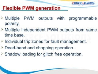
- 36. Flexible PWM generation Multiple PWM outputs with programmable polarity. Multiple independent PWM outputs from same time base. Individual trip zones for fault management. Dead-band and chopping operation. Shadow loading for glitch free operation.
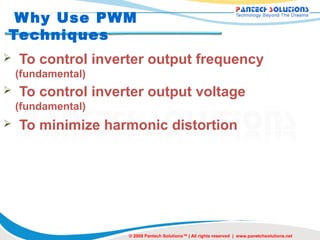
- 37. W hy Use PWM Techniques To control inverter output frequency (fundamental) To control inverter output voltage (fundamental) To minimize harmonic distortion © 2008 Pantech Solutions™ | All rights reserved | www.panetchsolutions.net
- 38. PWM Period & Frequency Calculator PWM period = (TBPRD + 1 ) * TTBCLK for up counter. PWM period = 2 x TBPRD * TTBCLK for UPDOWN © 2008 Pantech Solutions™ | All rights reserved | www.panetchsolutions.net
- 39. Event Manager For Motion control and Motor control applications Modules GP Timers PWMs QEP Capture Units Types EVA EVB © 2008 Pantech Solutions™ | All rights reserved | www.panetchsolutions.net
- 40. Event Manager Signals EVA EVB Modules Module Signal Module Signal GP Timer 1 T1PWM/T1CMP GP Timer 3 T3PWM/T3CMP GP Timers GP Timer 2 T2PWM/T2CMP GP Timer 4 T4PWM/T4CMP Compare 1 PWM1/2 Compare 4 PWM7/8 Compare Modules Compare 2 PWM3/4 Compare 5 PWM9/10 Compare 3 PWM5/6 Compare 6 PWM11/12 Capture 1 CAP1 Capture 4 CAP4 Capture Modules Capture 2 CAP2 Capture 5 CAP5 Capture 3 CAP3 Capture 6 CAP6 QEP1 QEP3 QEP Units QEP QEP2 QEP QEP4 QEPI1 QEP12 Timer- TDIRA Timer- TDIRB direction direction External Timer Interrupts external external clock TCLKINA clock TCLKINB C1TRIP C4TRIP External Compare Output Compare C2TRIP Compare C5TRIP C3TRIP C6TRIP T1CTRIP/ T3CTRIP/ External Trip Inputs T2CTRIP T4CTRIP © 2008 Pantech Solutions™ | All rights reserved | www.panetchsolutions.net
- 41. General-Purpose (GP) Timers Two nos of Timers in Each EV Registers TxCNT Counter Register 16-bit TxCMPR Compare Register 16-bit, Double Buffered and Shadow Register TxPR Period Register 16-bit, Double Buffered and Shadow Register TxCON Timer Control Register TDIRx Direction Register © 2008 Pantech Solutions™ | All rights reserved | www.panetchsolutions.net
- 42. PWM Characteristics 16-bit registers Wide range of programmable dead band for the PWM output pairs Change of the PWM carrier frequency for PWM frequency wobbling as needed. Change of the PWM pulse widths within and after each PWM period as needed. External-maskable power and drive-protection interrupts. Pulse-pattern-generator circuit, for programmable generation of asymmetric, symmetric, and eight-space vector PWM waveforms. Minimized CPU overhead using auto-reload of the compare and period registers. © 2008 Pantech Solutions™ | All rights reserved | www.panetchsolutions.net
- 43. Generating PWM Step1 Select Event Manager EVA or EVB or both; Step2 Initialize the Timer1 Period Compare Counter Step3 Initialize the Timer2 Period Compare Counter © 2008 Pantech Solutions™ | All rights reserved | www.panetchsolutions.net
- 44. Generating PWM Step4 Initialize the General purpose Timer Control Register A Step5 Enable Compare Register Step6 Setup compare action control register © 2008 Pantech Solutions™ | All rights reserved | www.panetchsolutions.net
- 45. Example Code EvaRegs.T1PR = 0xFFFF; // Timer1 period EvaRegs.T1CMPR = 0x3C00; // Timer1 compare EvaRegs.T1CNT = 0x0000; // Timer1 counter EvaRegs.T1CON.all = 0x1042; EvaRegs.T2PR = 0x0FFF; // Timer2 period EvaRegs.T2CMPR = 0x03C0; // Timer2 compare EvaRegs.T2CNT = 0x0000; // Timer2 counter EvaRegs.T2CON.all = 0x1042; EvaRegs.GPTCONA.bit.TCMPOE = 1; EvaRegs.GPTCONA.bit.T1PIN = 1; EvaRegs.GPTCONA.bit.T2PIN = 2; EvaRegs.CMPR1 = 0x0C00; EvaRegs.CMPR2 = 0x3C00; EvaRegs.CMPR3 = 0xFC00; EvaRegs.ACTRA.all = 0x0666; EvaRegs.DBTCONA.all = 0x0000; // Disable deadband EvaRegs.COMCONA.all = 0xA600; © 2008 Pantech Solutions™ | All rights reserved | www.panetchsolutions.net
- 46. Advancement of PWM features in DSP processor © 2008 Pantech Solutions™ | All rights reserved | www.panetchsolutions.net
- 47. EPWM Block Time-base (TB) module Counter-compare (CC) module Action-qualifier (AQ) module Dead-band (DB) module PWM-chopper (PC) module Event-trigger (ET) module Trip-zone (TZ) module
- 48. EPWM Time-Base Count Modes
- 49. EPWM Compare Event Waveforms
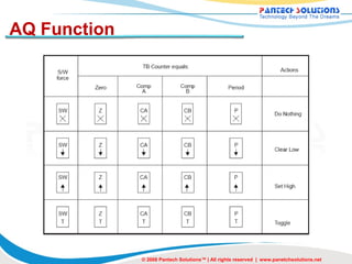
- 50. AQ Function © 2008 Pantech Solutions™ | All rights reserved | www.panetchsolutions.net
- 51. EPWM Count Up Asymmetric Waveform with Independent Modulation on EPWMA / B
- 52. Motivation for Dead-Band Supply Rail Gate Signal Complementary PWM To power Switching Device Transistor gates turn on faster than they shut off Short circuit if both gates are on at same time!
- 54. ePWM Event-Trigger Interrupts and SOC
- 55. High Resolution PWM (HRPWM) PWM Period Regular PWM Device Clock Step (i.e. 100MHz) (i.e. 10ns) HRPWM divides a clock Calibration Logic tracks the cycle into smaller steps number of Micro Steps per ms ms ms ms ms ms called Micro Steps clock to account for (Step Size ~= 150ps) Calibration Logic variations caused by Temp/Volt/Process HRPWM Micro Step (~150ps)
- 56. References 1.http://www-k.ext.ti.com/sc/technical_support/knowledgebase.htm 2.TMS320x2833x, 2823x Enhanced Pulse Width Modulator (ePWM) Module 3.TMS320C28x Assembly Language Tools v5.0.0 4.TMS320C28x CPU and Instruction Set Reference Guide 5. TMS320F28335/28334/28332 TMS320F28235/28234/28232 Digital Signal Controller 6.www.pantechforum.com © 2009 Pantech Solutions™ | All rights reserved | www.panetchsolutions.net
- 57. ANY ? © 2008 Pantech Solutions™ | All rights reserved | www.panetchsolutions.net
Editor's Notes
- #2: Linker command file allows you to configure system memory by allocating output section efficiently in to the memory map.