Architecture of the Intel 8051 Microcontroller
Download as PPTX, PDF3 likes6,585 views

The document provides a comprehensive overview of the architecture and functionality of the 8051 microcontroller, including its memory organization, registers, and I/O ports. It discusses various families of microcontrollers, the key architectural features, and the 8051's specific characteristics such as its instruction set and operation in embedded systems. Additionally, the document outlines memory allocation, instruction execution, and details about special function registers essential for programming the 8051 microcontroller.


![SFRs in 8051
Accumulator(A or ACC) and B register – 8 bit each
DPTR - [DPH:DPL] – 16 bit combined
PC : Program Counter – 16 bits
Stack pointer SP – 8 bit
PSW : Program Status Word
Port Latches
Serial Data Buffer
Timer Registers
Control Registers](https://image.slidesharecdn.com/eslect2-180226181633/85/Architecture-of-the-Intel-8051-Microcontroller-26-320.jpg)


![SFRs in 8051
The DPL and DPH Registers
The 2 8-bit registers that can be combined into a 16-
bit DPTR
Used as Data pointer to access external memory
– mov DPTR, #data16 ; setup DPTR with 16bit external address
– movx A, @DPTR ; copy mem[DPTR] to A
(Other examples: MOVC A,@A+DPTR MOVX A,@DPTR MOVX @DPTR,A )
Can be accessed as 2 separate 8-bit registers if
needed.
– mov DPL, #data8](https://image.slidesharecdn.com/eslect2-180226181633/85/Architecture-of-the-Intel-8051-Microcontroller-29-320.jpg)


Architecture of the Intel 8051 Microcontroller
- 1. 8-15TH JANUARY 2018 Architecture of the 8051 Microcontroller Sudhanshu Janwadkar, TA, SV National Institute of Technology, Surat
- 2. Learning Objectives Getting started with Microcontrollers Study Architecture of 8051 Microcontroller Understand 8051 Registers Learn Pin Diagram and function of each pin Understand On-Chip ROM Address Range, RAM Allocation, Memory Bank and SFRs Learn concept of Program and Data Memory Study I/O Ports Study Stack
- 3. Microcontrollers can be considered as self-contained systems with a processor, memory and I/O ports. In most cases, all that is missing is the software to define the operation of the embedded system Getting Started with Microcontrollers
- 4. The Architectural Needs of a Microcontroller What architectural features might be needed in a microcontroller? What are the expected applications? – Sensing the environment > Input port/pins – Producing a response > Output port/pins – The response may be delayed > Timer/Counter – Prioritized response may be expected > Interrupts – Software to control the process > Non-volatile Memory – Temporary data > RAM.
- 5. Microcontroller Families There are several major “families” of microcontrollers available from different manufacturers. A family is defined as a group of products that share the same basic internal architectures and who are code- compatible. Manufacturers usually define an architecture and then make variants of that design producing a family of products. Code written for a member of the family should be compatible with all other members of the same family.
- 6. Example: Comparison of 8051 Family Members
- 7. Microcontrollers compatible with Intel 8051 Atmel: AT89C51, AT89S51, AT83C5134 Infineon: XC800 Mentor Graphics: M8051ew Megawin: 74, 82, 84, 86, 87, and 89 series NXP: NXP700 and NXP900 series Silicon Labs: C8051 series Texas Instruments: CC111x, CC24xx and CC25xx STC Micro: STC89C51RC, STC90C51RC etc That would imply: All these Microcontrollers share common architecture and Instruction Set
- 8. Intel 8051 (MCS-51) The Intel MCS-51 (commonly termed 8051) is an internally Harvard architecture Complex instruction set computer (CISC) Instruction set single chip microcontroller (µC) series developed by Intel in 1980 for use in embedded systems.
- 9. Common Features of MCS51 Originally introduced by Intel in 1981. Currently, the most widely studied 8-bit microcontroller. 2 distinct separately addressable memory areas. • Maximum of 64K on-chip ROM • Maximum of 64K external data memory • Maximum of 64K external code memory Basic version (8051) contains: • 4K Bytes of on-chip ROM instruction memory • 256 Bytes of On-chip RAM - (128) Bytes of on-chip RAM for temporary data storage and the stack + (128) SFR space • 2 timers, one serial port, and four 8-bit parallel I/O ports. • Speeds starting from ~12 MHz
- 10. Block Diagram of MCS-51
- 11. MCS51 Architecture Programmer’s View – Memory Organization – Register Set – Instruction Set Hardware Designer’s View – Pin Configurations – Timing characteristics – Current / Voltage requirements
- 12. Memory Organisation of MCS-51 The 8051 has separate address spaces for program storage and data storage. Depending on the type of instruction, the same address can refer to two logically & physically different memory locations.
- 13. Memory Organisation of MCS-51 Program Memory After reset, the MCS-51 starts fetching instructions from 0000H. This can be either on-chip or external depending on the value of the EA input pin. • We connect the EA pin to Vcc to indicate that the program code is stored in the microcontroller’s on-chip ROM. • To indicate that the program code is stored in external ROM, EA pin must be connected to GND.
- 14. To use external program memory, All we have to do is to connect the EA pin to ground and connect the (microcontroller) chip to external ROM containing the program code
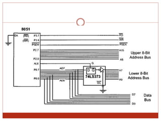
- 16. Since the PC (program counter) of the 8051 is 16-bit, it is capable of accessing up to 64K bytes of program code. In the 8051, port 0 and port 2 provide the 16-bit address to access external memory. Of these two ports, PO provides the lower 8 bit addresses AO – A7, and P2 provides the upper 8 bit addresses A8 – A15. More importantly, PO is also used to provide the 8-bit data bus DO – D7. In other words, pins PO.O – P0.7 are used for both the address and data paths. This is called address/data multiplexing in chip design
- 17. How do we know when P0 is used for the data path and when it is used for the address path? This is the job of the ALE (address latch enable) pin. When ALE = 0 the 8051 uses P0 for the data path, and when ALE = 1, it uses it for the address path. To extract the addresses from the P0 pins we connect P0 to a latch and use the ALE pin to latch the address
- 19. Program Memory(External Access Cycle) Port 0 acts as a multiplexed address/data bus sending the low byte of the program counter (PCL) as an address(through latch) Port 2 sends the program counter high byte of the program counter (PCH) as an address directly to the external memory. The signal ALE allows an external latch to store the PCL byte while the multiplexed bus is made ready to receive the code byte from the external memory. Port 0 then switches function and becomes the data bus receiving the byte from memory
- 20. Memory Organisation of MCS-51 The Lower 128 bytes house the 8051’s registers, its default stack area, and other features. The 8051 has 256 bytes of RAM on-chip. – The lower 128 bytes are intended for internal data storage. – The upper 128 bytes are the Special Function Registers (SFRs). Data Memory
- 21. Memory Organisation of MCS-51 Data Memory The lowest 32 bytes of the on-chip RAM form 4 banks of 8 registers each. – Only one of these banks can be active at any time. – Bank is chosen by setting 2 bits in PSW – Default bank (at power up) is Bank 0 The 8 registers in any active bank are referred to as R0 through R7 Given that each register has a specific address, it can be accessed directly using that address even if its bank is not the active one
- 22. Memory Organisation of MCS-51 Data Memory The next 16 bytes – locations 20H to 2FH – form a block that can be addressed as either bytes or individual bits. Locations 30H to 7FH are general purpose RAM. – The bytes have addresses 20H to 2FH. – The bits have addresses 00H to 7FH. – Specific instructions are used for accessing the bits.
- 23. Memory Organisation of MCS-51 Data Memory The Lower 128 bytes
- 24. Memory Organisation of MCS-51 SFRs The upper 128 bytes of the on-chip RAM are used to house Special Function Registers. In reality, only about 21 of these bytes are actually used. (The others are reserved for future versions of the 8051.) – These are registers associated with important functions in the operation of the MCS-51. – Some of these registers are bit-addressable as well as byte-addressable. The address of bit 0 of the register will be the same as the address of the register.
- 25. Memory Organisation of MCS-51 SFRs
- 26. SFRs in 8051 Accumulator(A or ACC) and B register – 8 bit each DPTR - [DPH:DPL] – 16 bit combined PC : Program Counter – 16 bits Stack pointer SP – 8 bit PSW : Program Status Word Port Latches Serial Data Buffer Timer Registers Control Registers
- 27. SFRs in 8051 Accumulator Almost all the data transfer& arithmetic instructions involve accumulator Can be referred to in several ways: – Implicitly in opcodes. – Referred to as ACC (or A) for instructions that allow specifying a register. – By its SFR address 0E0H. Bit addressable. – ACC.2 means bit 2 of the ACC register
- 28. SFRs in 8051 The B Register The B register is not frequently used, when used it acts as a temporary register, much like a 9th R register. Used Specifically by two instructions – mul AB – div AB Here, B register holds the second operand initially and will hold part of the result after the execution of instruction – It houses upper 8 bits of the multiplication result – It houses Remainder in case of division. Can also be accessed through its SFR address of 0F0H. Bit addressable
- 29. SFRs in 8051 The DPL and DPH Registers The 2 8-bit registers that can be combined into a 16- bit DPTR Used as Data pointer to access external memory – mov DPTR, #data16 ; setup DPTR with 16bit external address – movx A, @DPTR ; copy mem[DPTR] to A (Other examples: MOVC A,@A+DPTR MOVX A,@DPTR MOVX @DPTR,A ) Can be accessed as 2 separate 8-bit registers if needed. – mov DPL, #data8
- 30. SFRs in 8051 The Stack Pointer SP points to the last used location of the stack. – Push operation will first increment SP and then copy data. –Pop operation will first copy data and then decrement SP. In 8051, stack grows upwards (from low memory to high memory) and can be in the internal RAM only. On power-up, SP points to 07H. – Register banks 2,3,4 (08H to 1FH) form the default stack area. Stack can be relocated by setting SP to the upper memory area in 30H to 7FH. – mov SP, #32H
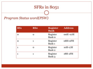
- 31. SFRs in 8051 Program Status word(PSW) CY AC F0 RS1 RS0 OV - P Bit position Function CY PSW.7 Carry Flag AC PSW.6 Auxiliary Carry Flag, for BCD Operations F0 PSW.5 Flag 0. Available to the user for general purposes. RS1 PSW.4 Register bank select bits. Set by software to determine which register bank is being used.RS0 PSW.3 OV PSW.2 Overflow Flag - PSW.1 Reserved P PSW.0 Parity Flag
- 32. SFRs in 8051 Program Status word(PSW) RS1 RS0 Register Bank Address 0 0 Register Bank 0 00H -07H 0 1 Register Bank 1 08H-0FH 1 0 Register Bank 2 10H-17H 1 1 Register Bank 3 18H-1FH
- 33. CY, the carry flag This flag is set whenever there is a carry out from the D7 bit. This flag bit is affected after an 8-bit addition or subtraction. It can also be set to 1 or 0 directly by an instruction such as “SETB C” and “CLR C” where “SETB C” stands for “set bit carry” and “CLR C” for “clear carry”. AC, the auxiliary carry flag If there is a carry from D3 to D4 during an ADD or SUB operation, this bit is set; otherwise, it is cleared. This flag is used by instructions that perform BCD (binary coded decimal) arithmetic. P, the parity flag The parity flag reflects the number of 1’s in the A (accumulator) register only. If the A register contains an odd number of Is, then P = 1. Therefore, P = 0 if A has an even number of 1’s. OV, the overflow flag This flag is set whenever the result of a signed number operation is too large, causing the high-order bit to overflow into the sign bit. The overflow flag is only used to detect errors in signed arithmetic operations.
- 37. SFRs in 8051 Port Latches (P0,P1,P2,P3) Specify the value to be output on the specific output port or the value read from the specific input port. Bit addressable. First bit has the same address as the register. – Example: P1 has address 90H in the SFR, so P1.7 or 97H refer to the same bit
- 38. SFRs in 8051 The SBUF Register Serial Port Data Buffer. 2 registers at the same location One is read-only used for reading serial input data: Serial Data Receive Buffer. The other is write-only used for storing serial output data: Serial Data Transmit Buffer
- 39. SFRs in 8051 Timer Registers – TH0 and TL0 The high and low bytes of the 16-bit counting register for timer/counter T0. There is also a TH1 / TL1 pair for the T1 timer. In the 8052, one more pair exists (TH2) / (TL2) for the T2 timer.
- 40. SFRs in 8051 Control Registers IP – Interrupt Priority IE – Interrupt Enable TMOD – Timer Mode TCON – Timer Control T2CON – Timer 2 Control (8052) SCON – Serial Port Control PCON – Power Control
- 41. Program Counter(PC) PC is not a SFR!! PC is a 16-bit register (consist of PCL and PCH- 8bits each) PC is the only register which does not have an internal address PC holds the address of next instruction to be executed PC automatically increments (+1) after every instruction byte is fetched