SlideShare a Scribd company logo
2 8085 microprocessor
8085 MICROPROCESSOR


    used to store data temporarily during the execution of a program and are
    accessible to the user through instructions.
•   Control Unit: The control unit provides the necessary timing and control signals
    to all the operations in the microcomputer. It controls the flow of data between
    the microprocessor and memory and peripherals.
•   Memory: Memory stores such binary information as instructions and data, and
    provides that information to the microprocessor whenever necessary. To execute
    programs, the microprocessor reads instructions and data from memory and
    performs the computing operations in its ALU section. Results are either
    transferred to the output section for display or stored in memory for later use.
    Read-Only memory (ROM) and Read/Write memory (R/WM), popularly known as
    Random- Access memory (RAM).
           o The ROM is used to store programs that do not need alterations. The
               monitor program of a single-board microcomputer is generally stored
               in the ROM. This program interprets the information entered through a
               keyboard and provides equivalent binary digits to the microprocessor.
               Programs stored in the ROM can only be read; they cannot be altered.
           o   The Read/Write memory (R/WM) is also known as user memory. It is
               used   to   store   user   programs     and    data.    In   single-board
               microcomputers, the monitor program monitors the Hex keys and
               stores those instructions and data in the R/W memory. The information
               stored in this memory can be easily read and altered.
•   I/O (Input/output): It communicates with the outside world. I/O includes two
    types of devices: input and output; these I/O devices are also known as
    peripherals.
•   System Bus: The system bus is a communication path between the micro-
    processor and peripherals: it is nothing but a group of wires to carry bits.

Q. What are different applications of Microprocessor?

Applications of Microprocessor include

    •   Actuator control systems: speed, velocity, acceleration control of electric
        motor, fluid power actuators.
© Rohan Desai- Automobile Dept- New Polytechnic, Kolhapur                          Page 2
8085 MICROPROCESSOR


   •   Control system for home appliances: microwave oven, washing machine,
       refrigerator, heating system, air conditioner (AC), etc.
   •   Control system for computer peripherals: Disk drives, printers, keyboard,
       modem and so on
   •   Automobile control system: Engine control, locking system, monitoring
       systems
   •   Traffic control systems: Road, air and ocean traffic, navigation, etc.
   •   Machine control systems: Robotics, mobile robotics, crane, Automated Guided
       Vehicle (AGV), Numeric Control (NC) machine
   •   Production lines: Assembly lines, packaging systems, bottling plant, etc.

Q. Explain 8085 Bus structure.

Address Bus:
   •   The address bus is a group of 16 lines generally identified as A0 to A15.
   •   The address bus is unidirectional: bits flow in one direction - from the
       microprocessor to peripheral devices.
   •   The microprocessor uses the address bus to perform the first function:
       identifying a peripheral or a memory location.
Data Bus:
   •   The data bus is a group of eight lines used for data flow.
   •   These lines are bi-directional - data flow in both directions between the
       microprocessor and memory and peripheral devices.
   •   The microprocessor uses the data bus to perform the second function:
       transferring binary information.
   •   The largest number that can appear on the data bus is 11111111.
Control Bus:
   •   The control bus carries synchronization signals and providing timing signals.
   •   The MPU generates specific control signals for every operation it performs.
   •   These signals are used to identify a device type with which the MPU wants to
       communicate.


© Rohan Desai- Automobile Dept- New Polytechnic, Kolhapur                          Page 3
2 8085 microprocessor
8085 MICROPROCESSOR


Flags

The flag register in the microprocessor is a special purpose register in which the
individual bit values represent the standing of a result byte. The flag bits are
automatically modified in accordance with the result. The flag bits in many situations
are important than result itself. The programmer, when necessary, uses the tested
and recorded flag bits. A thorough understanding of flags is essential in writing
assembly language programs.

There are five flag bits: Zero (Z), Carry (CY), Sign (S), Parity (P), and Overflow (V)
flags.


Flag        Set i.e. 1                       Reset i.e. 0
Z           Result is zero                   Result is non-zero
CY          Carry is generated               Carry is not generated
S           Result is negative               Result is positive
P           Result has even number of 1s     Result has odd number of 1s
V           Overflow occurs                  Overflow does not occur


Instruction Decoder or Microcode Engine

This is the main unit, which is responsible for decoding the instructions. The
instructions (OPCODE) fetched from the memory are placed in the IR. Once the
OPCODE enters into the microprocessor, it must be decoded in order to generate
control signals for ‘what to do next’. A unique set of control signal is generated
according to the instruction types. For instance, if it is an instruction (OPCODE) for
addition, then addition related control signals are produced. If the OPCODE is a
comparison instruction, then addition related control signals are produced.

Stack and Stack Pointer (SP)

Stack is a user-defined memory space, which includes many locations within the
memory space of the microprocessor. These memory locations are special in the
sense that when interrupts occur, the microprocessor stores the current content of
the various registers and flags in the stack in order to attend the interrupt.
Microprocessor is presently doing some task (executing some codes). In the
meantime, the interrupt has occurred. The microprocessor must listen, or attend, to
the interrupt while suspending the present task. Attending to interrupt implies
execution of another sub-task or sub-program corresponding to interrupt. The sub-
task is referred to as subroutine. The control, or the Program Counter, will hold the
address of another location corresponding to this interrupt.


© Rohan Desai- Automobile Dept- New Polytechnic, Kolhapur                       Page 8
2 8085 microprocessor
8085 MICROPROCESSOR

Figure shows the logic pinout of the 8085 microprocessor. All the signals can be
classified into six groups: (1) address bus, (2) data bus, (3) control and status
signals, (4) power supply and frequency signals, (5) externally initiated signals, and
(6) serial I/O ports.

ADDRESS BUS

The 8085 has 16 signal lines (pins) that are used as the address bus; however,
these lines are split into two segments: A15-A8 and AD7-AD0. The eight signal lines,
A15-A8, are unidirectional and used for the most significant bits, called the high-order
address, of a 16-bit address. The signal lines AD7-AD0 are used for a dual purpose,
as explained in the next section.

MULTIPLEXED ADDRESS / DATA BUS

The signal lines AD7-AD0 are bidirectional: they serve dual purpose. They are used as
the low-order address bus as well as the data bus. In executing an instruction,
during the earlier part of the cycle, these lines are used as the low-order address
bus. During the later part of the cycle, these lines are used as data bus.

CONTROL AND STATUS SIGNALS

This group of signals includes two control signals (RD and WR), three status signals
(IO/M, S1, and S0) to identify the nature of the operation, and one special signal
(ALE) to indicate the beginning of the operation. These signals are as follows:

   •   ALE – Address Latch Enable. This is positive going pulse generated every time
       the 8085 begins an operation (machine cycle); it indicates that the bits on
       AD7-AD0 are address bits. This signal is used primarily to latch the low-order
       address from the multiplexed bus and generate a separate set of eight
       address lines, A7-A0.
   •   RD - Read. This is Read control signal (active low). This signal indicates that
       ¯¯
       the selected I/O or memory device is to be read and data is available on the
       data bus.
   •   WR - Write. This is a Write control signal (active low). This signal indicates
        ¯¯
       that the data on the data bus are to be written into a selected memory or I/O
       location.
   •   IO/¯¯ - This is a status signal used to differentiate between I/O and memory
           M
       operations. When it is high, it indicates an I/O operation; when it is low, it
       indicates a memory operation.
   •   S1 and S0 – These are status signals, similar to IO/¯¯ , can identify various
                                                              M
       operations, but they are rarely used in small systems.


© Rohan Desai- Automobile Dept- New Polytechnic, Kolhapur                       Page 11
8085 MICROPROCESSOR


POWER SUPPLY AND CLOCK FREQUENCY

The power supply and frequency signals are as follows:

   •   Vcc - +5 V power supply
   •   Vss – Ground Reference
   •   X1, X2 – A crystal is connected at these two pins.
   •   CLK (OUT) – Clock Output. This signal can be used as the system clock for
       other devices.

EXTERNALLY INITIATED SIGNALS INCLUDING INTERRUPTS

The 8085 has five interrupt signals that can be used to interrupt program execution.
These are listed in the table below.

                    Interrupt Request: This is used as a general purpose interrupt.
   INTR (Input)
                    It has lowest priority.
                    Interrupt Acknowledge: This is used to acknowledge an
   INTA (Output)
   ¯¯¯¯
                    interrupt.
   RST 7.5 (Inputs) Restart Interrupts: These are vectored interrupts that transfer
   RST 6.5          the program control to specific memory locations. Among
   RST 5.5          these three priority order is 7.5, 6.5, 5.5
   TRAP (Input)       This interrupt has highest priority.


TRAP is the only non-maskable interrupt i.e. it cannot be enabled or disabled by
program. Other interrupts (INTR and Restart interrupts) are maskable i.e. they can
be enabled or disabled using programs.

In addition to the interrupts, three pins – RESET, HOLD, and READY- accept
externally initiated signals as input.

                      This signal indicates that a peripheral such as DMA (Direct
   HOLD (Input)       Memory Access) controller is requesting the use of address
                      and data buses.
                      Hold Acknowledge: This signal acknowledges the HOLD
   HLDA (Output)
                      request.
                      READY is used by the microprocessor to check whether a
                      peripheral is ready to accept or transfer data. If READY is high
   READY (Input)
                      then the peripheral is ready for data transfer. If not the
                      microprocessor waits until READY goes high.
   RESET ¯¯
   ¯¯¯¯¯ IN           When the signal on this pin goes low, microprocessor is reset.
   RESET OUT          This signal indicates that microprocessor is being reset.


© Rohan Desai- Automobile Dept- New Polytechnic, Kolhapur                         Page 12
8085 MICROPROCESSOR


SERIAL I/O PORTS

The 8085 has two signals to implement the serial transmission: SID (Serial Input
Data) and SOD (Serial Output Data). In serial transmission, data bits are sent over a
single line, one bit at a time, such as the transmission over telephone lines.


Q. What do you understand by Instruction and Program?

Instruction means a command in binary that is recognized and executed by the
microprocessor to accomplish a task.

Program is a set of instructions written in a specific sequence for microprocessor to
accomplish a given task.

Q. What do you understand by Machine Language and Assembly
Language?

   •   Microprocessors recognize and operate in binary numbers. Each
       microprocessor has its own set of instructions. An instruction is combination
       of 0s and 1s.
   •   To communicate with the microprocessor, one must give instructions in binary
       language. This language is called machine language.
   •   But it is very difficult and error prone to write programs in machine language
       because it is just a series of 0s and 1s and instructions are not easily
       comprehended by just looking at the pattern.
   •   To overcome this difficulty, computer manufacturers have devised English-like
       words to represent the binary instructions of microprocessor. Programmers
       can write programs using these words. This language is called assembly
       language.
   •   For example 0011 1100 is an instruction in machine language that increments
       the number in accumulator by one. The same instruction is represented by
       INR A in assembly language.

Q. What do you mean by low level language and high level language?

   •   The machine language and assembly language are microprocessor specific
       languages.
   •   Therefore they are called as low level languages.
   •   The programs written in these languages are not transferrable from one
       machine to another.
   •    To overcome this limitation, such general purpose languages as BASIC,
       FORTRAN, and C have been devised. A program written in these languages is
       machine independent. Such languages are called high level languages.

© Rohan Desai- Automobile Dept- New Polytechnic, Kolhapur                     Page 13
8085 MICROPROCESSOR


Q. Explain the term mnemonic.

   •    Microprocessor instructions are in the binary form. Since the program written
        in binary instructions is difficult to understand, each manufacturer of a
        microprocessor has devised a symbolic code for each instruction. This
        symbolic code is called mnemonic.
   •    The mnemonic for a particular instruction consists of letters that suggest the
        operation to be performed by that instruction.
   •    For example, the binary code 0011 1100 (3CH in hexadecimal) of the 8085
        microprocessor is represented by the mnemonic INR A. This instruction
        increments accumulator contents by one.
   •    Similarly, the binary code 1000 0000 (80H) is represented by mnemonic ADD
        B. ADD stands for addition and B represents the contents in register B. This
        instruction performs addition of contents of B and contents of accumulator.


Q. Explain the terms Opcode and operand.

    •   An instruction is a command to the microprocessor to perform a given task
        on specified data.
    •   Each instruction has two parts: one is the task to be performed, called the
        operation code (Opcode), and the second is the data to be operated on,
        called the operand.
    •   The operand (or data) can be specified in various ways. It may include 8-bit
        (or 16-bit) data, an internal register, a memory location, or address. In some
        instructions, the operand is implicit.

Q. Explain the term Assembler.

   •    Writing programs in machine language is very difficult and error prone to
        write programs in machine language because it is just a series of 0s and 1s
        and instructions are not easily comprehended by just looking at the pattern.
   •    To overcome this difficulty, computer manufacturers have devised English-like
        words to represent the binary instructions of microprocessor. Programmers
        can write programs using these words. This language is called assembly
        language.
   •    Assembler is a computer program which translates an assembly language
        program to machine language program.
   •    Programmer writes program in assembly language in the form of mnemonics.
        He then enters that assembly language program into assembler by using the
        ASCII keyboard. Assembler converts this program into binary machine code.
   •    Since machine language is machine dependent, each microprocessor has its
        own assembler.

© Rohan Desai- Automobile Dept- New Polytechnic, Kolhapur                      Page 14
2 8085 microprocessor
8085 MICROPROCESSOR


Arithmetic operations

These instructions perform arithmetic operations such as addition, subtraction,
increment and decrement.

Logical operations

These instructions perform various logical operations such as AND, OR, EX-OR,
Compare, Compliment, etc.

Branching operations

These instructions alter the sequence f program execution either conditionally or
unconditionally.

Machine Control operations

These instructions control machine functions such as Halt, Interrupt, etc.

Q. How are 8085 instructions classified according to word size?

The 8085 instruction set is classified into following three groups according to word
size or byte size.

   •   1-byte instructions
   •   2-byte instructions
   •   3-byte instructions

ONE-BYTE INSTRUCTIONS

A 1-byte instruction includes the Opcode and the Operand in the same byte. For
example

              Task                Opcode      Operand       Binary Code      Hex Code
Copy contents of accumulator       MOV          C, A         0100 1111         4FH
in register C


TWO-BYTE INSTRUCTIONS

In a 2-byte instruction, the first byte specifies the operation code and the second
byte specifies the operand. For example

             Task                 Opcode      Operand       Binary Code      Hex Code
Load 8-bit data byte in the        MVI         A, 32H        0011 1100          3E
accumulator                                                  0011 0010          32


© Rohan Desai- Automobile Dept- New Polytechnic, Kolhapur                      Page 16
8085 MICROPROCESSOR


THREE-BYTE INSTRUCTION

In a 3-byte instruction, the first byte specifies the Opcode, and the following two
bytes specify the 16-bit address. Note that the second byte is the low-order address
and the third byte is the higher-order address. For example

             Task                     Opcode     Operand     Binary Code     Hex Code
Load contents of memory                LDA        2050H       0011 1010         3A
2050H into A                                                  0101 0000         50
                                                              0010 0000         20


Q. Explain these terms: SSI, MSI and LSI.

       •    SSI (small-scale integration): the process of designing a few circuits on a
            single chip. The term refers to the technology used to fabricate discrete
            logic gates on a chip.
       •    MSI (medium-scale integration): the process of designing more than a
            hundred gates on a single chip.
       •    LSI (large-scale integration): the process of designing more than a thousand
            gates on a single chip.


Q. Explain Fetch Cycle and Write Cycle.

Fetch Cycle: The microprocessor fetches the OPCODE or data from the memory or
input devices as follows. The content of the PC, the address is placed in the MAR.
The content of the MAR is then transferred to the decoder, which is interfaced or in
built with the memory device. The decoder decodes the address, and selects the
appropriate location according to the address supplied to it. The content of the
specified address is read and transferred into the microprocessor. If the item read is
an OPCODE, then it is placed in the Instruction Register, and if the item read is data,
then it is placed in the Data Register. This is a fetch cycle or memory read cycle. In
particular following events are carried out within a fetch cycle:

   •       Send address through address bus
   •       Decode the address
   •       Read the content of the specified location
   •       Transfer the content of the specified location in the memory to the micro-
           processor.


© Rohan Desai- Automobile Dept- New Polytechnic, Kolhapur                        Page 17
8085 MICROPROCESSOR

Write Cycle: Write cycle is one that interprets writing operation. Microprocessor can
send data to a specific location of the memory or to an output device. During writing
operation, the microprocessor transfers the contents of the PC to the memory
decoder through MAR. The microprocessor uses WR (write) signal for writing into
                                                    ¯¯
the memory.


Q. What do you mean by addressing modes? Explain the different types of
addressing modes in Intel 8085 with examples.

          •   Every instruction of a program has to operate on a data.
          •   The method of specifying the data to be operated by the instruction is
              called Addressing.

The 8085 has the following 5 different types of addressing.

     1.   Immediate Addressing
     2.   Direct Addressing
     3.   Register Addressing
     4.   Register Indirect Addressing
     5.   Implied Addressing

Immediate Addressing:

     •    In immediate addressing mode, the data is specified in the instruction itself.
          The data will be a part of the program instruction.
     •    For example MVI B, 3EH - Move the data 3EH given in the instruction to B
          register.

Direct Addressing:

 •       In direct addressing mode, the address of the data is specified in the
         instruction. The data will be in memory.
 •       For example LDA 1050H - Load the data available in memory location 1050H in
         to accumulator.

Register Addressing:

     •    In register addressing mode, the instruction specifies the name of the register
          in which the data is available.
     •    For example MOV A, B - Move the content of B register to A register.


© Rohan Desai- Automobile Dept- New Polytechnic, Kolhapur                        Page 18
8085 MICROPROCESSOR


Register Indirect Addressing:

   •   In register indirect addressing mode, the instruction specifies the name of the
       register in which the address of the data is available. Here the data will be in
       memory and the address will be in the register pair.
   •   For example MOV A, M - The memory data addressed by H L pair is moved to
       A register.

Implied Addressing:

   •   In implied addressing mode, the instruction itself specifies the data to be
       operated.
   •   For example CMA - Complement the content of accumulator.


Q. What is meant by interfacing of microprocessor?

   •   A microprocessor would not be of much use by itself. To perform useful work
       it needs to be connected to other electronic components. For example, for a
       computer to work, a microprocessor must be interfaced to main memory, a
       graphic subsystem, disk memory, the keyboard and USB ports, etc.
   •   There are two types of interfacing
           o Memory interfacing
           o I/O interfacing
   •   Memory interfacing: While executing an instruction, there is a necessity for
       the microprocessor to access memory frequently for reading various
       instruction codes and data stored in the memory. The primary function of a
       memory interfacing circuit is to aid the microprocessor in reading and writing
       a data to the given register of a memory chip.
   •   I/O Interfacing: We know that keyboard and Displays are used as
       communication channel with outside world. So it is necessary that we
       interface keyboard and displays with the microprocessor. This is called I/O
       interfacing.
   •   INTEL has developed some programmable peripheral devices for processors
       like 8085 for interfacing purpose. The peripheral devices includes

          o 8255 – Parallel Communication Interface (PPI)
          o 8251 – Serial communication Interface (USART- Universal
            Synchronous/Asynchronous Receiver/Transmitter)
          o 8257 – DMA Controller
          o 8279 – Keyboard/Display Controller
          o 8259 – Programmable Interrupt controller
          o 8254 – Programmable Timer

© Rohan Desai- Automobile Dept- New Polytechnic, Kolhapur                      Page 19
8085 MICROPROCESSOR


Q. What do you mean by Microcontrollers?

   •   Microcontroller is a device that includes microprocessor, memory, I/O ports
       and other peripherals on a single chip, fabricated using VLSI technology.
   •   A digital computer typically consists of three major components: the Central
       Processing Unit (CPU), program and data memory, and Input/output (I/O)
       system.
   •   The CPU controls the flow of information among the components of the
       computer. It also processes the data by performing digital operations.
   •   A microprocessor is a CPU that is compacted into a single chip semiconductor
       device.
   •   A computer built around a microprocessor is called a microcomputer. The
       choice of I/O and memory devices of a microcomputer depends on the
       specific application.
   •   A microcontroller is an entire computer manufactured on a single chip.
       Microcontrollers are usually dedicated devices embedded within an
       application.
   •   Microprocessor itself is not a computer. For a microprocessor to act as control
       system, additional chips are necessary, e.g. memory devices for program and
       data storage and input/output ports to allow it to communicate with the
       external world. The microcontroller is the integration of a microprocessor with
       memory and input/output interfaces, and other peripherals such as timers, on
       a single chip.

Q. Differentiate between Microcontroller and Microprocessor.

             Microcontroller                            Microprocessor
Inbuilt RAM and ROM                         Do not have inbuilt RAM and ROM
Inbuilt timer                               Do not have inbuilt timer
I/O ports are available                     I/O ports are not available, requires
                                            extra devices like 8155 or 8255
Inbuilt serial port                         Do not have inbuilt serial port, requires
                                            extra devices like 8250 or 8251
Separate memory to store program and        Program and data are stored in same
data                                        memory
Many multifunctional pins on the IC         Less multifunctional pins on the IC
Boolean operation i.e. operation on         Boolean operation is not possible directly
individual bits is possible directly
Few instructions to read/write data         Many instructions to read/write data
from/to memory                              from/to memory


© Rohan Desai- Automobile Dept- New Polytechnic, Kolhapur                      Page 20
2 8085 microprocessor
8085 MICROPROCESSOR


Port 0 (P0.1/AD0-P0.7/AD7)

Pins 32 to 39 make up the 8-bit bidirectional I/O port. Additionally it is used as lower
address bus.

Port 1 (P1.0-P1.7)

Pins 1 to 8 make up the 8-bit bidirectional I/O port.

Port 2 (P2.0/A8-P2.7/A15)

Pins 21 to 28 make up the 8-bit bidirectional I/O port.

Additionally it is used as higher order address bus.

Port 3 (P3.0-P3.7)

Pins 10 to 17 make up the 8-bit bidirectional I/O port. Additionally each of these
eight pins also has an alternate function, as detailed in the table below.


              Pin     Name         Alternate Function

             P3.0     RXD          Serial input line
             P3.1     TXD          Serial output line
             P3.2     ¯¯¯¯
                      INT0         External interrupt 0
             P3.3     ¯¯¯¯
                      INT1         External interrupt 1
             P3.4     T0           Timer 0 input
             P3.5     T1           Timer 1 input
             P3.6     WR
                      ¯¯           External data memory write
             P3.7     RD
                      ¯¯           External data memory read


RST

The reset input is on pin 9. This pin is used for resetting the 8051

EA
¯¯

The external access, on pin 31, is used for enabling or disabling the on-chip ROM.
When this pin is high, the 8051 executes instructions in internal ROM. When it is
low, the 8051 will always execute instructions in external memory.


© Rohan Desai- Automobile Dept- New Polytechnic, Kolhapur                        Page 24
8085 MICROPROCESSOR


ALE

The address latch enable is on pin 30. The ALE is used for latching the low byte of
the address into an external register.

PSEN (Program Store Enable)
¯¯¯¯

The program store enable is an output signal on pin 29. This signal is used for
fetching instructions from external code memory.

XTAL1, XTAL2

These are the pins for clock connection.


© Rohan Desai- Automobile Dept- New Polytechnic, Kolhapur                     Page 25

More Related Content

What's hot (20)

PPTX
PIC-18 Microcontroller
ASHISH RANJAN
 
PPTX
Introducion to MSP430 Microcontroller.pptx
Dr.YNM
 
PPT
Error detection and correction codes
GargiKhanna1
 
PPTX
Generation of DSB-SC using Diode Ring Modulator or chopper Modulator.pptx
ArunChokkalingam
 
PPTX
1.instrumentation ii
Bikash Gyawali
 
PPTX
Quantization.pptx
ssuserb9f9c42
 
PPTX
Instruction pipelining
Tech_MX
 
PDF
8051 interfacing
KanchanPatil34
 
PDF
instruction pipeline in computer architecture and organization.pdf
Sandip Ladi
 
PPTX
Timer counter in arm7(lpc2148)
Aarav Soni
 
PDF
Analog communications lab
Vishal kakade
 
PPT
TTL Driving CMOS - Digital Electronic Presentation ALA 2018
Mr. RahüL YøGi
 
PPTX
USART
Islam Samir
 
PDF
Interfacing of 8051 with 8255 Programmable Peripheral Interface.pdf
Srikrishna Thota
 
PPTX
Design of safety and surviellance system for underground coal mines using low...
Mohd Faiz
 
PPTX
LPC 2148 ARM MICROCONTROLLER
sravannunna24
 
PPTX
HEARTBEAT RATE SENSOR USING MICROCONTROLLER
Rinku Meena
 
PPTX
I2C Protocol
Sudhanshu Janwadkar
 
PIC-18 Microcontroller
ASHISH RANJAN
 
Introducion to MSP430 Microcontroller.pptx
Dr.YNM
 
Error detection and correction codes
GargiKhanna1
 
Generation of DSB-SC using Diode Ring Modulator or chopper Modulator.pptx
ArunChokkalingam
 
1.instrumentation ii
Bikash Gyawali
 
Quantization.pptx
ssuserb9f9c42
 
Instruction pipelining
Tech_MX
 
8051 interfacing
KanchanPatil34
 
instruction pipeline in computer architecture and organization.pdf
Sandip Ladi
 
Timer counter in arm7(lpc2148)
Aarav Soni
 
Analog communications lab
Vishal kakade
 
TTL Driving CMOS - Digital Electronic Presentation ALA 2018
Mr. RahüL YøGi
 
Interfacing of 8051 with 8255 Programmable Peripheral Interface.pdf
Srikrishna Thota
 
Design of safety and surviellance system for underground coal mines using low...
Mohd Faiz
 
LPC 2148 ARM MICROCONTROLLER
sravannunna24
 
HEARTBEAT RATE SENSOR USING MICROCONTROLLER
Rinku Meena
 
I2C Protocol
Sudhanshu Janwadkar
 

Viewers also liked (19)

PDF
8085 microprocessor ramesh gaonkar
SAQUIB AHMAD
 
PPTX
8085 microprocessor
Iama Marsian
 
PDF
Timing diag
Student
 
PDF
T-states in microprocessor 8085
yedles
 
PDF
Microprocessor 8085
Dhaval Barot
 
PPT
8085 microprocessor
Radhika Patel
 
PPTX
microprocessor 8085
Shivanshu Purwar
 
PDF
8085 microprocessor Architecture and Pin description
Vijay Kumar
 
PPTX
Microprocessor 8085 Chapter 3
Rishikesh Bhavsar
 
PPTX
8085 full discription
Kartik Kalpande Patil
 
DOC
Introduction to microprocessor notes
SARITHA REDDY
 
PPTX
Microprocessor 8085 architecture ppt. april 2013
harshalata
 
PPTX
Addressing mode & data transfer instruction of 8085
Chinmayee samal
 
PPTX
Architecture of 80286 microprocessor
Syed Ahmed Zaki
 
DOCX
8085 interfacing with memory chips
Srikrishna Thota
 
PPT
Microprocessor 80386
yash sawarkar
 
PPT
8085 Architecture & Memory Interfacing1
techbed
 
PPT
Memory intrface and addrs modes
balbirvirdi
 
8085 microprocessor ramesh gaonkar
SAQUIB AHMAD
 
8085 microprocessor
Iama Marsian
 
Timing diag
Student
 
T-states in microprocessor 8085
yedles
 
Microprocessor 8085
Dhaval Barot
 
8085 microprocessor
Radhika Patel
 
microprocessor 8085
Shivanshu Purwar
 
8085 microprocessor Architecture and Pin description
Vijay Kumar
 
Microprocessor 8085 Chapter 3
Rishikesh Bhavsar
 
8085 full discription
Kartik Kalpande Patil
 
Introduction to microprocessor notes
SARITHA REDDY
 
Microprocessor 8085 architecture ppt. april 2013
harshalata
 
Addressing mode & data transfer instruction of 8085
Chinmayee samal
 
Architecture of 80286 microprocessor
Syed Ahmed Zaki
 
8085 interfacing with memory chips
Srikrishna Thota
 
Microprocessor 80386
yash sawarkar
 
8085 Architecture & Memory Interfacing1
techbed
 
Memory intrface and addrs modes
balbirvirdi
 
Ad

Similar to 2 8085 microprocessor (20)

PPTX
12 mt06ped001
vijaydeepakg
 
PDF
MPMC UNIT-1. Microprocessor 8085 pdf Microprocessor and Microcontroller
RAHUL RANJAN
 
PPTX
8085 microprocessor
GurleenKaur408
 
PPTX
unit 2 microprocesor8085 for advantages disadvatage gtu syllabus.pptx
dravidparmar1
 
PPTX
8085vs8086 microprocessor and their characteristics and functionalities
emonhassan6464
 
PDF
13402lecture3 111204134846-phpapp02
raj kumar
 
PDF
Lecture Notes Microprocessor and Controller Unit2
Murugan146644
 
PPTX
UNIT 1 Microprocessors.pptx
Gowrishankar C
 
PPT
8085
Sunil Dutt
 
PDF
MICROPROCESSOR 8085 WITH PROGRAMS
Sabin Gautam
 
PPTX
Pin Diagram and block diagram 8085 .pptx
YashArya40
 
PPTX
Introduction to 8085 Microprocessor
Ravi Anand
 
PPTX
Unit 2 - Microprocessor & Microcontroller.pptx
Charunnath S V
 
PDF
itft-8085 microprocessor
Shifali Sharma
 
PDF
Microprocessors 8085 architecture
VARUN BABUNELSON
 
PPTX
introduction to microprocessors
sudheerkethamreddy
 
PPTX
8085 architecture
Rishabh Kataria
 
PPTX
Copy of 8085_Microprocessor.pptx MBSD EE
Kirti316234
 
DOC
Microprocessor Basics 8085 Ch-1
Neelam Kapoor
 
12 mt06ped001
vijaydeepakg
 
MPMC UNIT-1. Microprocessor 8085 pdf Microprocessor and Microcontroller
RAHUL RANJAN
 
8085 microprocessor
GurleenKaur408
 
unit 2 microprocesor8085 for advantages disadvatage gtu syllabus.pptx
dravidparmar1
 
8085vs8086 microprocessor and their characteristics and functionalities
emonhassan6464
 
13402lecture3 111204134846-phpapp02
raj kumar
 
Lecture Notes Microprocessor and Controller Unit2
Murugan146644
 
UNIT 1 Microprocessors.pptx
Gowrishankar C
 
MICROPROCESSOR 8085 WITH PROGRAMS
Sabin Gautam
 
Pin Diagram and block diagram 8085 .pptx
YashArya40
 
Introduction to 8085 Microprocessor
Ravi Anand
 
Unit 2 - Microprocessor & Microcontroller.pptx
Charunnath S V
 
itft-8085 microprocessor
Shifali Sharma
 
Microprocessors 8085 architecture
VARUN BABUNELSON
 
introduction to microprocessors
sudheerkethamreddy
 
8085 architecture
Rishabh Kataria
 
Copy of 8085_Microprocessor.pptx MBSD EE
Kirti316234
 
Microprocessor Basics 8085 Ch-1
Neelam Kapoor
 
Ad

Recently uploaded (20)

PPTX
Darren Mills The Migration Modernization Balancing Act: Navigating Risks and...
AWS Chicago
 
PPTX
Building and Operating a Private Cloud with CloudStack and LINBIT CloudStack ...
ShapeBlue
 
PDF
DevBcn - Building 10x Organizations Using Modern Productivity Metrics
Justin Reock
 
PDF
SWEBOK Guide and Software Services Engineering Education
Hironori Washizaki
 
PPTX
Top iOS App Development Company in the USA for Innovative Apps
SynapseIndia
 
PDF
Building Resilience with Digital Twins : Lessons from Korea
SANGHEE SHIN
 
PDF
Ampere Offers Energy-Efficient Future For AI And Cloud
ShapeBlue
 
PDF
Women in Automation Presents: Reinventing Yourself — Bold Career Pivots That ...
DianaGray10
 
PDF
Rethinking Security Operations - SOC Evolution Journey.pdf
Haris Chughtai
 
PDF
Sustainable and comertially viable mining process.pdf
Avijit Kumar Roy
 
PPTX
✨Unleashing Collaboration: Salesforce Channels & Community Power in Patna!✨
SanjeetMishra29
 
PDF
SFWelly Summer 25 Release Highlights July 2025
Anna Loughnan Colquhoun
 
PDF
Wojciech Ciemski for Top Cyber News MAGAZINE. June 2025
Dr. Ludmila Morozova-Buss
 
PDF
Français Patch Tuesday - Juillet
Ivanti
 
PDF
Smart Air Quality Monitoring with Serrax AQM190 LITE
SERRAX TECHNOLOGIES LLP
 
PDF
Shuen Mei Parth Sharma Boost Productivity, Innovation and Efficiency wit...
AWS Chicago
 
PPTX
Extensions Framework (XaaS) - Enabling Orchestrate Anything
ShapeBlue
 
PDF
CloudStack GPU Integration - Rohit Yadav
ShapeBlue
 
PDF
NewMind AI Journal - Weekly Chronicles - July'25 Week II
NewMind AI
 
PDF
Why Orbit Edge Tech is a Top Next JS Development Company in 2025
mahendraalaska08
 
Darren Mills The Migration Modernization Balancing Act: Navigating Risks and...
AWS Chicago
 
Building and Operating a Private Cloud with CloudStack and LINBIT CloudStack ...
ShapeBlue
 
DevBcn - Building 10x Organizations Using Modern Productivity Metrics
Justin Reock
 
SWEBOK Guide and Software Services Engineering Education
Hironori Washizaki
 
Top iOS App Development Company in the USA for Innovative Apps
SynapseIndia
 
Building Resilience with Digital Twins : Lessons from Korea
SANGHEE SHIN
 
Ampere Offers Energy-Efficient Future For AI And Cloud
ShapeBlue
 
Women in Automation Presents: Reinventing Yourself — Bold Career Pivots That ...
DianaGray10
 
Rethinking Security Operations - SOC Evolution Journey.pdf
Haris Chughtai
 
Sustainable and comertially viable mining process.pdf
Avijit Kumar Roy
 
✨Unleashing Collaboration: Salesforce Channels & Community Power in Patna!✨
SanjeetMishra29
 
SFWelly Summer 25 Release Highlights July 2025
Anna Loughnan Colquhoun
 
Wojciech Ciemski for Top Cyber News MAGAZINE. June 2025
Dr. Ludmila Morozova-Buss
 
Français Patch Tuesday - Juillet
Ivanti
 
Smart Air Quality Monitoring with Serrax AQM190 LITE
SERRAX TECHNOLOGIES LLP
 
Shuen Mei Parth Sharma Boost Productivity, Innovation and Efficiency wit...
AWS Chicago
 
Extensions Framework (XaaS) - Enabling Orchestrate Anything
ShapeBlue
 
CloudStack GPU Integration - Rohit Yadav
ShapeBlue
 
NewMind AI Journal - Weekly Chronicles - July'25 Week II
NewMind AI
 
Why Orbit Edge Tech is a Top Next JS Development Company in 2025
mahendraalaska08
 

2 8085 microprocessor

  • 2. 8085 MICROPROCESSOR used to store data temporarily during the execution of a program and are accessible to the user through instructions. • Control Unit: The control unit provides the necessary timing and control signals to all the operations in the microcomputer. It controls the flow of data between the microprocessor and memory and peripherals. • Memory: Memory stores such binary information as instructions and data, and provides that information to the microprocessor whenever necessary. To execute programs, the microprocessor reads instructions and data from memory and performs the computing operations in its ALU section. Results are either transferred to the output section for display or stored in memory for later use. Read-Only memory (ROM) and Read/Write memory (R/WM), popularly known as Random- Access memory (RAM). o The ROM is used to store programs that do not need alterations. The monitor program of a single-board microcomputer is generally stored in the ROM. This program interprets the information entered through a keyboard and provides equivalent binary digits to the microprocessor. Programs stored in the ROM can only be read; they cannot be altered. o The Read/Write memory (R/WM) is also known as user memory. It is used to store user programs and data. In single-board microcomputers, the monitor program monitors the Hex keys and stores those instructions and data in the R/W memory. The information stored in this memory can be easily read and altered. • I/O (Input/output): It communicates with the outside world. I/O includes two types of devices: input and output; these I/O devices are also known as peripherals. • System Bus: The system bus is a communication path between the micro- processor and peripherals: it is nothing but a group of wires to carry bits. Q. What are different applications of Microprocessor? Applications of Microprocessor include • Actuator control systems: speed, velocity, acceleration control of electric motor, fluid power actuators. © Rohan Desai- Automobile Dept- New Polytechnic, Kolhapur Page 2
  • 3. 8085 MICROPROCESSOR • Control system for home appliances: microwave oven, washing machine, refrigerator, heating system, air conditioner (AC), etc. • Control system for computer peripherals: Disk drives, printers, keyboard, modem and so on • Automobile control system: Engine control, locking system, monitoring systems • Traffic control systems: Road, air and ocean traffic, navigation, etc. • Machine control systems: Robotics, mobile robotics, crane, Automated Guided Vehicle (AGV), Numeric Control (NC) machine • Production lines: Assembly lines, packaging systems, bottling plant, etc. Q. Explain 8085 Bus structure. Address Bus: • The address bus is a group of 16 lines generally identified as A0 to A15. • The address bus is unidirectional: bits flow in one direction - from the microprocessor to peripheral devices. • The microprocessor uses the address bus to perform the first function: identifying a peripheral or a memory location. Data Bus: • The data bus is a group of eight lines used for data flow. • These lines are bi-directional - data flow in both directions between the microprocessor and memory and peripheral devices. • The microprocessor uses the data bus to perform the second function: transferring binary information. • The largest number that can appear on the data bus is 11111111. Control Bus: • The control bus carries synchronization signals and providing timing signals. • The MPU generates specific control signals for every operation it performs. • These signals are used to identify a device type with which the MPU wants to communicate. © Rohan Desai- Automobile Dept- New Polytechnic, Kolhapur Page 3
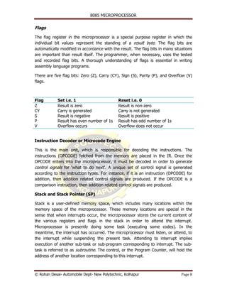
  • 8. 8085 MICROPROCESSOR Flags The flag register in the microprocessor is a special purpose register in which the individual bit values represent the standing of a result byte. The flag bits are automatically modified in accordance with the result. The flag bits in many situations are important than result itself. The programmer, when necessary, uses the tested and recorded flag bits. A thorough understanding of flags is essential in writing assembly language programs. There are five flag bits: Zero (Z), Carry (CY), Sign (S), Parity (P), and Overflow (V) flags. Flag Set i.e. 1 Reset i.e. 0 Z Result is zero Result is non-zero CY Carry is generated Carry is not generated S Result is negative Result is positive P Result has even number of 1s Result has odd number of 1s V Overflow occurs Overflow does not occur Instruction Decoder or Microcode Engine This is the main unit, which is responsible for decoding the instructions. The instructions (OPCODE) fetched from the memory are placed in the IR. Once the OPCODE enters into the microprocessor, it must be decoded in order to generate control signals for ‘what to do next’. A unique set of control signal is generated according to the instruction types. For instance, if it is an instruction (OPCODE) for addition, then addition related control signals are produced. If the OPCODE is a comparison instruction, then addition related control signals are produced. Stack and Stack Pointer (SP) Stack is a user-defined memory space, which includes many locations within the memory space of the microprocessor. These memory locations are special in the sense that when interrupts occur, the microprocessor stores the current content of the various registers and flags in the stack in order to attend the interrupt. Microprocessor is presently doing some task (executing some codes). In the meantime, the interrupt has occurred. The microprocessor must listen, or attend, to the interrupt while suspending the present task. Attending to interrupt implies execution of another sub-task or sub-program corresponding to interrupt. The sub- task is referred to as subroutine. The control, or the Program Counter, will hold the address of another location corresponding to this interrupt. © Rohan Desai- Automobile Dept- New Polytechnic, Kolhapur Page 8
  • 11. 8085 MICROPROCESSOR Figure shows the logic pinout of the 8085 microprocessor. All the signals can be classified into six groups: (1) address bus, (2) data bus, (3) control and status signals, (4) power supply and frequency signals, (5) externally initiated signals, and (6) serial I/O ports. ADDRESS BUS The 8085 has 16 signal lines (pins) that are used as the address bus; however, these lines are split into two segments: A15-A8 and AD7-AD0. The eight signal lines, A15-A8, are unidirectional and used for the most significant bits, called the high-order address, of a 16-bit address. The signal lines AD7-AD0 are used for a dual purpose, as explained in the next section. MULTIPLEXED ADDRESS / DATA BUS The signal lines AD7-AD0 are bidirectional: they serve dual purpose. They are used as the low-order address bus as well as the data bus. In executing an instruction, during the earlier part of the cycle, these lines are used as the low-order address bus. During the later part of the cycle, these lines are used as data bus. CONTROL AND STATUS SIGNALS This group of signals includes two control signals (RD and WR), three status signals (IO/M, S1, and S0) to identify the nature of the operation, and one special signal (ALE) to indicate the beginning of the operation. These signals are as follows: • ALE – Address Latch Enable. This is positive going pulse generated every time the 8085 begins an operation (machine cycle); it indicates that the bits on AD7-AD0 are address bits. This signal is used primarily to latch the low-order address from the multiplexed bus and generate a separate set of eight address lines, A7-A0. • RD - Read. This is Read control signal (active low). This signal indicates that ¯¯ the selected I/O or memory device is to be read and data is available on the data bus. • WR - Write. This is a Write control signal (active low). This signal indicates ¯¯ that the data on the data bus are to be written into a selected memory or I/O location. • IO/¯¯ - This is a status signal used to differentiate between I/O and memory M operations. When it is high, it indicates an I/O operation; when it is low, it indicates a memory operation. • S1 and S0 – These are status signals, similar to IO/¯¯ , can identify various M operations, but they are rarely used in small systems. © Rohan Desai- Automobile Dept- New Polytechnic, Kolhapur Page 11
  • 12. 8085 MICROPROCESSOR POWER SUPPLY AND CLOCK FREQUENCY The power supply and frequency signals are as follows: • Vcc - +5 V power supply • Vss – Ground Reference • X1, X2 – A crystal is connected at these two pins. • CLK (OUT) – Clock Output. This signal can be used as the system clock for other devices. EXTERNALLY INITIATED SIGNALS INCLUDING INTERRUPTS The 8085 has five interrupt signals that can be used to interrupt program execution. These are listed in the table below. Interrupt Request: This is used as a general purpose interrupt. INTR (Input) It has lowest priority. Interrupt Acknowledge: This is used to acknowledge an INTA (Output) ¯¯¯¯ interrupt. RST 7.5 (Inputs) Restart Interrupts: These are vectored interrupts that transfer RST 6.5 the program control to specific memory locations. Among RST 5.5 these three priority order is 7.5, 6.5, 5.5 TRAP (Input) This interrupt has highest priority. TRAP is the only non-maskable interrupt i.e. it cannot be enabled or disabled by program. Other interrupts (INTR and Restart interrupts) are maskable i.e. they can be enabled or disabled using programs. In addition to the interrupts, three pins – RESET, HOLD, and READY- accept externally initiated signals as input. This signal indicates that a peripheral such as DMA (Direct HOLD (Input) Memory Access) controller is requesting the use of address and data buses. Hold Acknowledge: This signal acknowledges the HOLD HLDA (Output) request. READY is used by the microprocessor to check whether a peripheral is ready to accept or transfer data. If READY is high READY (Input) then the peripheral is ready for data transfer. If not the microprocessor waits until READY goes high. RESET ¯¯ ¯¯¯¯¯ IN When the signal on this pin goes low, microprocessor is reset. RESET OUT This signal indicates that microprocessor is being reset. © Rohan Desai- Automobile Dept- New Polytechnic, Kolhapur Page 12
  • 13. 8085 MICROPROCESSOR SERIAL I/O PORTS The 8085 has two signals to implement the serial transmission: SID (Serial Input Data) and SOD (Serial Output Data). In serial transmission, data bits are sent over a single line, one bit at a time, such as the transmission over telephone lines. Q. What do you understand by Instruction and Program? Instruction means a command in binary that is recognized and executed by the microprocessor to accomplish a task. Program is a set of instructions written in a specific sequence for microprocessor to accomplish a given task. Q. What do you understand by Machine Language and Assembly Language? • Microprocessors recognize and operate in binary numbers. Each microprocessor has its own set of instructions. An instruction is combination of 0s and 1s. • To communicate with the microprocessor, one must give instructions in binary language. This language is called machine language. • But it is very difficult and error prone to write programs in machine language because it is just a series of 0s and 1s and instructions are not easily comprehended by just looking at the pattern. • To overcome this difficulty, computer manufacturers have devised English-like words to represent the binary instructions of microprocessor. Programmers can write programs using these words. This language is called assembly language. • For example 0011 1100 is an instruction in machine language that increments the number in accumulator by one. The same instruction is represented by INR A in assembly language. Q. What do you mean by low level language and high level language? • The machine language and assembly language are microprocessor specific languages. • Therefore they are called as low level languages. • The programs written in these languages are not transferrable from one machine to another. • To overcome this limitation, such general purpose languages as BASIC, FORTRAN, and C have been devised. A program written in these languages is machine independent. Such languages are called high level languages. © Rohan Desai- Automobile Dept- New Polytechnic, Kolhapur Page 13
  • 14. 8085 MICROPROCESSOR Q. Explain the term mnemonic. • Microprocessor instructions are in the binary form. Since the program written in binary instructions is difficult to understand, each manufacturer of a microprocessor has devised a symbolic code for each instruction. This symbolic code is called mnemonic. • The mnemonic for a particular instruction consists of letters that suggest the operation to be performed by that instruction. • For example, the binary code 0011 1100 (3CH in hexadecimal) of the 8085 microprocessor is represented by the mnemonic INR A. This instruction increments accumulator contents by one. • Similarly, the binary code 1000 0000 (80H) is represented by mnemonic ADD B. ADD stands for addition and B represents the contents in register B. This instruction performs addition of contents of B and contents of accumulator. Q. Explain the terms Opcode and operand. • An instruction is a command to the microprocessor to perform a given task on specified data. • Each instruction has two parts: one is the task to be performed, called the operation code (Opcode), and the second is the data to be operated on, called the operand. • The operand (or data) can be specified in various ways. It may include 8-bit (or 16-bit) data, an internal register, a memory location, or address. In some instructions, the operand is implicit. Q. Explain the term Assembler. • Writing programs in machine language is very difficult and error prone to write programs in machine language because it is just a series of 0s and 1s and instructions are not easily comprehended by just looking at the pattern. • To overcome this difficulty, computer manufacturers have devised English-like words to represent the binary instructions of microprocessor. Programmers can write programs using these words. This language is called assembly language. • Assembler is a computer program which translates an assembly language program to machine language program. • Programmer writes program in assembly language in the form of mnemonics. He then enters that assembly language program into assembler by using the ASCII keyboard. Assembler converts this program into binary machine code. • Since machine language is machine dependent, each microprocessor has its own assembler. © Rohan Desai- Automobile Dept- New Polytechnic, Kolhapur Page 14
  • 16. 8085 MICROPROCESSOR Arithmetic operations These instructions perform arithmetic operations such as addition, subtraction, increment and decrement. Logical operations These instructions perform various logical operations such as AND, OR, EX-OR, Compare, Compliment, etc. Branching operations These instructions alter the sequence f program execution either conditionally or unconditionally. Machine Control operations These instructions control machine functions such as Halt, Interrupt, etc. Q. How are 8085 instructions classified according to word size? The 8085 instruction set is classified into following three groups according to word size or byte size. • 1-byte instructions • 2-byte instructions • 3-byte instructions ONE-BYTE INSTRUCTIONS A 1-byte instruction includes the Opcode and the Operand in the same byte. For example Task Opcode Operand Binary Code Hex Code Copy contents of accumulator MOV C, A 0100 1111 4FH in register C TWO-BYTE INSTRUCTIONS In a 2-byte instruction, the first byte specifies the operation code and the second byte specifies the operand. For example Task Opcode Operand Binary Code Hex Code Load 8-bit data byte in the MVI A, 32H 0011 1100 3E accumulator 0011 0010 32 © Rohan Desai- Automobile Dept- New Polytechnic, Kolhapur Page 16
  • 17. 8085 MICROPROCESSOR THREE-BYTE INSTRUCTION In a 3-byte instruction, the first byte specifies the Opcode, and the following two bytes specify the 16-bit address. Note that the second byte is the low-order address and the third byte is the higher-order address. For example Task Opcode Operand Binary Code Hex Code Load contents of memory LDA 2050H 0011 1010 3A 2050H into A 0101 0000 50 0010 0000 20 Q. Explain these terms: SSI, MSI and LSI. • SSI (small-scale integration): the process of designing a few circuits on a single chip. The term refers to the technology used to fabricate discrete logic gates on a chip. • MSI (medium-scale integration): the process of designing more than a hundred gates on a single chip. • LSI (large-scale integration): the process of designing more than a thousand gates on a single chip. Q. Explain Fetch Cycle and Write Cycle. Fetch Cycle: The microprocessor fetches the OPCODE or data from the memory or input devices as follows. The content of the PC, the address is placed in the MAR. The content of the MAR is then transferred to the decoder, which is interfaced or in built with the memory device. The decoder decodes the address, and selects the appropriate location according to the address supplied to it. The content of the specified address is read and transferred into the microprocessor. If the item read is an OPCODE, then it is placed in the Instruction Register, and if the item read is data, then it is placed in the Data Register. This is a fetch cycle or memory read cycle. In particular following events are carried out within a fetch cycle: • Send address through address bus • Decode the address • Read the content of the specified location • Transfer the content of the specified location in the memory to the micro- processor. © Rohan Desai- Automobile Dept- New Polytechnic, Kolhapur Page 17
  • 18. 8085 MICROPROCESSOR Write Cycle: Write cycle is one that interprets writing operation. Microprocessor can send data to a specific location of the memory or to an output device. During writing operation, the microprocessor transfers the contents of the PC to the memory decoder through MAR. The microprocessor uses WR (write) signal for writing into ¯¯ the memory. Q. What do you mean by addressing modes? Explain the different types of addressing modes in Intel 8085 with examples. • Every instruction of a program has to operate on a data. • The method of specifying the data to be operated by the instruction is called Addressing. The 8085 has the following 5 different types of addressing. 1. Immediate Addressing 2. Direct Addressing 3. Register Addressing 4. Register Indirect Addressing 5. Implied Addressing Immediate Addressing: • In immediate addressing mode, the data is specified in the instruction itself. The data will be a part of the program instruction. • For example MVI B, 3EH - Move the data 3EH given in the instruction to B register. Direct Addressing: • In direct addressing mode, the address of the data is specified in the instruction. The data will be in memory. • For example LDA 1050H - Load the data available in memory location 1050H in to accumulator. Register Addressing: • In register addressing mode, the instruction specifies the name of the register in which the data is available. • For example MOV A, B - Move the content of B register to A register. © Rohan Desai- Automobile Dept- New Polytechnic, Kolhapur Page 18
  • 19. 8085 MICROPROCESSOR Register Indirect Addressing: • In register indirect addressing mode, the instruction specifies the name of the register in which the address of the data is available. Here the data will be in memory and the address will be in the register pair. • For example MOV A, M - The memory data addressed by H L pair is moved to A register. Implied Addressing: • In implied addressing mode, the instruction itself specifies the data to be operated. • For example CMA - Complement the content of accumulator. Q. What is meant by interfacing of microprocessor? • A microprocessor would not be of much use by itself. To perform useful work it needs to be connected to other electronic components. For example, for a computer to work, a microprocessor must be interfaced to main memory, a graphic subsystem, disk memory, the keyboard and USB ports, etc. • There are two types of interfacing o Memory interfacing o I/O interfacing • Memory interfacing: While executing an instruction, there is a necessity for the microprocessor to access memory frequently for reading various instruction codes and data stored in the memory. The primary function of a memory interfacing circuit is to aid the microprocessor in reading and writing a data to the given register of a memory chip. • I/O Interfacing: We know that keyboard and Displays are used as communication channel with outside world. So it is necessary that we interface keyboard and displays with the microprocessor. This is called I/O interfacing. • INTEL has developed some programmable peripheral devices for processors like 8085 for interfacing purpose. The peripheral devices includes o 8255 – Parallel Communication Interface (PPI) o 8251 – Serial communication Interface (USART- Universal Synchronous/Asynchronous Receiver/Transmitter) o 8257 – DMA Controller o 8279 – Keyboard/Display Controller o 8259 – Programmable Interrupt controller o 8254 – Programmable Timer © Rohan Desai- Automobile Dept- New Polytechnic, Kolhapur Page 19
  • 20. 8085 MICROPROCESSOR Q. What do you mean by Microcontrollers? • Microcontroller is a device that includes microprocessor, memory, I/O ports and other peripherals on a single chip, fabricated using VLSI technology. • A digital computer typically consists of three major components: the Central Processing Unit (CPU), program and data memory, and Input/output (I/O) system. • The CPU controls the flow of information among the components of the computer. It also processes the data by performing digital operations. • A microprocessor is a CPU that is compacted into a single chip semiconductor device. • A computer built around a microprocessor is called a microcomputer. The choice of I/O and memory devices of a microcomputer depends on the specific application. • A microcontroller is an entire computer manufactured on a single chip. Microcontrollers are usually dedicated devices embedded within an application. • Microprocessor itself is not a computer. For a microprocessor to act as control system, additional chips are necessary, e.g. memory devices for program and data storage and input/output ports to allow it to communicate with the external world. The microcontroller is the integration of a microprocessor with memory and input/output interfaces, and other peripherals such as timers, on a single chip. Q. Differentiate between Microcontroller and Microprocessor. Microcontroller Microprocessor Inbuilt RAM and ROM Do not have inbuilt RAM and ROM Inbuilt timer Do not have inbuilt timer I/O ports are available I/O ports are not available, requires extra devices like 8155 or 8255 Inbuilt serial port Do not have inbuilt serial port, requires extra devices like 8250 or 8251 Separate memory to store program and Program and data are stored in same data memory Many multifunctional pins on the IC Less multifunctional pins on the IC Boolean operation i.e. operation on Boolean operation is not possible directly individual bits is possible directly Few instructions to read/write data Many instructions to read/write data from/to memory from/to memory © Rohan Desai- Automobile Dept- New Polytechnic, Kolhapur Page 20
  • 24. 8085 MICROPROCESSOR Port 0 (P0.1/AD0-P0.7/AD7) Pins 32 to 39 make up the 8-bit bidirectional I/O port. Additionally it is used as lower address bus. Port 1 (P1.0-P1.7) Pins 1 to 8 make up the 8-bit bidirectional I/O port. Port 2 (P2.0/A8-P2.7/A15) Pins 21 to 28 make up the 8-bit bidirectional I/O port. Additionally it is used as higher order address bus. Port 3 (P3.0-P3.7) Pins 10 to 17 make up the 8-bit bidirectional I/O port. Additionally each of these eight pins also has an alternate function, as detailed in the table below. Pin Name Alternate Function P3.0 RXD Serial input line P3.1 TXD Serial output line P3.2 ¯¯¯¯ INT0 External interrupt 0 P3.3 ¯¯¯¯ INT1 External interrupt 1 P3.4 T0 Timer 0 input P3.5 T1 Timer 1 input P3.6 WR ¯¯ External data memory write P3.7 RD ¯¯ External data memory read RST The reset input is on pin 9. This pin is used for resetting the 8051 EA ¯¯ The external access, on pin 31, is used for enabling or disabling the on-chip ROM. When this pin is high, the 8051 executes instructions in internal ROM. When it is low, the 8051 will always execute instructions in external memory. © Rohan Desai- Automobile Dept- New Polytechnic, Kolhapur Page 24
  • 25. 8085 MICROPROCESSOR ALE The address latch enable is on pin 30. The ALE is used for latching the low byte of the address into an external register. PSEN (Program Store Enable) ¯¯¯¯ The program store enable is an output signal on pin 29. This signal is used for fetching instructions from external code memory. XTAL1, XTAL2 These are the pins for clock connection. © Rohan Desai- Automobile Dept- New Polytechnic, Kolhapur Page 25