8254 Programmable Interval Timer by vijay
Download as PPTX, PDF59 likes42,044 views

The 8254 Programmable Interval Timer is an integrated circuit that provides three independent programmable timers/counters that can count at rates from DC to 10 MHz. It has various operating modes like interrupt on terminal count, programmable monoshot, rate generator, square wave generator, and software/hardware triggered strobe. The document discusses the architecture, components, modes of operation, and read operations of the 8254 timer chip in detail.


8254 Programmable Interval Timer by vijay
- 1. By K. Vijay Kumar Assistant Professor Dept. of ECE
- 2. Not Possible To Generate Accurate Time Delays Using Delay Routines in 8086 Intel’s Programmable Counter/ Timer Device (8253/8254) Facilitates • Accurate Time Delays • Minimizes Load On Mp • Real Time Clock • Event Counter • Digital One Shot • Square Wave Generator • Complex Waveform Generator
- 3. 8253 • 8253 can operate at frequency from dc to 2mhz 8254-ADVANCED VERSION OF 8253 • 8254 can operate with higher clock Frequency Range ( DC To 8 Mhz AND 10 Mhz FOR 8254-2) • Includes Status Read Back Command That Latches The Count And Status Of Counters
- 4. Compatible with All Intel and Most other Microprocessors and Handles Inputs from DC to 10 MHz 8 MHz 8254 and 10 MHz 8254-2 The Intel 8254 is a counter/timer device designed to solve the common timing control problems in microcomputer system design. It provides three independent 16-bit counters, each capable of handling clock inputs up to 10 MHz Binary or BCD counting Single a +5V Supply and Standard Temperature Range Six Programmable Counter Modes and All modes are software programmable. The 8254 is a superset of the 8253. The 8254 uses HMOS technology and comes in a 24-pin plastic or CERDIP package. Used for controlling real-time events such as real-time clock, events counter, and motor speed and direction control.
- 7. Counters: Three Counters – C1,C2 & C3 Each 16 Bit Identical Presettable Down Counter Operates In BCD /Hex Controlled By Loading Count To Command Word Register “On The Fly” Reading Control Logic: CS – Logic 0 – Enables 8254 RD – Logic 0 – Tells Microprocessor Reads Count From 8254 WR – Logic 0 – Tells Microprocessor Writes Count/ Command Into 8254 A1,a0 – Address Input Pins To Select Modes And Counters
- 8. Data Buffers: 8 Bit Bidirectional D0-d7 Connected To Data Bus Of Microprocessor In Reads Data From Peripheral Out Writes Data To Peripheral Control Word Register: Accepts 8 Bit Control Word Written By Microprocessor Can Only Be Written ( Not Read) Control Word Chooses One Of The Six Modes Of Operation
- 9. CS RD WR A1 A0 OPERATION 0 1 0 0 0 Write Counter 0 0 1 0 0 1 Write Counter 1 0 1 0 1 0 Write Counter 2 0 1 0 1 1 Write Control Word 0 0 1 0 0 Read Counter 0 0 0 1 0 1 Read Counter 1 0 0 1 1 0 Read Counter 2 0 0 1 1 1 No Operation ( Tristated ) 0 1 1 X X No Operation ( Tristated ) 1 X X X X 8254 Not Selected
- 11. 8254 Modes Of Operation Mode 0 Interrupt On Terminal Count Mode 1 Programmable Monoshot Mode 2 Rate Generator Mode 3 Square Wave Generator Mode 4 Software Triggered Strobe Mode 5 Hardware Triggered Strobe
- 12. 1. Mode 0 (Interrupt On Terminal Count ) 2. Mode 1 (Programmable Monoshot ) 3. Mode 2 (Rate Generator ) 4. Mode 3 (Square Wave Generator ) 5. Mode 4 (Software Triggered Strobe ) 6. Mode 5 (Hardware Triggered Strobe ) 8254 Modes Of Operation
- 13. Mode 0: Interrupt On Terminal Count The output becomes a logic 0 when the control word is written remains low even after count value loaded in counter. Counter starts decrementing after falling edge of clock The OUT goes high upon reaching the terminal count & remains high till reloading OUT can be used as interrupt Writing a count register , when previous counting is in process first byte when loaded stops the previous count, second byte when loaded starts new count Gate high normal counting Gate low counting terminated and current count latched till GATE goes high again
- 15. Mode 1: One-shot mode. Monostable multivibrator Gate input is used as trigger input Output remains high till the count is loaded after application of trigger, output goes low and remains low till count becomes zero Another count loaded, when output already low it does not disturb counting until a new trigger is applied at the gate New counting starts after new trigger pulse
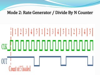
- 17. Mode 2: Rate Generator / Divide by N Counter When N is loaded as count after N pulses OUT goes low for only one clock cycle then, count N is reloaded OUT becomes high for N clock pulses The number of clock pulses between the two low pulses is equal to the count loaded Gate logic 0 no counting Gate logic 1 normal counting
- 18. Mode 2: Rate Generator / Divide By N Counter
- 20. Mode 3: SQUARE WAVE RATE GENERATOR 1. When count N loaded is even output remains HIGH for half the count and LOW for the rest half of the count 2. When count N loaded is odd output remains HIGH for (N+1)/2 and low for (N-1)/2. 3. Repeated operation gives square wave 4. Generates a continuous square-wave with G set to 1. 5. If count is even, 50% duty cycle otherwise OUT is high 1 cycle longer.
- 21. Mode 3: Square Wave Generator
- 22. After mode is set output goes high When count is loaded counting down starts on reaching terminal count output goes low for only one clock cycle, and then again output goes HIGH The above said low pulse can be used as a strobe for interfacing MP with peripherals When GATE is LOW counting is inhibited and count is latched If a new count is loaded while counting, previous counting stops and new counting started in next clock cycle Mode 4: Software triggered Strobe
- 24. 24
- 25. This mode generates a strobe in response to the rising edge at the trigger Mode is used to generate a delayed strobe in response to an externally generated signal Once mode is programmed and counter loaded, OUT goes HIGH Counter starts counting after the rising edge of the trigger (GATE) The OUTPUT goes LOW for one clock period, when the terminal count is reached Output will not go LOW until the counter content becomes zero after the rising edge of any trigger GATE is used as trigger input Mode 5: Hardware triggered Strobe
- 26. Mode 5: Hardware triggered Strobe
- 27. Read Operations There are three possible methods for reading the counters: 1. a simple read operation 2. the Counter Latch Command 3. the Read-Back Command 1. Simple read operation : The Counter which is selected with the A1, A0 inputs, the CLK input of the selected Counter must be inhibited by using either the GATE input or external logic. Otherwise, the count may be in the process of changing when it is read, giving an undefined result.
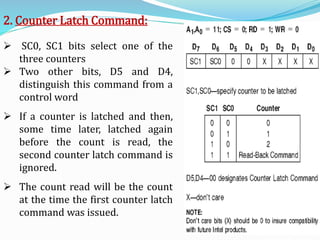
- 28. 2. Counter Latch Command: SC0, SC1 bits select one of the three counters Two other bits, D5 and D4, distinguish this command from a control word If a counter is latched and then, some time later, latched again before the count is read, the second counter latch command is ignored. The count read will be the count at the time the first counter latch command was issued.
- 29. 3. Read-back control command: The read-back control, word is used, when it is necessary for the contents of more than one counter to be read at a same time. Count : logic 0, select one of the Counter to be latched Status : logic 0, Status must be latched to be read status of a counter and is accessed by a read from that counter
- 30. Status register: •Shows the state of the output pin •Check the counter is in null state (0) or not •How the counter is programmed