
![SYSTEMATIC APPROACH TO BEHAVIORAL MODELING
CDNLIVE, MARCH 10, 2015
© 2015 XtremeEDA All Rights Reserved
PAGE 2
ABSTRACT
We present a systematic approach for creating accurate analog
and mixed-signal (AMS) behavioral models for system design and
verification. Our approach reduces the risk of system failure
resulting from model error, whether model error comes from
initial misunderstanding or miscommunication of design
revision. This paper, which accompanies a CDNLive presentation
of the same title is targeted toward model designers, but is
of interest to verification engineers, circuit designers, and
engineering managers.
Although our approach is platform-independent, we demonstrate
our procedure using the Cadence Design System. Virtuoso is the
starting point for generating models and test benches. We make
use of AMSDMV (Analog Mixed-Signal Design and Model
Validation) and we define interactive procedures for model
creation, validation, and maintenance based upon expected
behavior. This approach applies to any modeling language,
including Verilog or System Verilog using real number modeling
(RNM), Verilog-AMS (including WREAL), and Verilog-A. And for
models intended for UVM, Verilog, or Verilog-AMS simulation
platforms.
Between them, the authors have more than 40 years’ behavioral
modeling experience. This paper shares the approach they
developed first individually at various companies and then
collaboratively at XtremeEDA.
1. INTRODUCTION
1.1. INDUSTRY TRENDS AND OBSERVATIONS
As of 2015, System-on-Chip (SOC) size and complexity continues
to increase [1], because traditional economic drivers remain
in place such as reduced physical dimensions, extended battery
life, and lower price for end product. Analog and mixed signal
(AMS) content continue to be brought onboard the SOC despite
the difficulty for analog performance not to degrade as
geometry shrinks in advanced nodes. In fact,](https://image.slidesharecdn.com/51896166-ea24-455a-9cfc-bbb562db5d74-160616234251/85/A-Systematic-Approach-to-Creating-Behavioral-Models-white-paper-v1-0-2-320.jpg)
![SYSTEMATIC APPROACH TO BEHAVIORAL MODELING
CDNLIVE, MARCH 10, 2015
© 2015 XtremeEDA All Rights Reserved
PAGE 3
IBS reports that mixed signal accounts for over
85% of chip design starts in 2014, and that
percentage will rise, and hold steady at 85% in
the coming years [2]
The 2013 prediction [3] was that 130nm would continue to be
the most popular AMS technology node. Meanwhile, 65nm is now
considered mainstream [4], and the number of 28nm tape-outs
and designs in progress is increasing. As of 2013, analog
design problems at less than 28nm had yet to be solved [5].
The accepted solution is to use digital compensation and
calibration in analog building blocks.
Time to market remains all-important. This conflicts with the
requirement that verification quality must not degrade. The
conflict is resolved by simulator performance increasing.
Digital design and analog design follow fundamentally
different procedures. Each flow has unique requirements, tools
and skills. Thus the design teams are separated in outlook if
not geographically. The gap must be bridged to successfully
bring a mixed signal SOC to market. The interface between
analog and digital circuitry is a likely place for faults to
occur.
1.2. INDUSTRY CHALLENGES
Beyond the physical challenges of mixed-signal design in nano-
scale technology is the verification challenge of
manufacturing a large, complex SOC which is free of design
defects.
Behavioral models make high-level AMS verification possible.
The models must accurately portray the circuit they represent,
however, and this is yet another realm in which human error
can creep in.
There is no automated way to generate accurate, high-
performance models. It’s a matter of due diligence, combined
with a deliberate and systematic approach. Such an approach is
the topic of this paper. The authors combined their separate
approaches, each honed over decades of experience, into the
procedure we present.](https://image.slidesharecdn.com/51896166-ea24-455a-9cfc-bbb562db5d74-160616234251/85/A-Systematic-Approach-to-Creating-Behavioral-Models-white-paper-v1-0-3-320.jpg)


![SYSTEMATIC APPROACH TO BEHAVIORAL MODELING
CDNLIVE, MARCH 10, 2015
© 2015 XtremeEDA All Rights Reserved
PAGE 28
IEEE Lehigh Valley Chapter Solid-State Circuits Society
(SSCS), and Chair of IEEE Philadelphia Consultants Network
(CONET). Robert lives in Bethlehem, PA with his wife, Esther.
They are the parents of two adult children and grandparents of
a delightful one-year-old.
8.2. JOE MEDERO
Joe is a Principal Engineer at XtremeEDA Corporation. He
specializes in Modeling and Verification of Analog, Mixed-
Signal IC's and SOC's. His recent experiences include modeling
and verification of Serial Links (PMA, PHY's) and DDR I/O in
both Analog and Digital platforms. Joe obtained his BS in
Computer Engineering at the University of Puerto Rico at
Mayaguez and his MSEE from North Carolina State University. In
his first job he worked at IBM as a VLSI CAD Engineer where he
supported digital, gate-array, custom, semi-custom and analog
engineers in their designs and use and customization of the
tools. As an Analog Engineer at IBM he saw the need to verify
the system and started writing models for both the analog and
digital blocks. In 1998 he joined Cadence's Analog Mixed
Signal services group as an Analog Engineer working in
different projects that included Serial Links, Comparators,
ADC's, DAC's, etc. as required by the different customers and
most recently in the Cadence IP group. During his first year
he developed the first models that were used by the Services
group which allowed both the Analog Engineers as well as
digital engineers to test the individual blocks and the
system. Issues with inversions, power-supply and connectivity,
and timing where quickly found and addressed and led to many
first pass success stories at Cadence. His modeling and
verification experience at Cadence expanded into real number
modeling specifically with wreals which has been invaluable in
verifying Serial links especially the DFE algorithms used in
recovering the data.
9. REFERENCES
[1] M. Mota, "Debunking myths about analog IP at 28 nm," Planet Analog, 3 December 2012.
[Online]. Available: http://www.planetanalog.com/document.asp?doc_id=532472 [Accessed 23 February 2015]](https://image.slidesharecdn.com/51896166-ea24-455a-9cfc-bbb562db5d74-160616234251/85/A-Systematic-Approach-to-Creating-Behavioral-Models-white-paper-v1-0-28-320.jpg)
![SYSTEMATIC APPROACH TO BEHAVIORAL MODELING
CDNLIVE, MARCH 10, 2015
© 2015 XtremeEDA All Rights Reserved
PAGE 29
[2] Steve Carlson. "Five Reasons I'm Excited About Mixed-Signal Verification in 2015," Cadence
Design Systems, 3 December 2014. [Online]. Available:
http://community.cadence.com/cadence_blogs_8/b/ms/archive/2014/12/03/mixed-signal-design-verification-trends-
2015 [Accessed 23 February 2015]
[3] AnySilicon, "Semiconductor Technology Nodes – History, Trends and Forecast," AnySilicon, 7
June 2013. [Online]. Available: http://anysilicon.com/semiconductor-technology-nodes/ [Accessed 23 February
2015].
[4] M. Nizic, "How to Design Analog/Mixed Signal (AMS) at 28nm," Cadence Design Systems, 21
June 2011. [Online]. Available: http://community.cadence.com/cadence_blogs_8/b/ms/archive/2011/06/21/is-
anyone-designing-ams-at-28nm [Accessed 23 February 2015].
[5] L. Joselyn, "Analogue and mixed signal IP designers face challenges at 20nm,"
NewElectronics, 22 January 2013. [Online]. Available: http://www.newelectronics.co.uk/electronics-
technology/analogue-and-mixed-signal-ip-designers-face-challenges-at-20nm/47468/ [Accessed 23 February 2015].](https://image.slidesharecdn.com/51896166-ea24-455a-9cfc-bbb562db5d74-160616234251/85/A-Systematic-Approach-to-Creating-Behavioral-Models-white-paper-v1-0-29-320.jpg)
A Systematic Approach to Creating Behavioral Models (white paper) v1.0
- 1. www.xtreme-eda.com © 2015 XtremeEDA All Rights Reserved A Systematic Approach to Creating Behavioral Models CDNLive March 10, 2015 Robert O. Peruzzi, Jose Medero XtremeEDA Ottawa, ON, Canada [email protected], [email protected] Revision 1.0
- 2. SYSTEMATIC APPROACH TO BEHAVIORAL MODELING CDNLIVE, MARCH 10, 2015 © 2015 XtremeEDA All Rights Reserved PAGE 2 ABSTRACT We present a systematic approach for creating accurate analog and mixed-signal (AMS) behavioral models for system design and verification. Our approach reduces the risk of system failure resulting from model error, whether model error comes from initial misunderstanding or miscommunication of design revision. This paper, which accompanies a CDNLive presentation of the same title is targeted toward model designers, but is of interest to verification engineers, circuit designers, and engineering managers. Although our approach is platform-independent, we demonstrate our procedure using the Cadence Design System. Virtuoso is the starting point for generating models and test benches. We make use of AMSDMV (Analog Mixed-Signal Design and Model Validation) and we define interactive procedures for model creation, validation, and maintenance based upon expected behavior. This approach applies to any modeling language, including Verilog or System Verilog using real number modeling (RNM), Verilog-AMS (including WREAL), and Verilog-A. And for models intended for UVM, Verilog, or Verilog-AMS simulation platforms. Between them, the authors have more than 40 years’ behavioral modeling experience. This paper shares the approach they developed first individually at various companies and then collaboratively at XtremeEDA. 1. INTRODUCTION 1.1. INDUSTRY TRENDS AND OBSERVATIONS As of 2015, System-on-Chip (SOC) size and complexity continues to increase [1], because traditional economic drivers remain in place such as reduced physical dimensions, extended battery life, and lower price for end product. Analog and mixed signal (AMS) content continue to be brought onboard the SOC despite the difficulty for analog performance not to degrade as geometry shrinks in advanced nodes. In fact,
- 3. SYSTEMATIC APPROACH TO BEHAVIORAL MODELING CDNLIVE, MARCH 10, 2015 © 2015 XtremeEDA All Rights Reserved PAGE 3 IBS reports that mixed signal accounts for over 85% of chip design starts in 2014, and that percentage will rise, and hold steady at 85% in the coming years [2] The 2013 prediction [3] was that 130nm would continue to be the most popular AMS technology node. Meanwhile, 65nm is now considered mainstream [4], and the number of 28nm tape-outs and designs in progress is increasing. As of 2013, analog design problems at less than 28nm had yet to be solved [5]. The accepted solution is to use digital compensation and calibration in analog building blocks. Time to market remains all-important. This conflicts with the requirement that verification quality must not degrade. The conflict is resolved by simulator performance increasing. Digital design and analog design follow fundamentally different procedures. Each flow has unique requirements, tools and skills. Thus the design teams are separated in outlook if not geographically. The gap must be bridged to successfully bring a mixed signal SOC to market. The interface between analog and digital circuitry is a likely place for faults to occur. 1.2. INDUSTRY CHALLENGES Beyond the physical challenges of mixed-signal design in nano- scale technology is the verification challenge of manufacturing a large, complex SOC which is free of design defects. Behavioral models make high-level AMS verification possible. The models must accurately portray the circuit they represent, however, and this is yet another realm in which human error can creep in. There is no automated way to generate accurate, high- performance models. It’s a matter of due diligence, combined with a deliberate and systematic approach. Such an approach is the topic of this paper. The authors combined their separate approaches, each honed over decades of experience, into the procedure we present.
- 4. SYSTEMATIC APPROACH TO BEHAVIORAL MODELING CDNLIVE, MARCH 10, 2015 © 2015 XtremeEDA All Rights Reserved PAGE 4 2. BACKGROUND: BRIDGING THE ANALOG – DIGITAL SOC VERIFICATION GAP 2.1. DIGITAL VERIFICATION’S EVOLUTION INTO MIXED-SIGNAL VERIFICATION WHEN YOU GET TO THE BOTTOM, IT’S ALL ANALOG The transistors in a digital circuit are the same as the transistors in an analog circuit. But because the transistors of a digital circuit are constrained to settle into either cut-off or saturation mode we can simplify view of its behavior. By ignoring the relatively short transitions between cut-off and saturation modes we can ignore its electrical behavior and adopt a very simple behavioral model for a digital circuit. With this leap of faith as its basis, this became logic simulation. WITH DIGITAL CONSTRAINTS, LOGICAL RATHER THAN PHYSICAL SIMULATION IS POSSIBLE Once the concept of operating mode constraint was accepted, digital ICs could be designed and verified using logic simulation – without concern for analog realities. A methodology developed, evolved over the decades and became standardized into what is now SystemVerilog (SV) and the Universal Verification Methodology (UVM). Hallmarks of SV are constrained-random testing and object-orientation. Hallmarks of the UVM, an implementation of SV, are automation, and the awareness and measurement of verification coverage. ANALOG DOESN’T FIT LOGIC CONSTRAINT, BUT MAY BE FORCE-FITTED AT RISK All was well as long as there was no analog functionality. But as chips evolved into SOCs analog functionality began creeping into the design (because by integrating analog functionality, a lot of money could be made). This was okay as long as we could pretend it isn’t really analog. Some examples: A voltage regulator’s input from an off-chip power source could be considered a logic-1, its ground could be considered logic-0, and its output (which was traditionally ignored in logic simulation anyway) could also be a logic-1
- 5. SYSTEMATIC APPROACH TO BEHAVIORAL MODELING CDNLIVE, MARCH 10, 2015 © 2015 XtremeEDA All Rights Reserved PAGE 5 We could pretend a phase-locked-loop frequency synthesizer is just an ideal clock source We could ignore the entire analog front end up to and including the analog to digital converter (ADC) and treat the ADC output as the input source of digital stimulus These digital models representing analog circuits are oversimplified in that they cannot be used to verify all chip functions. If the model is to remain simple, and the circuit to appear digital then not all input behavior can be modeled. This leaves a gap in verification coverage, and allows design errors to go undetected. REAL NUMBER MODELING ENABLES THE FIT BETWEEN ANALOG AND LOGIC A more accurate representation of the circuit is needed, including a representation of analog signal flow and control. RNM is the answer. Two important principles of real number modeling allow event- driven simulation of analog circuitry. 1. Signal flow, not electrical networks. Signals may represent voltage or current – not both – so the physical nature of power, voltage and current cannot be modeled. This limits the type of circuits that can be modeled. For instance, a gain stage with high input impedance, and low output impedance driving into another high impedance input is a good RNM candidate. As a counter example resistors and capacitors joined in an RC network cannot be modeled individually using RNM. Instead, we group them into a subcircuit and create an RNM view of that subcircuit’s functionality. 2. Discrete-time samples of real numbers represent the analog signal. We use an imaginary clock to sample the signal at a rate much higher than the highest frequency of interest. Dynamic functions such as filters are modeled by difference equations rather than by differential equations as used in continuous-time models. The discrete-time and signal flow natures of RNM models allow their use in event-driven simulation without using an analog
- 6. SYSTEMATIC APPROACH TO BEHAVIORAL MODELING CDNLIVE, MARCH 10, 2015 © 2015 XtremeEDA All Rights Reserved PAGE 6 solver. Thus RNM makes it possible to verify an entire mixed- signal SOC from the top level using the UVM. 2.2. ANALOG VERIFICATION’S EVOLUTION INTO MIXED-SIGNAL VERIFICATION Originally, analog ICs were designed and verified without concern for digital sensibilities. After all, representing logic-1 as VDD, the power supply voltage and logic-0 as VSS is the more accurate representation, right? Well, yes, but... Conceptually, the complete verification of an arbitrarily large IC or SOC at the lowest-level device netlist might be possible, given unlimited time or computing power. Obviously that’s not practical. SOCs would never have evolved had we not taken the leap of faith to digital logic verification, which led to the UVM. Even all-analog circuits became unwieldy enough that subcircuit models became necessary. Thus, analog behavioral models came about, and evolved further into analog/mixed- signal (AMS) behavioral models. VERILOG-A (AND VHDL-A) MODELS ARE PHYSICALLY CONSERVATIVE AT PORTS Analog verification evolved through a separate path toward SOC verification. Analog behavioral models were the breakthrough allowing analog verification to evolve. Verilog-A was the first stage. Verilog-A is physically conservative, meaning that Kirchhoff’s voltage and current laws are obeyed. Device models (such as transistors, resistors, capacitors, and inductors) for Spectre and other SPICE-like simulators are also conservative. Verilog-A does not simulate digital logic. Models of standard logic functions obey Kirchhoff’s laws at their ports. Internal behavior may be represented by logic expressions or signal flow expressions, but the ports must be conservative. ANALOG/MIXED-SIGNAL SIMULATORS CONCURRENTLY RUN TWO ENGINES AMS simulators enable concurrent digital and analog simulation. They coordinate an analog simulation engine with an event-driven digital logic simulation engine. The analog simulation engine simulates netlists of basic lumped-parameter
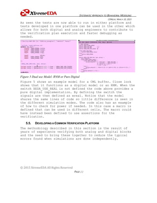
- 7. SYSTEMATIC APPROACH TO BEHAVIORAL MODELING CDNLIVE, MARCH 10, 2015 © 2015 XtremeEDA All Rights Reserved PAGE 7 devices and Verilog-A models. The digital simulation engine simulates netlists of Verilog models, which may be of individual logic gates, synthesizable RTL or non-synthesizable behavioral digital functions. The next step is the Verilog-AMS model, partitioned into analog and digital sections. When compiled and elaborated into a simulate-able database, the model’s behavior is apportioned between the digital and analog simulation engines. A certain amount of crossover between simulation engines takes place to allow truly mixed-signal operation. VERILOG-AMS (OR VHDL-AMS) It is Verilog-AMS models which make mixed-signal SOC verification possible with an AMS simulator at the top level. The drawback of AMS modeling is its use of an analog simulation engine – making it incompatible with SV and UVM. SystemVerilog-AMS and UVM-AMS may be on their way, but for now, it is RNM modeling with Verilog, VHDL or SystemVerilog that bridges the gap between analog and digital, and makes mixed signal use of UVM possible and attractive. 3. MODELING APPROACH Models are necessary, but it cannot be denied that a bad model is worse than no model at all. A model may be wrong because of initial misunderstanding or because the circuit has changed and the model has not been revised. There’s no completely automatic way to generate and update behavioral models, so we present a systematic approach which reduces the likelihood of modeling errors finding their way into design verification. 3.1. USE AUTOMATION WHEN POSSIBLE AND APPROPRIATE Schematic, symbol and model views need to be pin-identical. They must have identical pin names and order. This is automatically checked in the Cadence Virtuoso environment and in similar EDA environments. To automatically create the shell of a model which correctly matches its schematic, (or symbol) Open a schematic (or symbol) of the block to be modeled
- 8. SYSTEMATIC APPROACH TO BEHAVIORAL MODELING CDNLIVE, MARCH 10, 2015 © 2015 XtremeEDA All Rights Reserved PAGE 8 Automatically create the shell of the model, with I/O matching the schematic and symbol Make use of “Check and Save” to keep I/O in sync between schematic, symbol and model See Figure 1 Figure 1 Automatically Maintain Schematic, Symbol and Model I/O 3.2. COLLABORATE WITH CIRCUIT DESIGNER TO UNDERSTAND THE CIRCUIT STUDY THE SCHEMATIC Before you begin writing model code, get a complete grasp of the circuit’s behavior. Study the schematic. Write and sketch your own interpretation of the circuit. Jot down notes and questions. 3.3. INTERVIEW THE DESIGNER After studying the schematic, collaborate with the designer to understand the function of every aspect of the circuit. 3.4. DEVELOP THE CIRCUIT DESCRIPTION Create an accurate, complete, yet concise description of circuit functionality. Describe the actual circuit, that is,
- 9. SYSTEMATIC APPROACH TO BEHAVIORAL MODELING CDNLIVE, MARCH 10, 2015 © 2015 XtremeEDA All Rights Reserved PAGE 9 not just the model. Use whatever method best conveys the idea – a list of pins with description, equations, tables of characteristics versus input combinations, drawings. Comment the circuit description into the model file. Some text editors such as nedit have a rectangular drag-and-drop feature making it easy to create diagrams, tables and waveforms out of ASCII characters, as in Figure 2 Figure 2 Circuit Description as Comments within Model 3.5. CONFIRM THE CIRCUIT DESCRIPTION WITH THE DESIGNER The designer blesses the description. Neither party should take this lightly. It is a serious two-way commitment. The designer is obligated to inform the model owner regarding any change to pin-out or behavior. The model owner is obligated to keep the description up-to-date. Breaking either commitment endangers the integrity of the model and increases the risk of silicon failure. It is a matter of due diligence. There is no foolproof way to force compliance. A CAD-tool script (e.g. Skill in the case of Cadence EDA tools) may be written to create a sign-off form as a commented text on schematics and symbols. In this approach,
- 10. SYSTEMATIC APPROACH TO BEHAVIORAL MODELING CDNLIVE, MARCH 10, 2015 © 2015 XtremeEDA All Rights Reserved PAGE 10 executing “check-and-save” sends e-mail notices and causes indicators on the schematic and symbol to flash red until the model owner (and other interested people) sign off that they have approved the change. In practice this is only a reminder and sometimes an annoyance. It once again boils down to due diligence. 3.6. DECIDE WHICH BEHAVIORS TO INCLUDE IN THE MODEL Study the full-chip verification plan. Understand the role of the circuit to be modeled plays in each testcase. Get a feel for how much detail is required in the model. Interview the lead verification engineer to decide which behaviors of the circuit must be included in the model and which may be omitted. POSSIBLY OMIT CERTAIN BEHAVIORS FROM MODEL FIXED BANDWIDTH The fixed bandwidth of an amplifier may be well beyond the spectrum of interest for all test scenarios. If so, omitting bandwidth from the model eliminates the solving of a differential equation, and speeds up model execution. PROGRAMMABLE BANDWIDTH What if the bandwidth is digitally programmable? For the applicable testcases you may want to model that bandwidth. For others you may want to use assertions to verify the programmability path. ADAPTIVE BANDWIDTH What if the bandwidth is digitally controlled by an adaptation algorithm involving a digital state machine? Here again, that state machine may be more thoroughly verified using constrained random techniques than with analog signals. POWER SUPPLY SENSITIVITY Misrouting of power supplies is a typical source of error. More so when there are multiple power domains. An obvious
- 11. SYSTEMATIC APPROACH TO BEHAVIORAL MODELING CDNLIVE, MARCH 10, 2015 © 2015 XtremeEDA All Rights Reserved PAGE 11 verification is for each model to monitor and assert the acceptable power supply voltage range. Maybe, especially in the case of single power supply, you can speed up simulation by treating VDD as a logic signal, and each model monitoring and asserting that VDD is at logic-1 for operation. Standard logic gate models evolved without any sensitivity to power or ground. Nobody thought ahead to a multiple power domains, power switching to extend battery life etc. Some people took the approach of adding power sensitivity to their gate libraries. Others developed the concept of Common Power Format (CPF). As described elsewhere in this paper, CPF works so well that you may consider using it in your analog models. Kind of ironic that a solution for power-ignorance may work better than straightforward power-awareness. It’s worth considering, because it’s a net performance gain whenever you can maintain coverage while simplifying the job of the analog solver. EXAMPLE: DIFFERENT PLL MODELS FOR DIFFERENT TESTCASES
- 12. SYSTEMATIC APPROACH TO BEHAVIORAL MODELING CDNLIVE, MARCH 10, 2015 © 2015 XtremeEDA All Rights Reserved PAGE 12 EXAMPLE: DIFFERENT MODEL REPRESENTATIONS OF SETTLING TRANSIENTS Figure 3Realistic versus Simplified Transient Responses EXAMPLE: INCLUDING OR OMITTING ANALOG FRONT END
- 13. SYSTEMATIC APPROACH TO BEHAVIORAL MODELING CDNLIVE, MARCH 10, 2015 © 2015 XtremeEDA All Rights Reserved PAGE 13 Figure 4 Alternative Representations of Analog Front End 3.7. CONFIRM THE MODEL PLAN WITH THE DESIGNER AND VERIFICATION LEAD The lead verification engineer and designer bless the plan and it becomes part of the model description, commented within the model. It is another major commitment from all three parties to communicate any changes in plans. 3.8. WRITE THE MODEL Writing the code from the description is comparably easy, if you know the modeling languages. Writing model code is not easy if you don’t know how to do it. Take a course, read the books, take part in online forums, get experience. This paper is all about the approach, not the syntax. Here is a partial list of behavioral modeling languages. Model languages suitable for SV in UVM are indicated: Verilog-A o Electrical modeling techniques which conserve current and voltage laws for all ports. Electrical operations, mathematical or logical operations may AFE DSP CLKStimulus (Digital) AFE Pre-amp VGA CTF A/D DSP CLK Stimulus (Analog) A FE AFE
- 14. SYSTEMATIC APPROACH TO BEHAVIORAL MODELING CDNLIVE, MARCH 10, 2015 © 2015 XtremeEDA All Rights Reserved PAGE 14 be used internally to the model, but ports must be electrical. Can be more accurate but may execute more slowly compared to other model types. o Analog, and analog representation of digital o Runs on Spectre, SPICE and other device-level simulators o Runs on AMS simulators o Does not run on digital-only simulators Verilog-AMS o Electrical, wreal, or logic ports and wires o Electrical modeling techniques conserve current and voltage laws for analog signals, static biases, references, and power supplies o Real number modeling (RNM) with wreal ports and wires for analog signal flow o Logic ports and internal operations o Runs only on AMS simulators o Does not run on Spectre, SPICE or other device-level simulators o Does not run on digital-only simulators VHDL-A (Similar to Verilog-A) o Electrical modeling techniques which conserve current and voltage laws for all ports. Electrical operations, mathematical or logical operations may be used internally to the model, but ports must be electrical. Can be more accurate but may execute more slowly compared to other model types. o Analog, and analog representation of digital o Runs on Spectre, SPICE and other device-level simulators o Runs on AMS simulators o Does not run on digital-only simulators VHDL-AMS (Similar to Verilog-AMS) o Electrical, real, or logic ports and wires o Electrical modeling techniques conserve current and voltage laws for analog signals, static biases, references, and power supplies
- 15. SYSTEMATIC APPROACH TO BEHAVIORAL MODELING CDNLIVE, MARCH 10, 2015 © 2015 XtremeEDA All Rights Reserved PAGE 15 o Real number modeling (RNM) with real ports and wires for analog signal flow o Logic ports and internal operations o Runs only on AMS simulators o Does not run on Spectre, SPICE or other device-level simulators o Does not run on digital-only simulators Verilog (Good for RNM in UVM) o Logic. Only logic ports and wires o RNM with internal real variables and out-of-module references (OOMR) for analog signal flow o Runs on event driven digital-only simulators such as Incisive, VCS, ModelSim o Runs on AMS simulators o Does not run on Spectre, SPICE or other device-level simulators VHDL (Good for RNM in UVM) o Logic and real ports and wires o RNM with real ports and wires for analog signal flow o Runs on event driven digital-only simulators such as Incisive, VCS, ModelSim o Runs on AMS simulators o Does not run on Spectre, SPICE or other device-level simulators SystemVerilog (Good for RNM in UVM) o Logic and real ports and wires o RNM with real ports and wires for analog signal flow o Verification-centric with random-stimulus emphasis o Object-Oriented o Runs on event driven digital-only simulators such as Incisive, VCS, ModelSim o Runs on AMS simulators o Does not run on Spectre, SPICE or other device-level simulators SystemVerilog-AMS o Logic o Verification-centric with random-stimulus emphasis
- 16. SYSTEMATIC APPROACH TO BEHAVIORAL MODELING CDNLIVE, MARCH 10, 2015 © 2015 XtremeEDA All Rights Reserved PAGE 16 o Object-Oriented o Electrical modeling techniques which conserve current and voltage laws for analog signals and static biases, references and power supplies can be the most accurate but execute more slowly o RNM with real wires and ports for analog signal flow o Runs on AMS simulators o Does not run on Spectre, SPICE or other device-level simulators o Does not run on digital-only simulators 4. VALIDATING MODELS Every model must be validated. Validation is typically done on a testbench schematic separate from the full chip environment. It’s not always about matching model simulations to the schematic. For certain testcases you don’t even want a model to behave like the schematic. The main thing is, you validate that the model matches the agreed-upon plan. Validation answers two questions: 1. Does the model view match its plan? 2. Does the model respond to all input scenarios, including bad logic and illegal combinations? In the ideally best practice the model be validated by someone other than its author, but the analog designer shouldn't have to learn Verilog-AMS or even how to run the AMS simulator to do so. Here is an approach that is a workable compromise: 4.1. DOES THE MODEL VIEW MATCH ITS PLAN? 1. Model designer creates a testbench schematic which instantiates and connects symbols for the device under test (DUT) and a driver-monitor (DMON) 2. Circuit and model designers collaborate to describe analog and digital stimulus 3. Model designer creates DMON stimulus, simulates the schematic, and simulates the model 4. Debug until the model simulation is correct. That is, so that it matches either the schematic simulation or
- 17. SYSTEMATIC APPROACH TO BEHAVIORAL MODELING CDNLIVE, MARCH 10, 2015 © 2015 XtremeEDA All Rights Reserved PAGE 17 conforms to the planned response, where different from the physical circuit 5. Model designer delivers a turnkey simulation scenario to the circuit designer. This could be a Cadence “analog artist” state for instance, which is comfortable for the circuit designer to execute and examine 6. Circuit designer reruns the simulation in a familiar environment, and “blesses” the model and its stimulus and response 4.2. DOES THE MODEL RESPOND TO ALL INPUT SCENARIOS, INCLUDING BAD LOGIC AND ILLEGAL COMBINATIONS? In the course of full chip testcases the model may receive unexpected input. When this happens it is very important that the model not cause the simulator to crash. Worse than that would be if the model were to ignore the faulty input and go on as if all is well. For example, passing signals when there’s no power supply, or when the power-down input is in the unknown state. Unfortunately there are infinite combinations of no-good input controls and analog waveforms. So the model designer does his best to come up with a good enough set to try out all the model's fault detecting code (i.e. assertions). The design engineer and lead verification engineer may critique and request other input sequences. This part of validation is very important and tends to reduce the number of problems occurring in full chip simulation. It is based on experience and intuition. 1. Use constrained random approach where possible 2. Include out-of-range analog 3. Include illegal combinations of logic 4. Include unknown ‘x’ states The point is to ensure the model doesn’t “pretend” everything is okay, or hang the simulator when something goes wrong. 5. MODELS AND APPLICATIONS Different platforms require different levels of models to reach the verification goals of the system.
- 18. SYSTEMATIC APPROACH TO BEHAVIORAL MODELING CDNLIVE, MARCH 10, 2015 © 2015 XtremeEDA All Rights Reserved PAGE 18 Analog requirements traditionally have been about meeting the specification performance parameters while taking into account system parasitics and error sources to make sure operation of individual circuits and the full system are met across corners and statistical variations. Digital design was traditionally verified based on the use- model understanding of the design and verification teams. The verification effort was easily accomplished by a series of tests that verified different paths of the design (directed tests). With increased complexity and a higher user pool this use-model was proven to be limited and new testing methods were developed. From constrained-random, OVM, UVM, etc. test coverage has improved dramatically to predict different use- model scenarios resulting in higher verification success. 5.1. ANALOG VERIFICATION Pure Analog test benches are setup quickly by using library components that allows the engineer to set voltages, currents, resistances, etc. that drive and/or load the DUT. Complex stimulus blocks are modeled using an AHDL language such as VerilogA. With higher complexity and digital integration mixed-signal verification tools may be required. Many Analog engineers avoid this due to issues with interface elements (or connect modules) and the extra effort to setup configuration files and correct stop views. Digital blocks are then, many times, modeled using VerilogA. This provides a very successful analog verification methodology but obviously has issues if the digital block and VerilogA model do not match. ANALOG MIXED-SIGNAL SIMULATIONS Analog Mixed-Signal (AMS) Engineers are capable of bridging this gap in verification. Most of these engineers understand the complexity of analog circuits and have a solid background with digital RTL, behavioral and gate level circuits. Many simulations with Big-A and Little-D (mostly Analog with minimum digital blocks) can be fully verified with this type of platform. By using fast simulators such as APS-AMS,
- 19. SYSTEMATIC APPROACH TO BEHAVIORAL MODELING CDNLIVE, MARCH 10, 2015 © 2015 XtremeEDA All Rights Reserved PAGE 19 Ultrasim-AMS, Spectre XPS MS and setting the proper simulation precision for each block the system can be simulated quickly and precisely. Timing interfaces, calibration circuits, etc. could be covered with a limited set of tests that checks the important interface components and system performance parameters. The predictability of how the system is used allows for this type of verification to be sufficient. DIGITAL SIMULATIONS WITH AMS MODELS With advances in technology and smaller feature sizes more integration is available in an IC. Full SOC’s are now integrated with different IP’s including Analog IP. Creating tests that cover the use-space of the IP is now a daunting task that makes it very difficult to be covered in a slow simulation environment. SOC simulations typically run for microseconds, milliseconds and higher while analog simulation is limited due to the required time and resources. In such a system the Analog and Mixed-Signal verification methods mentioned previously still applies but it is also necessary to add another level of verification that can be used by the SOC integration and verification teams to make sure the system works in multiple use-model scenarios and in reasonable time. For small SOC’s the Analog can be modeled using mixed-signal languages, such as Verilog-AMS or VHDL-AMS, and integrated into the digital verification platform. This is much slower than a digital only simulation, therefore, the number of simulations used in this scenario should be limited to a set of tests that provide enough code and functional coverage for the system. 5.2. DIGITAL VERIFICATION For large SOC’s UVM allows highly complex systems to be verified due to the comprehensive testing included in the methodology. This includes integration of Analog IP as part of the SOC and verification plan.
- 20. SYSTEMATIC APPROACH TO BEHAVIORAL MODELING CDNLIVE, MARCH 10, 2015 © 2015 XtremeEDA All Rights Reserved PAGE 20 To test the analog, SOC design and verification teams may develop a model of the analog system based on the specifications and its description of the analog subsystem. Digital engineer’s knowledge of analog systems may be limited so the model may just be a code-coverage model to make sure signals are arriving at its destination. It is then the Analog Engineer’s responsibility to verify the block under all the different conditions. Many issues have been found with this type of verification approach which results in endless hours of root-cause analysis. Typical issues with this approach include specifications that are not up to date, uncommunicated analog block changes, misunderstanding of timing constraints or requirements, polarity changes, hierarchical differences in the model vs actual circuit, etc. From a digital verification perspective the verification metrics may be meeting the intended goals but is not capable of capturing all the issues mentioned above. From the Analog side all the required simulations have been completed and determined to be functional. As mentioned previously then it is of essence to develop models and a methodology that can accomplish the full verification of the system and make sure that the integration of analog and digital blocks represents the actual system being built. 5.3. POWER AWARE VERIFICATION Due to Green initiatives, mobile battery life concerns, multi- power supply systems, etc. designs need to be Power Aware to meet the lower power dissipation requirements of newer systems. A digital power-state-machine is in control of these and needs access to all power plains or islands in the SOC including those in the analog domain(s). Analog Engineers will simulate their blocks and subsystems to verify the operation of the block and measure current requirement of the system for the different power states. However, as the analog subsystem becomes more complicated the
- 21. SYSTEMATIC APPROACH TO BEHAVIORAL MODELING CDNLIVE, MARCH 10, 2015 © 2015 XtremeEDA All Rights Reserved PAGE 21 number of tests become unmanageable and the required simulation times makes this inefficient. There are other issues that may arise in an analog only simulation environment. Has the design team taking into account the in-rush current from powering up/down different circuits? What about using the proper isolation cells. What are the state retention requirements and initial system setup issues? Is the reset-state dependent on analog and digital states that are in a feedback loop that may keep the system in an unknown state when parts are built? These are issues that are not easy to capture in an Analog only test environment. The mixed-signal models may help but are too slow and complicated for the SOC team to use. Again, the need then arises for models that can capture the analog environment, including power states, to help speed up the analog verification and at the same time be able to run these in a digital platform where comprehensive tests can run to quantify the operation of the different power states of the system. 5.4. REAL NUMBER MODEL VERIFICATION Real Number Models provide a solution to the increased verification complexity problem. Implementation of this can be done with Wreal, System Verilog Real, etc. The advantage of this type of model is the increased performance in Analog simulation platforms and how well it fits to support digital verification methods such as UVM. In the Analog platform it can easily be combined with digital blocks (RTL or gates), AMS models and schematics or extracted views as necessary. By partitioning the design properly highly complex simulations can be completed to verify the system. Analog Engineers are using their familiar verification platform and are able to measure performance parameters quickly. The same model is used in a digital platform and issues in the digital side is quickly fixed by the digital team. Full functional and digital coverage is then possible on the system.
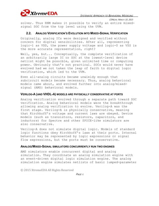
- 22. SYSTEMATIC APPROACH TO BEHAVIORAL MODELING CDNLIVE, MARCH 10, 2015 © 2015 XtremeEDA All Rights Reserved PAGE 22 As seen the tests are now able to run in either platform and tests developed in one platform can be used in the other which allows for both digital and analog engineers to contribute to the verification plan execution and faster debugging as needed. Figure 5 Dual use Model: RNM or Pure Digital Figure 5 shows an example model for a CML buffer. Close look shows that it functions as a digital model or an RNM. When the switch XEDA_USE_REAL is not defined the code above provides a pure digital implementation. By defining the switch the signals are then defined as wreal. Notice that the model shares the same lines of code so little difference is seen in the different simulation modes. The code also has an example of how to check for power if needed. In this case a macro is defined that can be used in different cells. The macro could have instead been defined to use assertions for the verification. 5.5. DEVELOPING A COMMON VERIFICATION PLATFORM The methodology described in this section is the result of years of experience verifying both analog and digital blocks and the need to bring these together to reduce the typical errors found when simulations are done independently.
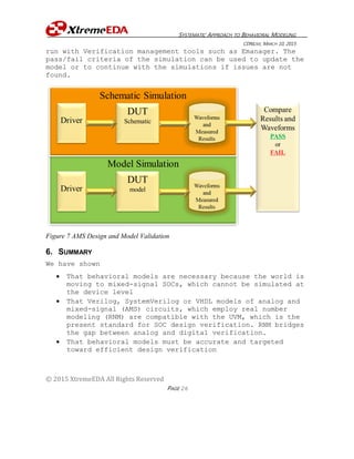
- 23. SYSTEMATIC APPROACH TO BEHAVIORAL MODELING CDNLIVE, MARCH 10, 2015 © 2015 XtremeEDA All Rights Reserved PAGE 23 Figure 6 Common Verification Platform As seen in Figure 6 both the digital verification and analog verification platforms are being used. However, the top level verification test bench is common for both environments. Key to the success of the methodology is allowing the digital and analog engineers to work in their familiar verification platforms. Tests now can be run in either/both environments to meet the verification goals required for each. Issues found in one platform can be investigated in the other. This is especially important to allow digital engineers to continue their work if issues are found in the analog side. From an analog perspective miscommunication issues are now limited as the analog team has full access to the digital RTL and/or gates and can determine if the system is performing and algorithms are converging as expected.
- 24. SYSTEMATIC APPROACH TO BEHAVIORAL MODELING CDNLIVE, MARCH 10, 2015 © 2015 XtremeEDA All Rights Reserved PAGE 24 By using RNM the verification is quickly run and issues can be investigated fully. If the need arises the Analog domain can change some of the views to more detailed models or actual schematics/extracted views. The integration of mixed signal verification into Spice type simulators such as Spectre-AMS, APS-AMS, Ultrasim-AMS, Spectre XPS MS, etc. allows the same test bench to be used with different views by just changing the configuration file in question. With AMS enabled configuration files the analog and digital simulation precision of individual blocks can be selected to allow for very efficient simulations. USING DIGITAL MODELS IN THE ANALOG ENVIRONMENT So now that we have an environment in which tests can be shared how do I know that I am using the latest digital RTL/gates and the latest Analog models? In the past the digital RTL was read into the Analog Virtuoso environment and the Mixed-signal verification team was able to run simulations with the Verilog as its own block with symbol and behavioral or functional (gates). An issue with this is that the digital may be changing and there is no guarantee that what is in the Analog libraries matches the digital libraries. To fix this AMS will allow you to compile the code into an open source library format. This worked but caused too long of a cycle due to possible multiple library compilations including foundry or vendor digital libraries. Instead of using this approach mixed-signal verification in an Analog platform has migrated to having a “stopping view” in the Analog environment. When the netlister finds this view it treats the circuit as a block box and expects that the needed model will be provided at simulation time. It is then the responsibility of the verification person to provide a manifest file that points to the location of the actual model or schematic for the block. Digital designers and verification teams should have a revision control methodology that ensures the latest digital
- 25. SYSTEMATIC APPROACH TO BEHAVIORAL MODELING CDNLIVE, MARCH 10, 2015 © 2015 XtremeEDA All Rights Reserved PAGE 25 code and tests are in use by providing scripts that update individual member work areas, set proper environment variables and provides manifest files that points to the latest code needed for simulations. Analog verification is then run after creating/updating the work area and pointing to the manifest files in the directory structure. Environment variables should be defined as full paths instead of relative paths (as is customary in digital simulations) since the analog simulations are not running directly in the simulation directory structure setup for digital verification. By having a revision control area for analog simulations and updating the area as needed the Analog team is guaranteed to be running with the latest code. If the need arises the team can use a different branch to test previous releases or to test new concepts without affecting the effort of the rest of the team. USING ANALOG MODELS IN THE DIGITAL ENVIRONMENT For digital verification to be successful the Analog models also should be under revision control in the digital environment. This is critical and may cause concerns to the Analog team as they no longer have direct access to the code. However, by using AMS in debug mode they have access to waveform tools such as simvision that can trace signals and display the model of the block if necessary. Even after adding the Analog Models to the revision controlled digital verification directory structure there is the question of the validity of stored models. How do we know that the checked-in models match the corresponding analog circuits? This was discussed in the Validating Models section. When Analog changes are done it is recommended that the Analog team re-run the simulations to make sure the models still match. In reality due to the increasing load and diminish time required to complete circuits this part is normally neglected. Therefore, a tool such as AMSDMV is then necessary. After the initial setup, AMSDMV allows the model validation simulations to be run with a set of regression scripts that can also be
- 26. SYSTEMATIC APPROACH TO BEHAVIORAL MODELING CDNLIVE, MARCH 10, 2015 © 2015 XtremeEDA All Rights Reserved PAGE 26 run with Verification management tools such as Emanager. The pass/fail criteria of the simulation can be used to update the model or to continue with the simulations if issues are not found. Figure 7 AMS Design and Model Validation 6. SUMMARY We have shown That behavioral models are necessary because the world is moving to mixed-signal SOCs, which cannot be simulated at the device level That Verilog, SystemVerilog or VHDL models of analog and mixed-signal (AMS) circuits, which employ real number modeling (RNM) are compatible with the UVM, which is the present standard for SOC design verification. RNM bridges the gap between analog and digital verification. That behavioral models must be accurate and targeted toward efficient design verification
- 27. SYSTEMATIC APPROACH TO BEHAVIORAL MODELING CDNLIVE, MARCH 10, 2015 © 2015 XtremeEDA All Rights Reserved PAGE 27 That there is no totally automatic way to create behavioral models, but that it is a collaborative effort between the circuit designer, the verification lead and the model writer A step-by-step procedure for planning, writing, validating and maintaining behavioral models That it is the collaborative nature of the procedure that increases the likelihood of error free models, and error free silicon 7. ACKNOWLEDGEMENT The authors thank Cadence Design Systems for allowing them to present their talk and this white paper at the March, 2015 CDNLive conference. Special thanks for the use of Cadence EDA tools for preparing our presentations. We also thank our XtremeEDA for sponsoring us, generously allowing us time for preparation and for our travel and accommodations for the conference. 8. AUTHOR BIOS 8.1. ROBERT PERUZZI Robert is a Principal Engineer at XtremeEDA Corporation. He specializes in behavioral modeling and verification of Analog, RF, and Mixed-Signal IC and SOC Designs, using Verilog (with Real Number Modeling), Verilog-AMS and Verilog-A. He moved to Allentown, Pennsylvania in 1990 to work as an ATE test developer for AT&T Bell Labs, where he took advantage of their study plan for continuing education. He earned his Ph. D. in 2005, after what seemed like an eternity of part time study. He stayed on as that company evolved into Lucent, Agere, LSI and Infineon. As opportunities arose he crossed between departments, working in analog and mixed signal design. Along the way he picked up expertise in Verilog-AMS, VHDL-AMS, Simulink and other design and verification skills, which have turned into his engineering passion. He was an independent consultant as R. Peruzzi Consulting, Inc., from 2009 to 2014 when he joined XtremeEDA. Robert is the founder, and Chair of
- 28. SYSTEMATIC APPROACH TO BEHAVIORAL MODELING CDNLIVE, MARCH 10, 2015 © 2015 XtremeEDA All Rights Reserved PAGE 28 IEEE Lehigh Valley Chapter Solid-State Circuits Society (SSCS), and Chair of IEEE Philadelphia Consultants Network (CONET). Robert lives in Bethlehem, PA with his wife, Esther. They are the parents of two adult children and grandparents of a delightful one-year-old. 8.2. JOE MEDERO Joe is a Principal Engineer at XtremeEDA Corporation. He specializes in Modeling and Verification of Analog, Mixed- Signal IC's and SOC's. His recent experiences include modeling and verification of Serial Links (PMA, PHY's) and DDR I/O in both Analog and Digital platforms. Joe obtained his BS in Computer Engineering at the University of Puerto Rico at Mayaguez and his MSEE from North Carolina State University. In his first job he worked at IBM as a VLSI CAD Engineer where he supported digital, gate-array, custom, semi-custom and analog engineers in their designs and use and customization of the tools. As an Analog Engineer at IBM he saw the need to verify the system and started writing models for both the analog and digital blocks. In 1998 he joined Cadence's Analog Mixed Signal services group as an Analog Engineer working in different projects that included Serial Links, Comparators, ADC's, DAC's, etc. as required by the different customers and most recently in the Cadence IP group. During his first year he developed the first models that were used by the Services group which allowed both the Analog Engineers as well as digital engineers to test the individual blocks and the system. Issues with inversions, power-supply and connectivity, and timing where quickly found and addressed and led to many first pass success stories at Cadence. His modeling and verification experience at Cadence expanded into real number modeling specifically with wreals which has been invaluable in verifying Serial links especially the DFE algorithms used in recovering the data. 9. REFERENCES [1] M. Mota, "Debunking myths about analog IP at 28 nm," Planet Analog, 3 December 2012. [Online]. Available: http://www.planetanalog.com/document.asp?doc_id=532472 [Accessed 23 February 2015]
- 29. SYSTEMATIC APPROACH TO BEHAVIORAL MODELING CDNLIVE, MARCH 10, 2015 © 2015 XtremeEDA All Rights Reserved PAGE 29 [2] Steve Carlson. "Five Reasons I'm Excited About Mixed-Signal Verification in 2015," Cadence Design Systems, 3 December 2014. [Online]. Available: http://community.cadence.com/cadence_blogs_8/b/ms/archive/2014/12/03/mixed-signal-design-verification-trends- 2015 [Accessed 23 February 2015] [3] AnySilicon, "Semiconductor Technology Nodes – History, Trends and Forecast," AnySilicon, 7 June 2013. [Online]. Available: http://anysilicon.com/semiconductor-technology-nodes/ [Accessed 23 February 2015]. [4] M. Nizic, "How to Design Analog/Mixed Signal (AMS) at 28nm," Cadence Design Systems, 21 June 2011. [Online]. Available: http://community.cadence.com/cadence_blogs_8/b/ms/archive/2011/06/21/is- anyone-designing-ams-at-28nm [Accessed 23 February 2015]. [5] L. Joselyn, "Analogue and mixed signal IP designers face challenges at 20nm," NewElectronics, 22 January 2013. [Online]. Available: http://www.newelectronics.co.uk/electronics- technology/analogue-and-mixed-signal-ip-designers-face-challenges-at-20nm/47468/ [Accessed 23 February 2015].