SlideShare a Scribd company logo
4
Most read
7
Most read
14
Most read
LAYOUT EXTRACTION
AGENDA
• Digital Design Flow
• Basics of Layout
• About Layout Extractor
• Tools used
• Steps to Extract layout
5-Jul-14 Medha.chhillar@gmail.com 2
Digital Design Flow
5-Jul-14 Medha.chhillar@gmail.com 3
Design Analysis
Design Specification
Synthesis
Design Implementation using HDL
Simulation
Timing Analysis
Place & Route
Extraction
Verification
Verilog/
VHDL
Library
Std., Cell.
Library
Look up
Table for
timing
Tech file
For layout
values
Tech file
For RC
Parasite
extraction
Basics of Layout
• Layout can be very time consuming
– Design gates to fit together nicely
– Build a library of standard cells
– Must follow a technology rule
• Standard cell design methodology
– VDD and GND should abut (standard height)
– Adjacent gates should satisfy design rules
– nMOS at bottom and pMOS at top
– All gates include well and substrate contacts
5-Jul-14 Medha.chhillar@gmail.com 4
What Are Layout Extractors??
• Once the layout is made, there always is parasitic
capacitances and resistances associated with the
design.
• This is because of the compact layouts to make the
chips smaller. More you make compact layout more
will it introduce these parasitic components.
• These interferes in the functioning and performance of
the circuit in terms of timing, speed and power
consumption.
5-Jul-14 Medha.chhillar@gmail.com 5
Contd…
• Examine the inter-relationship of mask layers
to infer the existence of transistors and other
components
• Related to Design Rule Checkers
– Design-rule Verification
• Some form of layout extraction is usually done
to create data for back annotation
5-Jul-14 Medha.chhillar@gmail.com 6
Tools used for Extraction
• FastCap, FastHenry
• Star-RCXT
• QRC
• Calibre xACT3D
etc…
5-Jul-14 Medha.chhillar@gmail.com 7
Steps to Extract a Layout
• Create Layout Cellview
• Design Rule Checking
• Layout Parameter Extraction
• Layout vs. Schematic Comparison
5-Jul-14
Courtesy:http://www.egr.msu.edu/classes/ece410/mason/files/TutorialB.pdf
8
Step1: Create Layout Cellview
From the schematic, we can draw the layout cellview
From the Library Manager window, Select File => New => Cellview
(Virtuoso is the main layout editor of Cadence design tools)
5-Jul-14 Medha.chhillar@gmail.com 9
Step2:Design Rule Checking
• After you have finished your layout, an automatic program will check
each and every polygon in your design against these design rules
and report violations. This process is called Design Rule Checking
(DRC) and MUST be done for every layout to ensure it will function
properly when fabricated.
• After the DRC is complete, the bottom line in the CIW(Command
Interpreter Window) will show “# Total errors found”
• The DRC will be successful when you see the results saying “0 Total
errors found”
5-Jul-14 Medha.chhillar@gmail.com 10
Step3: Layout Parameter
Extraction
• mask layout contains only physical data
• Extraction process identifies the devices from the layout and
generates a SPICE-like netlist and other files necessary to complete
the design process
• In the Virtuoso Layout Editing window select Verify => Extract
5-Jul-14 Medha.chhillar@gmail.com 11
Extracted Layout
Before After
5-Jul-14 Medha.chhillar@gmail.com 12
Conclusion
5-Jul-14 Medha.chhillar@gmail.com 13
Data Preparation
Draw Schematic
(Virtuoso)
Logic Simulation
(Verilog-XL)
Pre-layout Simulation
(Spectre)
Layout
(Virtuoso)
Design Rule Check
(Calibre)
Layout Versus
Schematic Check
(Calibre)
Extraction
(Calibre)
Post layout simulation
(HSPICE)
THANK YOU
5-Jul-14 Medha.chhillar@gmail.com 14

More Related Content

What's hot (20)

PPTX
2Overview of Primetime.pptx
ShivangPanara
 
PPTX
12 low power techniques
Ramakrishna Kittu
 
PDF
Clock Tree Timing 101
Silicon Labs
 
PDF
Synchronous and asynchronous reset
Nallapati Anindra
 
PPTX
CPLD & FPGA Architectures and applictionsplications.pptx
Dr.YNM
 
PDF
Vlsi design-styles
Praveen kumar Deverkonda
 
PPTX
System partitioning in VLSI and its considerations
Subash John
 
PPTX
ASIC DESIGN FLOW
Purvi Medawala
 
PDF
Chapter1.slides
Avinash Pillai
 
PPTX
Vlsi physical design automation on partitioning
Sushil Kundu
 
PDF
Physical design
Manjunath hosmani
 
PDF
Presentation systemc
SUBRAHMANYA S
 
PPTX
Define Width and Height of Core and Die (http://www.vlsisystemdesign.com/PD-F...
VLSI SYSTEM Design
 
PPT
Applications of ATPG
Ushaswini Chowdary
 
DOCX
Power Reduction Techniques
Rajesh M
 
PDF
2019 5 testing and verification of vlsi design_fault_modeling
Usha Mehta
 
PDF
Basic of AI Accelerator Design using Verilog HDL
Joohan KIM
 
PDF
Synchronous and asynchronous clock
Nallapati Anindra
 
PPTX
Placement in VLSI Design
Team-VLSI-ITMU
 
2Overview of Primetime.pptx
ShivangPanara
 
12 low power techniques
Ramakrishna Kittu
 
Clock Tree Timing 101
Silicon Labs
 
Synchronous and asynchronous reset
Nallapati Anindra
 
CPLD & FPGA Architectures and applictionsplications.pptx
Dr.YNM
 
Vlsi design-styles
Praveen kumar Deverkonda
 
System partitioning in VLSI and its considerations
Subash John
 
ASIC DESIGN FLOW
Purvi Medawala
 
Chapter1.slides
Avinash Pillai
 
Vlsi physical design automation on partitioning
Sushil Kundu
 
Physical design
Manjunath hosmani
 
Presentation systemc
SUBRAHMANYA S
 
Define Width and Height of Core and Die (http://www.vlsisystemdesign.com/PD-F...
VLSI SYSTEM Design
 
Applications of ATPG
Ushaswini Chowdary
 
Power Reduction Techniques
Rajesh M
 
2019 5 testing and verification of vlsi design_fault_modeling
Usha Mehta
 
Basic of AI Accelerator Design using Verilog HDL
Joohan KIM
 
Synchronous and asynchronous clock
Nallapati Anindra
 
Placement in VLSI Design
Team-VLSI-ITMU
 

Viewers also liked (13)

PPTX
Reduced ordered binary decision diagram
Team-VLSI-ITMU
 
PPTX
scripting in Python
Team-VLSI-ITMU
 
PPTX
RTX Kernal
Team-VLSI-ITMU
 
PPT
Computer Aided Design: Global Routing
Team-VLSI-ITMU
 
PPTX
CAD: Floorplanning
Team-VLSI-ITMU
 
PPTX
Computer Aided Design: Layout Compaction
Team-VLSI-ITMU
 
PPTX
CAD: introduction to floorplanning
Team-VLSI-ITMU
 
PPTX
Ch 6 randomization
Team-VLSI-ITMU
 
PPT
CNTFET
Team-VLSI-ITMU
 
PPT
VLSI routing
Naveen Kumar
 
PPTX
Nmos design using synopsys TCAD tool
Team-VLSI-ITMU
 
PPTX
twin well cmos fabrication steps using Synopsys TCAD
Team-VLSI-ITMU
 
PDF
VLSI-Physical Design- Tool Terminalogy
Murali Rai
 
Reduced ordered binary decision diagram
Team-VLSI-ITMU
 
scripting in Python
Team-VLSI-ITMU
 
RTX Kernal
Team-VLSI-ITMU
 
Computer Aided Design: Global Routing
Team-VLSI-ITMU
 
CAD: Floorplanning
Team-VLSI-ITMU
 
Computer Aided Design: Layout Compaction
Team-VLSI-ITMU
 
CAD: introduction to floorplanning
Team-VLSI-ITMU
 
Ch 6 randomization
Team-VLSI-ITMU
 
VLSI routing
Naveen Kumar
 
Nmos design using synopsys TCAD tool
Team-VLSI-ITMU
 
twin well cmos fabrication steps using Synopsys TCAD
Team-VLSI-ITMU
 
VLSI-Physical Design- Tool Terminalogy
Murali Rai
 
Ad

Similar to CAD: Layout Extraction (20)

PDF
Making of an Application Specific Integrated Circuit
SWINDONSilicon
 
PPT
B tech Projects,Final Year Projects,Engineering Projects
Technogroovy
 
PPTX
Sdlc
Kunal Pandhram
 
PPTX
System design techniques and networks
RAMPRAKASHT1
 
PPTX
ASIC design verification
Gireesh Kallihal
 
PPTX
The art of architecture
ADDQ
 
PPT
Unit 1 INTRODUCTION (COMPUTER AIDED DESIGN AND MANUFACTURING )
ravis205084
 
PPT
Processor Design Flow for architecture design
Varsha506533
 
PDF
AI Assisted Digital System Design Lecture 1
XeeshaCase
 
PPTX
Ece engineering embedded ppt -unit 2.pptx
ThalaThaya20
 
PDF
Digital VLSI Design : Introduction
Usha Mehta
 
PDF
SKEL 4273 CAD with HDL Topic 1
alhadi81
 
PPT
ASIC design Flow (Digital Design)
Sudhanshu Janwadkar
 
PPTX
DFA, Coding, CAPP engineering industrial .ppt
BishoyLabib7
 
PPT
Session2.pptx.ppt
AbdugafforAbduganiye
 
PPT
SDLC.PPT
SravyaPreethi1
 
PPT
SDLC.ppt
SnehaBarua5
 
PPT
Session2.ppt
DrJanarthananP
 
PPT
presentation ofSoftware Development Life Cycle (SDLC)
EveryThing68
 
Making of an Application Specific Integrated Circuit
SWINDONSilicon
 
B tech Projects,Final Year Projects,Engineering Projects
Technogroovy
 
System design techniques and networks
RAMPRAKASHT1
 
ASIC design verification
Gireesh Kallihal
 
The art of architecture
ADDQ
 
Unit 1 INTRODUCTION (COMPUTER AIDED DESIGN AND MANUFACTURING )
ravis205084
 
Processor Design Flow for architecture design
Varsha506533
 
AI Assisted Digital System Design Lecture 1
XeeshaCase
 
Ece engineering embedded ppt -unit 2.pptx
ThalaThaya20
 
Digital VLSI Design : Introduction
Usha Mehta
 
SKEL 4273 CAD with HDL Topic 1
alhadi81
 
ASIC design Flow (Digital Design)
Sudhanshu Janwadkar
 
DFA, Coding, CAPP engineering industrial .ppt
BishoyLabib7
 
Session2.pptx.ppt
AbdugafforAbduganiye
 
SDLC.PPT
SravyaPreethi1
 
SDLC.ppt
SnehaBarua5
 
Session2.ppt
DrJanarthananP
 
presentation ofSoftware Development Life Cycle (SDLC)
EveryThing68
 
Ad

More from Team-VLSI-ITMU (7)

PPTX
Intermediate Fabrics
Team-VLSI-ITMU
 
PDF
Linux Basics
Team-VLSI-ITMU
 
PPT
floor planning
Team-VLSI-ITMU
 
PDF
Cmos inverter design using tanner 180nm technology
Team-VLSI-ITMU
 
PPTX
SRAM- Ultra low voltage operation
Team-VLSI-ITMU
 
PDF
All opam assignment2_main
Team-VLSI-ITMU
 
PPT
MOSFET Small signal model
Team-VLSI-ITMU
 
Intermediate Fabrics
Team-VLSI-ITMU
 
Linux Basics
Team-VLSI-ITMU
 
floor planning
Team-VLSI-ITMU
 
Cmos inverter design using tanner 180nm technology
Team-VLSI-ITMU
 
SRAM- Ultra low voltage operation
Team-VLSI-ITMU
 
All opam assignment2_main
Team-VLSI-ITMU
 
MOSFET Small signal model
Team-VLSI-ITMU
 

Recently uploaded (20)

PDF
SG1-ALM-MS-EL-30-0008 (00) MS - Isolators and disconnecting switches.pdf
djiceramil
 
PPTX
sunil mishra pptmmmmmmmmmmmmmmmmmmmmmmmmm
singhamit111
 
PDF
settlement FOR FOUNDATION ENGINEERS.pdf
Endalkazene
 
PDF
4 Tier Teamcenter Installation part1.pdf
VnyKumar1
 
PDF
Zero Carbon Building Performance standard
BassemOsman1
 
PDF
All chapters of Strength of materials.ppt
girmabiniyam1234
 
PDF
67243-Cooling and Heating & Calculation.pdf
DHAKA POLYTECHNIC
 
PDF
67243-Cooling and Heating & Calculation.pdf
DHAKA POLYTECHNIC
 
PDF
20ME702-Mechatronics-UNIT-1,UNIT-2,UNIT-3,UNIT-4,UNIT-5, 2025-2026
Mohanumar S
 
PDF
Air -Powered Car PPT by ER. SHRESTH SUDHIR KOKNE.pdf
SHRESTHKOKNE
 
PDF
Natural_Language_processing_Unit_I_notes.pdf
sanguleumeshit
 
PPTX
FUNDAMENTALS OF ELECTRIC VEHICLES UNIT-1
MikkiliSuresh
 
PPTX
cybersecurityandthe importance of the that
JayachanduHNJc
 
PPTX
Water resources Engineering GIS KRT.pptx
Krunal Thanki
 
PDF
2010_Book_EnvironmentalBioengineering (1).pdf
EmilianoRodriguezTll
 
PDF
勉強会資料_An Image is Worth More Than 16x16 Patches
NABLAS株式会社
 
PPTX
Precedence and Associativity in C prog. language
Mahendra Dheer
 
PDF
Zero carbon Building Design Guidelines V4
BassemOsman1
 
PDF
STUDY OF NOVEL CHANNEL MATERIALS USING III-V COMPOUNDS WITH VARIOUS GATE DIEL...
ijoejnl
 
PPTX
Ground improvement techniques-DEWATERING
DivakarSai4
 
SG1-ALM-MS-EL-30-0008 (00) MS - Isolators and disconnecting switches.pdf
djiceramil
 
sunil mishra pptmmmmmmmmmmmmmmmmmmmmmmmmm
singhamit111
 
settlement FOR FOUNDATION ENGINEERS.pdf
Endalkazene
 
4 Tier Teamcenter Installation part1.pdf
VnyKumar1
 
Zero Carbon Building Performance standard
BassemOsman1
 
All chapters of Strength of materials.ppt
girmabiniyam1234
 
67243-Cooling and Heating & Calculation.pdf
DHAKA POLYTECHNIC
 
67243-Cooling and Heating & Calculation.pdf
DHAKA POLYTECHNIC
 
20ME702-Mechatronics-UNIT-1,UNIT-2,UNIT-3,UNIT-4,UNIT-5, 2025-2026
Mohanumar S
 
Air -Powered Car PPT by ER. SHRESTH SUDHIR KOKNE.pdf
SHRESTHKOKNE
 
Natural_Language_processing_Unit_I_notes.pdf
sanguleumeshit
 
FUNDAMENTALS OF ELECTRIC VEHICLES UNIT-1
MikkiliSuresh
 
cybersecurityandthe importance of the that
JayachanduHNJc
 
Water resources Engineering GIS KRT.pptx
Krunal Thanki
 
2010_Book_EnvironmentalBioengineering (1).pdf
EmilianoRodriguezTll
 
勉強会資料_An Image is Worth More Than 16x16 Patches
NABLAS株式会社
 
Precedence and Associativity in C prog. language
Mahendra Dheer
 
Zero carbon Building Design Guidelines V4
BassemOsman1
 
STUDY OF NOVEL CHANNEL MATERIALS USING III-V COMPOUNDS WITH VARIOUS GATE DIEL...
ijoejnl
 
Ground improvement techniques-DEWATERING
DivakarSai4
 

CAD: Layout Extraction

  • 2. AGENDA • Digital Design Flow • Basics of Layout • About Layout Extractor • Tools used • Steps to Extract layout 5-Jul-14 [email protected] 2
  • 3. Digital Design Flow 5-Jul-14 [email protected] 3 Design Analysis Design Specification Synthesis Design Implementation using HDL Simulation Timing Analysis Place & Route Extraction Verification Verilog/ VHDL Library Std., Cell. Library Look up Table for timing Tech file For layout values Tech file For RC Parasite extraction
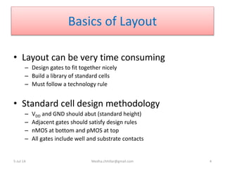
  • 4. Basics of Layout • Layout can be very time consuming – Design gates to fit together nicely – Build a library of standard cells – Must follow a technology rule • Standard cell design methodology – VDD and GND should abut (standard height) – Adjacent gates should satisfy design rules – nMOS at bottom and pMOS at top – All gates include well and substrate contacts 5-Jul-14 [email protected] 4
  • 5. What Are Layout Extractors?? • Once the layout is made, there always is parasitic capacitances and resistances associated with the design. • This is because of the compact layouts to make the chips smaller. More you make compact layout more will it introduce these parasitic components. • These interferes in the functioning and performance of the circuit in terms of timing, speed and power consumption. 5-Jul-14 [email protected] 5
  • 6. Contd… • Examine the inter-relationship of mask layers to infer the existence of transistors and other components • Related to Design Rule Checkers – Design-rule Verification • Some form of layout extraction is usually done to create data for back annotation 5-Jul-14 [email protected] 6
  • 7. Tools used for Extraction • FastCap, FastHenry • Star-RCXT • QRC • Calibre xACT3D etc… 5-Jul-14 [email protected] 7
  • 8. Steps to Extract a Layout • Create Layout Cellview • Design Rule Checking • Layout Parameter Extraction • Layout vs. Schematic Comparison 5-Jul-14 Courtesy:http://www.egr.msu.edu/classes/ece410/mason/files/TutorialB.pdf 8
  • 9. Step1: Create Layout Cellview From the schematic, we can draw the layout cellview From the Library Manager window, Select File => New => Cellview (Virtuoso is the main layout editor of Cadence design tools) 5-Jul-14 [email protected] 9
  • 10. Step2:Design Rule Checking • After you have finished your layout, an automatic program will check each and every polygon in your design against these design rules and report violations. This process is called Design Rule Checking (DRC) and MUST be done for every layout to ensure it will function properly when fabricated. • After the DRC is complete, the bottom line in the CIW(Command Interpreter Window) will show “# Total errors found” • The DRC will be successful when you see the results saying “0 Total errors found” 5-Jul-14 [email protected] 10
  • 11. Step3: Layout Parameter Extraction • mask layout contains only physical data • Extraction process identifies the devices from the layout and generates a SPICE-like netlist and other files necessary to complete the design process • In the Virtuoso Layout Editing window select Verify => Extract 5-Jul-14 [email protected] 11
  • 13. Conclusion 5-Jul-14 [email protected] 13 Data Preparation Draw Schematic (Virtuoso) Logic Simulation (Verilog-XL) Pre-layout Simulation (Spectre) Layout (Virtuoso) Design Rule Check (Calibre) Layout Versus Schematic Check (Calibre) Extraction (Calibre) Post layout simulation (HSPICE)

Editor's Notes

  • #7: Back Annotation: Once a layout has been constructed and there is isomorphism between schematic n/w and layout n/w, one can correlate extracted capacitances from the layout with the schematic and perform simulation or timing analysis to verify performance. This is done by moving the capacitance that appears on a layout node to the corresponding schematic node while accounting for existing capacitance on the schematic node. For instance, the schematic may already have source-drain and gate load due to gates connected to the node and only routing capacitance is required to be added. This operation is called “Back-Annotation”.