Chapter 8 Embedded Hardware Design and Development (third portion)
Download as PPTX, PDF4 likes3,987 views

This document contains lecture slides for a chapter on embedded hardware design and development from a textbook on embedded systems. It covers topics like analog and digital electronic components, integrated circuit design, electronic design automation tools, and using the Eagle EDA tool for schematic design and PCB layout. The learning objectives are to learn about embedded hardware elements and design principles, refresh knowledge on basic analog and digital components, and learn about integrated circuit design and EDA tools.


![Mandalay Technological University
Department of Computer Engineering and Information Technology
Lecture Slides for Textbook Introduction to Embedded Systems, Moe Moe Myint, 2017-2018
Combinational vs Sequential Logic Circuits
Combinational Logic Circuits Sequential Logic Circuits
Output is a function of the present inputs (Time
Independent Logic).
Output is a function of clock, present inputs and the
previous states of the system.
Do not have the ability to store data (state). Have memory to store the present states that is sent
as control input (enable) for the next operation.
It does not require any feedback. It simply outputs
the input according to the logic designed.
It involves feedback from output to input that is
stored in the memory for the next operation.
Used mainly for Arithmetic and Boolean operations. Used for storing data (and hence used in RAM).
Logic gates are the elementary building blocks. Flip flops (binary storage device) are the elementary
building unit.
Independent of clock and hence does not require
triggering to operate.
Clocked (Triggered for operation with electronic
pulses).
Example: Adder [1+0=1; Dependency only on
present inputs i.e., 1 and 0].
Example: Counter [Previous O/P+1=Current O/P;
Dependency on present input as well as previous
state].](https://image.slidesharecdn.com/chapter8thirdportion-student-180710032812/85/Chapter-8-Embedded-Hardware-Design-and-Development-third-portion-21-320.jpg)


Chapter 8 Embedded Hardware Design and Development (third portion)
- 1. Introduction to EMBEDDED SYSTEM (2nd Edition) SHIBU K V Dr Moe Moe Myint Department of Computer Engineering & Information Technology Mandalay Technological University www.slideshare.net/MoeMoeMyint [email protected] drmoemoemyint.blogspot.com IT-52061 Chapter 8 Embedded Hardware Design and Development
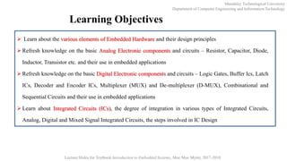
- 2. Learning Objectives Learn about the various elements of Embedded Hardware and their design principles Refresh knowledge on the basic Analog Electronic components and circuits – Resistor, Capacitor, Diode, Inductor, Transistor etc. and their use in embedded applications Refresh knowledge on the basic Digital Electronic components and circuits – Logic Gates, Buffer Ics, Latch ICs, Decoder and Encoder ICs, Multiplexer (MUX) and De-multiplexer (D-MUX), Combinational and Sequential Circuits and their use in embedded applications Learn about Integrated Circuits (ICs), the degree of integration in various types of Integrated Circuits, Analog, Digital and Mixed Signal Integrated Circuits, the steps involved in IC Design Mandalay Technological University Department of Computer Engineering and Information Technology Lecture Slides for Textbook Introduction to Embedded Systems, Moe Moe Myint, 2017-2018
- 3. Outlines Analog Electronic Components 229 (Roll no.1) Digital Electronic Components 230 (Roll no. 2,3,4,5,6,7,8,9,10,11) VLSI and Integrated Circuit Design 243 (Roll no. 12, 13,14) Electronic Design Automation (EDA) Tools 248 How to use the Eagle EDA Tool? 249 Schematic Design using Eagle Capture CIS 249 The PCB Layout Design 267 Printed Circuit Board (PCB) Fabrication 288 Mandalay Technological University Department of Computer Engineering and Information Technology Lecture Slides for Textbook Introduction to Embedded Systems, Moe Moe Myint, 2017-2018 3 Finished
- 4. Mandalay Technological University Department of Computer Engineering and Information Technology Lecture Slides for Textbook Introduction to Embedded Systems, Moe Moe Myint, 2017-2018 LogicGateSimulation
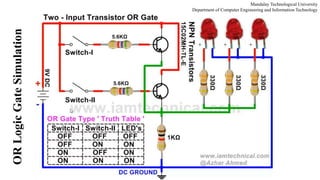
- 5. Mandalay Technological University Department of Computer Engineering and Information Technology Lecture Slides for Textbook Introduction to Embedded Systems, Moe Moe Myint, 2017-2018 ORLogicGateSimulation
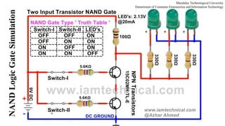
- 6. Mandalay Technological University Department of Computer Engineering and Information Technology Lecture Slides for Textbook Introduction to Embedded Systems, Moe Moe Myint, 2017-2018 NANDLogicGateSimulation
- 7. Mandalay Technological University Department of Computer Engineering and Information Technology Lecture Slides for Textbook Introduction to Embedded Systems, Moe Moe Myint, 2017-2018 NORLogicGateSimulation
- 8. Mandalay Technological University Department of Computer Engineering and Information Technology Lecture Slides for Textbook Introduction to Embedded Systems, Moe Moe Myint, 2017-2018 NOTLogicGateSimulation
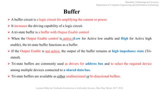
- 9. Mandalay Technological University Department of Computer Engineering and Information Technology Lecture Slides for Textbook Introduction to Embedded Systems, Moe Moe Myint, 2017-2018 Buffer A buffer circuit is a logic circuit for amplifying the current or power. It increases the driving capability of a logic circuit. A tri-state buffer is a buffer with Output Enable control. When the Output Enable control is active (Low for Active low enable and High for Active high enable), the tri-state buffer functions as a buffer. If the Output Enable is not active, the output of the buffer remains at high impedance state (Tri- stated). Tri-state buffers are commonly used as drivers for address bus and to select the required device among multiple devices connected to a shared data bus. Tri-state buffers are available as either unidirectional or bi-directional buffers.
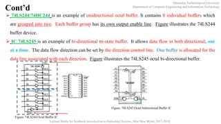
- 10. Mandalay Technological University Department of Computer Engineering and Information Technology Lecture Slides for Textbook Introduction to Embedded Systems, Moe Moe Myint, 2017-2018 Cont’d 74LS244/74HC244 is an example of unidirectional octal buffer. It contains 8 individual buffers which are grouped into two. Each buffer group has its own output enable line. Figure illustrates the 74LS244 buffer device. IC 74LS245 is an example of bi-directional tri-state buffer. It allows data flow in both directional, one at a time. The data flow direction can be set by the direction control line. One buffer is allocated for the data line associated with each direction. Figure illustrates the 74LS245 octal bi-directional buffer. Figure. 74LS244 Octal Buffer IC Figure. 74LS245 Octal bidirectional Buffer IC
- 11. Mandalay Technological University Department of Computer Engineering and Information Technology Lecture Slides for Textbook Introduction to Embedded Systems, Moe Moe Myint, 2017-2018 Decoder A decoder is a logic circuit which generates all the possible combinations of the input signals. Decoders are named with their input line numbers and the possible combinations of the input as output. Examples are 2 to 4 decoder, 3 to 8 decoder and 4 to 16 decoder. The 3 to 8 decoder contains 3 input signal lines and it is possible to have 8 different configurations with the 3 lines (000 to 111 in the input line corresponds to 0 to 7 in the output line). Depending on the input signal, the corresponding output line is asserted. For example, for the input state 001, the output line 2 is asserted. Decoders are mainly used for address decoding and chip select signal generation in electronic circuits and are available as integrated circuits. 74LS138/74AHC138 is an example for 3 to 8 decoder IC. Figure illustrates the 74AHC138 decoder and the function table for it.
- 12. Mandalay Technological University Department of Computer Engineering and Information Technology Lecture Slides for Textbook Introduction to Embedded Systems, Moe Moe Myint, 2017-2018 Cont’d The decoder output is enabled only when the ‘Output Enable’ signal lines E1, E2 and E3 are at logic levels 0, 0 and 1 respectively. If the output-enable signals are not at the required logic state, all the output lines are forced to the inactive (High) state. The output line corresponding to the input state is asserted ‘Low’ when the ‘Output Enable’ signal lines are at the required logic state (Here E1=E2=0 and E3=1). The output line can be directly connected to the chip select pin of a device, if the chip select logic of the device is active low.
- 13. Mandalay Technological University Department of Computer Engineering and Information Technology Lecture Slides for Textbook Introduction to Embedded Systems, Moe Moe Myint, 2017-2018 Cont’d Inputs Output Enable Select E1 E2 E3 A2 A1 A0 O0 O1 O2 O3 O4 O5 O6 O7 0 0 1 0 0 0 0 1 1 1 1 1 1 1 0 0 1 0 0 1 1 0 1 1 1 1 1 1 0 0 1 0 1 0 1 1 0 1 1 1 1 1 0 0 1 0 1 1 1 1 1 0 1 1 1 1 0 0 1 1 0 0 1 1 1 1 0 1 1 1 0 0 1 1 0 1 1 1 1 1 1 0 1 1 0 0 1 1 1 0 1 1 1 1 1 1 0 1 0 0 1 1 1 1 1 1 1 1 1 1 1 0
- 14. Mandalay Technological University Department of Computer Engineering and Information Technology Lecture Slides for Textbook Introduction to Embedded Systems, Moe Moe Myint, 2017-2018 Encoder An encoder performs the reverse operation of decoder. The encoder encodes the corresponding input state to a particular output format. The binary encoder encodes the input to the corresponding binary format. Encoders are named with their input line numbers and the encoder output format. Examples are 4 to 2 encoder, 8 to 3 encoder and 16 to 4 encoder. The 8 to 3 encoder contains 8 input signal lines and it is possible to generate a 3 bit binary output corresponding to the input (e.g. inputs 0 to 7 are encoded to binary 111 to 000 in the output lines). The corresponding output line is asserted in accordance with the input signals. For example, if the input line 1 is asserted, the output lines A0, A1 and A2 are asserted as 0, 1 and 1 respectively. Encoders are mainly used for address decoding and chip select signal generating in electronic circuits and are available as integrated circuits. 74F148/74LS148 is an example of 8 to 3 encoder IC. Figure illustrates the 74F148/74LS148 encoder and the function table for it.
- 15. Mandalay Technological University Department of Computer Engineering and Information Technology Lecture Slides for Textbook Introduction to Embedded Systems, Moe Moe Myint, 2017-2018 Cont’d Input Select Output 7 6 5 4 3 2 1 0 E1 GS E0 A2 A1 A0 1 1 1 1 1 1 1 0 0 0 1 1 1 1 1 1 1 1 1 1 0 1 0 0 1 1 1 0 1 1 1 1 1 0 1 1 0 0 1 1 0 1 1 1 1 1 0 1 1 1 0 0 1 1 0 0 1 1 1 0 1 1 1 1 0 0 1 0 1 1 1 1 0 1 1 1 1 1 0 0 1 0 1 0 1 0 1 1 1 1 1 1 0 0 1 0 0 1 0 1 1 1 1 1 1 1 0 0 1 0 0 0
- 16. Mandalay Technological University Department of Computer Engineering and Information Technology Multiplexer (MUX) A multiplexer (MUX) can be considered as a digital switch which contains multiple input lines and a single output line. The inputs of a MUX are said to be multiplexed. It is a digital circuit which selects one of the n data inputs and routes it to the output. 74S151 is an example for 8 to 1 multiplexer IC. Figure illustrates the 74S151 multiplexer and the function table for it. Lecture Slides for Textbook Introduction to Embedded Systems, Moe Moe Myint, 2017-2018 Figure. 8 to 1 multiplexer IC and I/O signal states
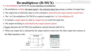
- 17. Mandalay Technological University Department of Computer Engineering and Information Technology Lecture Slides for Textbook Introduction to Embedded Systems, Moe Moe Myint, 2017-2018 De-multiplexer (D-MUX) A de-multiplexer performs the reverse operation of multiplexer. De-multiplexer switches the input signal to the selected output line among a number of output lines. The output line to which the input is to be switched is selected by the output selector control lines. The 1 to 2 de-multiplexer, NL7SZ18 is a typical example for 1 to 2 de-multiplexer IC. It contains a single input line and two output lines to switch the input line. The output switching is controlled by the output selector control. Figure illustrates the NL7SZ18 de-multiplexer and the function table for it. When one output line is selected by the output selector control (S), the other output line remains in the High impedance state.
- 18. Mandalay Technological University Department of Computer Engineering and Information Technology Lecture Slides for Textbook Introduction to Embedded Systems, Moe Moe Myint, 2017-2018 Combinational Circuits In digital system design, a combinational circuit is a combination of the different logic gates. The output of the combinational circuit is dependent only on the present state of the inputs at the given point of time. The combinational circuit do not use any memory. Encoders, decoders, multiplexers, de-multiplexers, adder circuits, comparators, multiple input gates, etc. are examples of digital combinational circuits. A combinational circuit can have an n number of inputs and m number of outputs
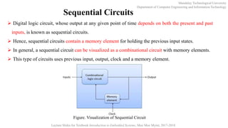
- 19. Mandalay Technological University Department of Computer Engineering and Information Technology Lecture Slides for Textbook Introduction to Embedded Systems, Moe Moe Myint, 2017-2018 Sequential Circuits Digital logic circuit, whose output at any given point of time depends on both the present and past inputs, is known as sequential circuits. Hence, sequential circuits contain a memory element for holding the previous input states. In general, a sequential circuit can be visualized as a combinational circuit with memory elements. This type of circuits uses previous input, output, clock and a memory element. Figure. Visualization of Sequential Circuit
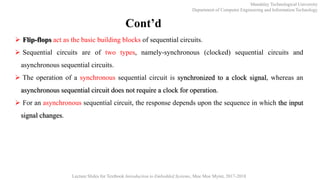
- 20. Mandalay Technological University Department of Computer Engineering and Information Technology Lecture Slides for Textbook Introduction to Embedded Systems, Moe Moe Myint, 2017-2018 Cont’d Flip-flops act as the basic building blocks of sequential circuits. Sequential circuits are of two types, namely-synchronous (clocked) sequential circuits and asynchronous sequential circuits. The operation of a synchronous sequential circuit is synchronized to a clock signal, whereas an asynchronous sequential circuit does not require a clock for operation. For an asynchronous sequential circuit, the response depends upon the sequence in which the input signal changes.
- 21. Mandalay Technological University Department of Computer Engineering and Information Technology Lecture Slides for Textbook Introduction to Embedded Systems, Moe Moe Myint, 2017-2018 Combinational vs Sequential Logic Circuits Combinational Logic Circuits Sequential Logic Circuits Output is a function of the present inputs (Time Independent Logic). Output is a function of clock, present inputs and the previous states of the system. Do not have the ability to store data (state). Have memory to store the present states that is sent as control input (enable) for the next operation. It does not require any feedback. It simply outputs the input according to the logic designed. It involves feedback from output to input that is stored in the memory for the next operation. Used mainly for Arithmetic and Boolean operations. Used for storing data (and hence used in RAM). Logic gates are the elementary building blocks. Flip flops (binary storage device) are the elementary building unit. Independent of clock and hence does not require triggering to operate. Clocked (Triggered for operation with electronic pulses). Example: Adder [1+0=1; Dependency only on present inputs i.e., 1 and 0]. Example: Counter [Previous O/P+1=Current O/P; Dependency on present input as well as previous state].
- 22. Mandalay Technological University Department of Computer Engineering and Information Technology Lecture Slides for Textbook Introduction to Embedded Systems, Moe Moe Myint, 2017-2018 Difference between Synchronous and Asynchronous Sequential Circuits Synchronous Sequential Circuit Asynchronous Sequential Circuit Clocked flip-flops act as the memory element in the circuit. All flip-flops are clocked to the same clock signal. Un-clocked flip-flops or logic gate circuits with feedback loops act as the memory element in the circuit. The output state of the circuit changes only with clock trigger. The output state change happens instantaneously with changes in input state. The speed of operation depends on the maximum supported clock frequency. Faster than synchronous sequential circuits.
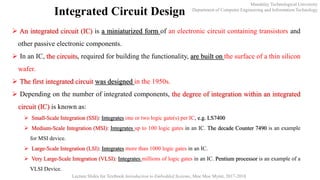
- 23. Mandalay Technological University Department of Computer Engineering and Information Technology Lecture Slides for Textbook Introduction to Embedded Systems, Moe Moe Myint, 2017-2018 Integrated Circuit Design An integrated circuit (IC) is a miniaturized form of an electronic circuit containing transistors and other passive electronic components. In an IC, the circuits, required for building the functionality, are built on the surface of a thin silicon wafer. The first integrated circuit was designed in the 1950s. Depending on the number of integrated components, the degree of integration within an integrated circuit (IC) is known as: Small-Scale Integration (SSI): Integrates one or two logic gate(s) per IC, e.g. LS7400 Medium-Scale Integration (MSI): Integrates up to 100 logic gates in an IC. The decade Counter 7490 is an example for MSI device. Large-Scale Integration (LSI): Integrates more than 1000 logic gates in an IC. Very Large-Scale Integration (VLSI): Integrates millions of logic gates in an IC. Pentium processor is an example of a VLSI Device.
- 24. Mandalay Technological University Department of Computer Engineering and Information Technology Lecture Slides for Textbook Introduction to Embedded Systems, Moe Moe Myint, 2017-2018 Different Types of IC Design Depending on the type of circuits integrated in the IC, the IC design is categorized as: Digital Design: Deals with the design of integrated circuits handling digital signals and data. The I/O requirement for such an IC is always digital. Microprocessor/microcontroller, memory, etc. are examples of digital data. Analog Design: Deals with the design of integrated circuits handling analog signals and data. Analog design gives more emphasis to the physics aspects of semiconductor devices such as gain, power dissipation, resistance, etc. RF IC design, Op-Amp design, voltage regulator IC design, etc. are examples for Analog IC Design. Mixed Signal Design: In today’s world, most of the applications require the co-existence of digital signals and analog signals for functioning. Mixed signal design involves design of ICs, which handle both digital and analog signals as well as data. Design of an analog-to-digital converter is an example for mixed signal IC design.
- 25. Mandalay Technological University Department of Computer Engineering and Information Technology Lecture Slides for Textbook Introduction to Embedded Systems, Moe Moe Myint, 2017-2018 Various Steps Involved in a HDL Based Design Figure. The HDL based VLSI Design Process VHDL or Verilog Description Functional Simulation Synthesis Placement and Routing Timing Simulation Area and Timing Constraints Technology Library 1234
- 26. Mandalay Technological University Department of Computer Engineering and Information Technology Lecture Slides for Textbook Introduction to Embedded Systems, Moe Moe Myint, 2017-2018 Objective Questions 1. The logic expression 𝑌 = 𝐴B + A 𝐵 represents the logic gate (a) AND (b) NAND (c) OR (d) XOR (e) NOR 2. Which of the following is an example for Buffer IC? (a) 74LS00 (b) 74LS244 (c) 74LS08 (d) 74LS373 (e) None of these 3. Which of the following digital circuits is used for selecting one input from a set of inputs and connecting it to an output line (a) Buffer (b) Latch (d) Multiplexer (e) De-Multiplexer (f) None of these 4. Combinational circuits contain a memory element. State True or False. (a) True (b) False 5. Half Adder is an example of Sequential circuit. State True or False. (a) True (b) False
- 27. Mandalay Technological University Department of Computer Engineering and Information Technology Lecture Slides for Textbook Introduction to Embedded Systems, Moe Moe Myint, 2017-2018 Review Questions 1. Explain the role of de-coders in embedded hardware development. Explain the functioning of the circuit. 2. What is a combinational circuit? Draw a combinational circuit for embedded application development. 3. What is sequential circuit? Draw a sequential circuit and explain its functioning. 4. Explain the difference between digital combinational and sequential circuits. 5. Explain the difference between synchronous and asynchronous sequential circuits. 6. What is an Integrated Circuit (IC)? Explain the different types of integrations for ICs. Give an example for each. 7. Explain the different types of IC design. Give an example for each. 8. Explain the different steps involved in VHDL based IC design.
- 28. Only Original Owner has full rights reserved for copied images. This PPT is only for fair academic use. 28 Mandalay Technological University Department of Computer Engineering and Information Technology Lecture Slides for Textbook Introduction to Embedded Systems, Moe Moe Myint, 2017-2018
- 29. 29
Editor's Notes
- #5: A buffer amplifier (sometimes simply called a buffer) is one that provides electrical impedance transformation from one circuit to another, with the aim of preventing the signal source from being affected by whatever currents (or voltages, for a current buffer) that the load may produce. The signal is 'buffered from' load currents. Two main types of buffer exist: the voltage buffer and the current buffer
- #6: A buffer amplifier (sometimes simply called a buffer) is one that provides electrical impedance transformation from one circuit to another, with the aim of preventing the signal source from being affected by whatever currents (or voltages, for a current buffer) that the load may produce. The signal is 'buffered from' load currents. Two main types of buffer exist: the voltage buffer and the current buffer
- #7: A buffer amplifier (sometimes simply called a buffer) is one that provides electrical impedance transformation from one circuit to another, with the aim of preventing the signal source from being affected by whatever currents (or voltages, for a current buffer) that the load may produce. The signal is 'buffered from' load currents. Two main types of buffer exist: the voltage buffer and the current buffer
- #8: A buffer amplifier (sometimes simply called a buffer) is one that provides electrical impedance transformation from one circuit to another, with the aim of preventing the signal source from being affected by whatever currents (or voltages, for a current buffer) that the load may produce. The signal is 'buffered from' load currents. Two main types of buffer exist: the voltage buffer and the current buffer
- #9: A buffer amplifier (sometimes simply called a buffer) is one that provides electrical impedance transformation from one circuit to another, with the aim of preventing the signal source from being affected by whatever currents (or voltages, for a current buffer) that the load may produce. The signal is 'buffered from' load currents. Two main types of buffer exist: the voltage buffer and the current buffer
- #10: - amplify the voltage / current of production of the logic circuit A buffer amplifier (sometimes simply called a buffer) is one that provides electrical impedance transformation from one circuit to another, with the aim of preventing the signal source from being affected by whatever currents (or voltages, for a current buffer) that the load may produce. The signal is 'buffered from' load currents. Two main types of buffer exist: the voltage buffer and the current buffer
- #12: 4 to 16 line decoder activates one of 16 outputs for each 4 bit input in the integer range [0,15]. A decoder is a combinational logic circuit which is used to change the code into a set of signals. It is the reverse process of an encoder. A decoder circuit takes multiple inputs and gives multiple outputs. A decoder circuit takes binary data of ‘n’ inputs ito ‘2^n’ unique output. In addition to input pins, the decoder has a enable pin.. It has n input and to a maximum m = 2n outputs. Decoder is identical to a demultiplexer without any data input. It performs operations which are exactly opposite to those of an encoder. Examples of Decoders are following. Code converters BCD to seven segment decoders Nixie tube decoders Relay actuator Example of an embedded system The digital audio/video decoding system, called the A/V decoder, which is an integral part of the DST, is an embedded system. The A/V decoder accepts a single multimedia stream and produces sound and video frames as output. The signals received from the satellite by the DST contain multiple streams or channels. Therefore, the A/V decoder works in conjunction with the transport stream decoder, which is yet another embedded system. The transport stream decoder de-multiplexes the incoming multimedia streams into separate channels and feeds only the selected channel to the A/V decoder.
- #13: 74AHC138 is a 3 to 8 line decoder/demultiplexer. It accepts three binary weighted address inputs (A0, A1 and A2). When enabled, it provides eight mutually exclusive outputs (Y\0 to Y\7) that are LOW when selected. There are three enable inputs: two active LOW(E\1 and E\2) and one active HIGH (E3). Every output is HIGH usless E\1 and E\2 are LOW and E3 is HIGH. 3 to 8 decoder 3 line to 8 line decoder : this decoder circuit gives 8 logic outputs for 3 inputs and has a enable pin. 2 to 4 Line Decoder The block diagram of 2 to 4 line decoder is shown in the fig. A and B are the two inputs where D through D are the four outputs. Truth table explains the operations of a decoder. It shows that each output is 1 for only a specific combination of inputs.
- #14: Note that all three enables (E1, E2 and E3) must be active, e.g. low, low and high, respectively… Each output of the decoder can be attached to an 2764 EPROM (8K X 8)
- #15: Encoder is a combinational circuit which is designed to perform the inverse operation of the decoder. An encoder has n number of input lines and m number of output lines. An encoder produces an m bit binary code corresponding to the digital input number. The encoder accepts an n input digital word and converts it into an m bit another digital word. Examples of Encoders are following. Priority encoders Decimal to BCD encoder Octal to binary encoder Hexadecimal to binary encoder
- #16: Note that all three enables (E1, E2 and E3) must be active, e.g. low, low and high, respectively… Each output of the decoder can be attached to an 2764 EPROM (8K X 8)
- #17: Multiplexer is a special type of combinational circuit. There are n-data inputs, one output and m select inputs with 2m = n. It is a digital circuit which selects one of the n data inputs and routes it to the output. The selection of one of the n inputs is done by the selected inputs. Depending on the digital code applied at the selected inputs, one out of n data sources is selected and transmitted to the single output Y. E is called the strobe or enable input which is useful for the cascading. It is generally an active low terminal that means it will perform the required operation when it is low. Multiplexers come in multiple variations 2 : 1 multiplexer 4 : 1 multiplexer 16 : 1 multiplexer 32 : 1 multiplexer
- #18: A demultiplexer performs the reverse operation of a multiplexer i.e. it receives one input and distributes it over several outputs. It has only one input, n outputs, m select input. At a time only one output line is selected by the select lines and the input is transmitted to the selected output line. A de-multiplexer is equivalent to a single pole multiple way switch as shown in fig. Demultiplexers comes in multiple variations. 1 : 2 demultiplexer 1 : 4 demultiplexer 1 : 16 demultiplexer 1 : 32 demultiplexer
- #19: Combinational Logic Circuits are made up from basic logic NAND, NOR or NOT gates that are ‘combined’ or connected together to produce more complicated switching circuits.
- #20: What is a combinational circuit? Draw a combinational circuit for embedded application development. This type of circuits uses previous input, output, clock and a memory element.
- #21: Flip flop is a sequential circuit which generally samples its inputs and changes its outputs only at particular instants of time and not continuously. Flip flop is said to be edge sensitive or edge triggered rather than being level triggered like latches. S-R Flip Flop It is basically S-R latch using NAND gates with an additional enable input. It is also called as level triggered SR-FF. For this, circuit in output will take place if and only if the enable input (E) is made active. In short this circuit will operate as an S-R latch if E = 1 but there is no change in the output if E = 0.
- #22: Combinational and sequential circuits are the most essential concepts to be understood in digital electronics. Combinational logic (sometimes also referred to as time-independent logic) is a type of digital logic which is implemented by Boolean circuits, where the output is a pure function of the present input only. Sequential logic is a type of logic circuit whose output depends not only on the present value of its input signals but on the sequence of past inputs. To design sequential circuit also we use gates. But in case of sequential circuit we use feedback gates (memory elements) alogn with combinational logic. SO that it can work like a latch or flip-flop.
- #23: 8. Explain the difference between synchronous and asynchronous sequential circuits. Give an example for both. Synchronous Sequential Circuit Asynchronous Sequential Circuit It is easy to design. It is difficult to design. A clocked flip flop acts as memory element. An unclocked flip flop or time delay is used as memory element. They are slower as clock is involved. They are comparatively faster as no clock is used here. The states of memory element is affected only at active edge of clock, if input is changed. The states of memory element will change any time as soon as input is changed.
- #24: Miniaturized producing small form
- #25: Miniaturized producing small form
- #26: Miniaturized producing small form