SlideShare a Scribd company logo
1
Presented by
Mrs. Bandana Mallick
UNIT-III
Combinational MOS Logic
Circuits
2
• Introduction
• MOS logic circuits with depletion nMos loads
 2-input NOR gate
2-input NAND gate
• CMOS logic circuits
Outline
3
• A combinational circuit consists of input variables, logic gates, and output
variables. In this type of logic circuits outputs depend only on the current
inputs.
• Each output function expressed in terms of the (n) input variables.
4
5
MOS logic circuits with depletion nMos loads
6
When VA=VB=high then transistor turns on & provides a conducting
path between output node & ground. Hence
Vout= low.
When both input voltages VA and VB are lower than the
corresponding driver threshold voltage, the driver transistor are
turned off and conduct no drain current.
Consequently, the load device, which operates in the linear region,
also has zero drain current. In particular, its linear region current
equation becomes
VDD- VOH = 0
VOH= VDD
7
8
9
10
CMOS logic gate concept:
11
12
13
For PMOS,
MpA:Linear,
MpB: saturation
14
LAYOUT
DIAGRAM
15
16
17
18
Complex logic circuits
19
20
21
22
23
Optimized stick diagram layout of complex cmos logic gate
24
25
26
27
28
29
30
31
32
33
34
35
Unit 3
Chapter-2
36
Sequential logic circuit is a logic circuit in which the output is
determined by the current inputs as well as the previously applied
input variables.
A sequential circuit consisting of a combinational circuit and a
memory block in the feedback loop .
37
The critical components of sequential systems are the basic regenerative
circuits, which can be classified into three main groups:
Bistable circuits,
Monostable circuits,
and Astable circuits.
The general classification of non-regenerative and regenerative logic circuits is
shown in Fig.
38
The basic bistable element consists of two identical cross-coupled inverter
circuits as shown in figure:
39
Figure shows the circuit diagram of a CMOS two-inverter bistable element.
At the unstable operating point of this
circuit, all four transistors are in
saturation, resulting in maximum loop
gain for the circuit. If the initial operating
condition is set at this point, any small
voltage perturbation will cause
significant changes in the operating
modes of the transistors. Thus, we
expect the output voltages of the two
inverters to diverge and eventually settle
at VOH and VOL, respectively.
40
If the set input (S) is equal to logic "1" and the reset input is equal to
logic "0," then the output node Q will be forced to logic " 1 " while the
output node Q is forced to logic "0." This means that the SR latch will
be set, regardless of its previous state.
Similarly, if S is equal to "0" and R is equal to " 1," then the output
node Q will be forced to "0" while Q’ is forced to "1." Thus, with this
input combination, the latch is reset, regardless of its previously held
state. Finally, consider the case in which both of the inputs S and R are
equal to logic “1 ." In this case, both output nodes will be forced to
logic "0," which conflicts with the complementarily of Q and Q’.
Therefore, this input combination is not permitted during normal
operation and is considered to be a not allowed condition.
41
42
43
The operation of the CMOS SR latch circuit can be examined in more
detail by considering the operating modes of the four nMOS
transistors, MI, M2,M3, and M4. If the set input (S) is equal to VOH
and the reset input (R) is equal to VOL,both of the parallel-connected
transistors Ml and M2 will be on.
Depletion-load nMOS SR latch circuit
based on NOR2 gates.
44
SR Latch based on NAND Gate
The small circles at the S and R input
terminals represents that the circuit
responds to active low input signals.
45
Truth table of CMOS SR latch
using NAND gate
if S is equal to "0”and R is equal to " 1," the output Q attains a logic " 1 "
value and the complementary output Q becomes logic "0." Thus, in order
to set the NAND SR latch, a logic "0" must be applied to the set (S) input.
Similarly, in order to reset the latch, a logic "0" must be applied to the
reset (R) input. The conclusion is that the NAND-based SR latch responds
to active low input signals, as opposed to the NOR-based SR latch, which
responds to active high inputs.
46
47
Depletion-load nMOS NAND-based SR
latch circuit.
48
Clocked SR Latch
The clock pulse will be assumed to be a periodic square waveform, which is
applied simultaneously to all clocked logic gates in the system.
Gate-level schematic of the clocked NOR-
based SR latch.
49
Thank
You

More Related Content

Similar to Combinational Circuit_vlsi desgin_timing analysis (20)

PPT
Hardware combinational
Defri Tan
 
DOC
Double tail comparator
MdLogic Mdls
 
PDF
Lect2 up140 (100325)
aicdesign
 
PDF
Data converter modelingの参考資料2
Tsuyoshi Horigome
 
PDF
STUCK-OPEN FAULT ANALYSIS IN CMOS TRANSISTOR BASED COMBINATIONAL CIRCUITS
Minh Anh Nguyen
 
PDF
STUCK-OPEN FAULT ANALYSIS IN CMOS TRANSISTOR BASED COMBINATIONAL CIRCUITS
Minh Anh Nguyen
 
PPT
Combinational Logic
Sirat Mahmood
 
PPTX
CMOS Logic
Sudhanshu Janwadkar
 
PDF
cmoslogic_data7.pdf
kalivaraprasad2
 
DOCX
Logic design alexander1 christopher
world_chris
 
PDF
Cmos logic
Revathi Subramaniam
 
PPTX
ELN Presentation Add more information to your upload.pptx
MohammedAdnankhan4
 
PDF
Chapter 1: Circuit Characterization Of CMOS Circuits.pdf
j2yshjzzsx
 
PDF
CMOS Topic 5 -_cmos_inverter
Ikhwan_Fakrudin
 
PPT
Logic Gate
Công Mai Văn
 
PPTX
Elecrical Propertiesddfafafafafafafav.pptx
rajukolluri
 
PPTX
cmos vlsi design for b.tech 4th year students
KUNTALADAS5
 
PDF
Chap16-1-NMOS-Inverter.pdf
ahmedsalim244821
 
PPTX
Logic families ppt eceb srp
Saikat Dutt
 
PDF
vlsi 2 unit.pdfvlsi unit 2 important notes for ece department
nitcse
 
Hardware combinational
Defri Tan
 
Double tail comparator
MdLogic Mdls
 
Lect2 up140 (100325)
aicdesign
 
Data converter modelingの参考資料2
Tsuyoshi Horigome
 
STUCK-OPEN FAULT ANALYSIS IN CMOS TRANSISTOR BASED COMBINATIONAL CIRCUITS
Minh Anh Nguyen
 
STUCK-OPEN FAULT ANALYSIS IN CMOS TRANSISTOR BASED COMBINATIONAL CIRCUITS
Minh Anh Nguyen
 
Combinational Logic
Sirat Mahmood
 
cmoslogic_data7.pdf
kalivaraprasad2
 
Logic design alexander1 christopher
world_chris
 
ELN Presentation Add more information to your upload.pptx
MohammedAdnankhan4
 
Chapter 1: Circuit Characterization Of CMOS Circuits.pdf
j2yshjzzsx
 
CMOS Topic 5 -_cmos_inverter
Ikhwan_Fakrudin
 
Logic Gate
Công Mai Văn
 
Elecrical Propertiesddfafafafafafafav.pptx
rajukolluri
 
cmos vlsi design for b.tech 4th year students
KUNTALADAS5
 
Chap16-1-NMOS-Inverter.pdf
ahmedsalim244821
 
Logic families ppt eceb srp
Saikat Dutt
 
vlsi 2 unit.pdfvlsi unit 2 important notes for ece department
nitcse
 

Recently uploaded (20)

PDF
Design Thinking basics for Engineers.pdf
CMR University
 
PDF
Pressure Measurement training for engineers and Technicians
AIESOLUTIONS
 
PDF
Viol_Alessandro_Presentazione_prelaurea.pdf
dsecqyvhbowrzxshhf
 
PDF
AI TECHNIQUES FOR IDENTIFYING ALTERATIONS IN THE HUMAN GUT MICROBIOME IN MULT...
vidyalalltv1
 
PDF
Basic_Concepts_in_Clinical_Biochemistry_2018كيمياء_عملي.pdf
AdelLoin
 
PPTX
MATLAB : Introduction , Features , Display Windows, Syntax, Operators, Graph...
Amity University, Patna
 
PPTX
Damage of stability of a ship and how its change .pptx
ehamadulhaque
 
PDF
Halide Perovskites’ Multifunctional Properties: Coordination Engineering, Coo...
TaameBerhe2
 
DOCX
8th International Conference on Electrical Engineering (ELEN 2025)
elelijjournal653
 
PDF
Biomechanics of Gait: Engineering Solutions for Rehabilitation (www.kiu.ac.ug)
publication11
 
PDF
MAD Unit - 1 Introduction of Android IT Department
JappanMavani
 
DOC
MRRS Strength and Durability of Concrete
CivilMythili
 
PDF
MAD Unit - 2 Activity and Fragment Management in Android (Diploma IT)
JappanMavani
 
PPTX
Presentation 2.pptx AI-powered home security systems Secure-by-design IoT fr...
SoundaryaBC2
 
PPTX
Introduction to Design of Machine Elements
PradeepKumarS27
 
PPTX
Lecture 1 Shell and Tube Heat exchanger-1.pptx
mailforillegalwork
 
PPTX
Shinkawa Proposal to meet Vibration API670.pptx
AchmadBashori2
 
PPTX
Heart Bleed Bug - A case study (Course: Cryptography and Network Security)
Adri Jovin
 
PPTX
Element 11. ELECTRICITY safety and hazards
merrandomohandas
 
PPTX
Big Data and Data Science hype .pptx
SUNEEL37
 
Design Thinking basics for Engineers.pdf
CMR University
 
Pressure Measurement training for engineers and Technicians
AIESOLUTIONS
 
Viol_Alessandro_Presentazione_prelaurea.pdf
dsecqyvhbowrzxshhf
 
AI TECHNIQUES FOR IDENTIFYING ALTERATIONS IN THE HUMAN GUT MICROBIOME IN MULT...
vidyalalltv1
 
Basic_Concepts_in_Clinical_Biochemistry_2018كيمياء_عملي.pdf
AdelLoin
 
MATLAB : Introduction , Features , Display Windows, Syntax, Operators, Graph...
Amity University, Patna
 
Damage of stability of a ship and how its change .pptx
ehamadulhaque
 
Halide Perovskites’ Multifunctional Properties: Coordination Engineering, Coo...
TaameBerhe2
 
8th International Conference on Electrical Engineering (ELEN 2025)
elelijjournal653
 
Biomechanics of Gait: Engineering Solutions for Rehabilitation (www.kiu.ac.ug)
publication11
 
MAD Unit - 1 Introduction of Android IT Department
JappanMavani
 
MRRS Strength and Durability of Concrete
CivilMythili
 
MAD Unit - 2 Activity and Fragment Management in Android (Diploma IT)
JappanMavani
 
Presentation 2.pptx AI-powered home security systems Secure-by-design IoT fr...
SoundaryaBC2
 
Introduction to Design of Machine Elements
PradeepKumarS27
 
Lecture 1 Shell and Tube Heat exchanger-1.pptx
mailforillegalwork
 
Shinkawa Proposal to meet Vibration API670.pptx
AchmadBashori2
 
Heart Bleed Bug - A case study (Course: Cryptography and Network Security)
Adri Jovin
 
Element 11. ELECTRICITY safety and hazards
merrandomohandas
 
Big Data and Data Science hype .pptx
SUNEEL37
 
Ad

Combinational Circuit_vlsi desgin_timing analysis

  • 1. 1 Presented by Mrs. Bandana Mallick UNIT-III Combinational MOS Logic Circuits
  • 2. 2 • Introduction • MOS logic circuits with depletion nMos loads  2-input NOR gate 2-input NAND gate • CMOS logic circuits Outline
  • 3. 3 • A combinational circuit consists of input variables, logic gates, and output variables. In this type of logic circuits outputs depend only on the current inputs. • Each output function expressed in terms of the (n) input variables.
  • 4. 4
  • 5. 5 MOS logic circuits with depletion nMos loads
  • 6. 6 When VA=VB=high then transistor turns on & provides a conducting path between output node & ground. Hence Vout= low. When both input voltages VA and VB are lower than the corresponding driver threshold voltage, the driver transistor are turned off and conduct no drain current. Consequently, the load device, which operates in the linear region, also has zero drain current. In particular, its linear region current equation becomes VDD- VOH = 0 VOH= VDD
  • 7. 7
  • 8. 8
  • 9. 9
  • 10. 10 CMOS logic gate concept:
  • 11. 11
  • 12. 12
  • 15. 15
  • 16. 16
  • 17. 17
  • 19. 19
  • 20. 20
  • 21. 21
  • 22. 22
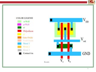
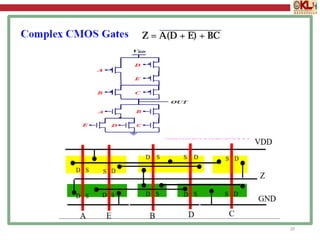
  • 23. 23 Optimized stick diagram layout of complex cmos logic gate
  • 24. 24
  • 25. 25
  • 26. 26
  • 27. 27
  • 28. 28
  • 29. 29
  • 30. 30
  • 31. 31
  • 32. 32
  • 33. 33
  • 34. 34
  • 36. 36 Sequential logic circuit is a logic circuit in which the output is determined by the current inputs as well as the previously applied input variables. A sequential circuit consisting of a combinational circuit and a memory block in the feedback loop .
  • 37. 37 The critical components of sequential systems are the basic regenerative circuits, which can be classified into three main groups: Bistable circuits, Monostable circuits, and Astable circuits. The general classification of non-regenerative and regenerative logic circuits is shown in Fig.
  • 38. 38 The basic bistable element consists of two identical cross-coupled inverter circuits as shown in figure:
  • 39. 39 Figure shows the circuit diagram of a CMOS two-inverter bistable element. At the unstable operating point of this circuit, all four transistors are in saturation, resulting in maximum loop gain for the circuit. If the initial operating condition is set at this point, any small voltage perturbation will cause significant changes in the operating modes of the transistors. Thus, we expect the output voltages of the two inverters to diverge and eventually settle at VOH and VOL, respectively.
  • 40. 40 If the set input (S) is equal to logic "1" and the reset input is equal to logic "0," then the output node Q will be forced to logic " 1 " while the output node Q is forced to logic "0." This means that the SR latch will be set, regardless of its previous state. Similarly, if S is equal to "0" and R is equal to " 1," then the output node Q will be forced to "0" while Q’ is forced to "1." Thus, with this input combination, the latch is reset, regardless of its previously held state. Finally, consider the case in which both of the inputs S and R are equal to logic “1 ." In this case, both output nodes will be forced to logic "0," which conflicts with the complementarily of Q and Q’. Therefore, this input combination is not permitted during normal operation and is considered to be a not allowed condition.
  • 41. 41
  • 42. 42
  • 43. 43 The operation of the CMOS SR latch circuit can be examined in more detail by considering the operating modes of the four nMOS transistors, MI, M2,M3, and M4. If the set input (S) is equal to VOH and the reset input (R) is equal to VOL,both of the parallel-connected transistors Ml and M2 will be on. Depletion-load nMOS SR latch circuit based on NOR2 gates.
  • 44. 44 SR Latch based on NAND Gate The small circles at the S and R input terminals represents that the circuit responds to active low input signals.
  • 45. 45 Truth table of CMOS SR latch using NAND gate if S is equal to "0”and R is equal to " 1," the output Q attains a logic " 1 " value and the complementary output Q becomes logic "0." Thus, in order to set the NAND SR latch, a logic "0" must be applied to the set (S) input. Similarly, in order to reset the latch, a logic "0" must be applied to the reset (R) input. The conclusion is that the NAND-based SR latch responds to active low input signals, as opposed to the NOR-based SR latch, which responds to active high inputs.
  • 46. 46
  • 48. 48 Clocked SR Latch The clock pulse will be assumed to be a periodic square waveform, which is applied simultaneously to all clocked logic gates in the system. Gate-level schematic of the clocked NOR- based SR latch.