![Design for Test [DFT]
• System on Chip (SOC): All the blocks like memory, ALU, RAM,ROM,
Microprocessor, Microcontroller etc are integrated on a chip is called
as SOC. It mainly consists of 4 blocks.](https://image.slidesharecdn.com/designfortestdft-11-231227151941-28a508a3/85/Design-for-Test-DFT-1-1-pdf-DESIGN-DFT-1-320.jpg)
![Design for Test [DFT]
• DFT: Generates the test patterns and those patterns are able to
detect any manufacturing defects.
• DFT engineers job is to facilitate the mechanism to identify the
defective parts & non defective parts.
• It provides interfacing between pre-manufacturing & post-
manufacturing.
DFT Engineers – Gives the Test vectors to the Test engineers.
Test Engineers – take the test vectors and applies to the chip,
specifies chip pass/fail.](https://image.slidesharecdn.com/designfortestdft-11-231227151941-28a508a3/85/Design-for-Test-DFT-1-1-pdf-DESIGN-DFT-2-320.jpg)


![Design for Test [DFT]-1 (1).pdf DESIGN DFT](https://image.slidesharecdn.com/designfortestdft-11-231227151941-28a508a3/85/Design-for-Test-DFT-1-1-pdf-DESIGN-DFT-10-320.jpg)
![Design for Test [DFT]-1 (1).pdf DESIGN DFT](https://image.slidesharecdn.com/designfortestdft-11-231227151941-28a508a3/85/Design-for-Test-DFT-1-1-pdf-DESIGN-DFT-11-320.jpg)


![Design for Test [DFT]-1 (1).pdf DESIGN DFT](https://image.slidesharecdn.com/designfortestdft-11-231227151941-28a508a3/85/Design-for-Test-DFT-1-1-pdf-DESIGN-DFT-19-320.jpg)


![Design for Test [DFT]-1 (1).pdf DESIGN DFT](https://image.slidesharecdn.com/designfortestdft-11-231227151941-28a508a3/85/Design-for-Test-DFT-1-1-pdf-DESIGN-DFT-36-320.jpg)


![Design for Test [DFT]-1 (1).pdf DESIGN DFT](https://image.slidesharecdn.com/designfortestdft-11-231227151941-28a508a3/85/Design-for-Test-DFT-1-1-pdf-DESIGN-DFT-97-320.jpg)
![Design for Test [DFT]-1 (1).pdf DESIGN DFT](https://image.slidesharecdn.com/designfortestdft-11-231227151941-28a508a3/85/Design-for-Test-DFT-1-1-pdf-DESIGN-DFT-98-320.jpg)


![Design for Test [DFT]-1 (1).pdf DESIGN DFT](https://image.slidesharecdn.com/designfortestdft-11-231227151941-28a508a3/85/Design-for-Test-DFT-1-1-pdf-DESIGN-DFT-101-320.jpg)
Design for Test [DFT]-1 (1).pdf DESIGN DFT
- 1. Design for Test [DFT] • System on Chip (SOC): All the blocks like memory, ALU, RAM,ROM, Microprocessor, Microcontroller etc are integrated on a chip is called as SOC. It mainly consists of 4 blocks.
- 2. Design for Test [DFT] • DFT: Generates the test patterns and those patterns are able to detect any manufacturing defects. • DFT engineers job is to facilitate the mechanism to identify the defective parts & non defective parts. • It provides interfacing between pre-manufacturing & post- manufacturing. DFT Engineers – Gives the Test vectors to the Test engineers. Test Engineers – take the test vectors and applies to the chip, specifies chip pass/fail.
- 3. Goal of DFT: Goal of DFT is to identifying the defects and separating the faulty parts. But not identifying where is the defect, how the defect occurs. • DFT Engineers provides i/p’s in the format of Test vectors to the Test Engineer team to apply on the manufactured IC and prove the IC’s pass/fail. • To test the Digital type logic, we use Scan method . • For I/O defects we use – BSCAN (Boundary Scan) • For memory – MBIST (Memory BIST) • For Analog – ADFT (Analog DFT) There is no Generic way to Test Analog (There is no fixed methodology to test Analog).
- 4. Design Structures: 1) Digital: (i) Combinational Logic (ii) Sequential Logic 2) Inputs & Outputs (I/O) 3) Memories 4) Analog
- 5. Inputs & Outputs: It takes input from the external input world and gives to the input pad, then to some internal logic and further sends the output to external world through output pad.
- 6. Bidirectional Pad: • It has a logic inside the chip, If oe=1, then pad works as an output pad. If oe=0, then pad works as an input pad, i.e., signal going into chip.
- 7. Tri - State Pad: When oe=1, the output goes to the external world. When oe=0, it creates an high impendence state, i.e., it completely block signals going to i/p (or) o/p.
- 8. DFT Role
- 9. IC Classification: S.no No of Transistors per Chip Technology name 1 Less than 100 SSI 2 100 – 10,000 MSI 3 10,000 – 1,00,000 LSI 4 Greater than 1,00,000 VLSI 5 Greater than 100 millions ULSI
- 12. • Library is a file, which we have all combinational and sequence elements. • If OR is there in netlist, tool won’t understand it, it will check in the library for OR gate, if it finds there then it will perform the corresponding operation. • Eg: OR2x4_LVT 2 – no of i/p’s X4 – Drive strength – capacity of the cell to drive the load. (Drive Strength means Fan-Out)number of gates that an output of a gate can drive.
- 13. Actually 3 types of library cells LVT (Low Threshold Voltage) RVT (Regular Threshold Voltage) or SVT (Standard Threshold Voltage) HVT (High Threshold Voltage) 1) Fast cell 2) High Leakage 1) Medium Cell 2) Medium Leakage 1) Slow Cell 2) Low Leakage
- 14. Cont.. • Suppose if we want to build a processor that works with higher speed in a Giga Hz, then we have to pick OR2 cell with LVT. • Similarly, if we want low power devices then pick OR2 with HVT. • If it is a Trade off then we go with RVT.
- 15. • Library means not only AND, OR, NOT, XOR, XNOR, it also has drive strength, and drive strength has different thresholds (LVT, RVT, HVT). Eg: AND2_X4_LVT RTL code Netlist • Maximum drive strength is 32,it will change depending upon technology • Tool reads the RTL, understands the functionality and it will converts into gates from the library and tries to implement same functionality coded in RTL. Synthesis Tool (Dc Compiler)
- 16. 1. RTL Functionality = netlist functionality. 2. It also do optimization (PPA) a) Power b)Performance c) Area i.e., Power Optimization go for HVT cell. Performance Optimization go for LVT cell. Area Optimization drive strength. (if drive strength is more, then more gates are there, then size (or) area increases) we prepare to take lower drive strength.
- 17. • Suppose, if we need 100MHz speed but with lesser area • Suppose, this will be done with X2 and X4, then tool picks X2 only. depending on design constraints given to the synthesis tool, it will generate a netlist. • Suppose, if we want the chip to work at 500MHz, we cannot get 500MHz from the entire design. Some blocks has 500MHz, some has 50MHz, 100MHz, 250MHz…. The tool will decide, whether to use LVT, HVT,RVT (or) combination of LVT and HVT depending on PPA (Power, Performance and Area). i.e., 20% of LVT, 60% of LVT + HVT, 20% HVT that will be decided by the tool depending on constraints.
- 18. ASIC FLOW • IC for a specific functionality, eg: mobile, laptop. • Same design is used to manufacture millions of products. • When we need higher volumes of IC’s we go by ASIC. FPGA: • It supports different applications( like adder, subtractor, multiplier..). i.e., Reconfigurable. • Whereas ASIC is application specific IC, i.e.,suppose an adder ASIC only performs Addition. • Suppose Adder is designed with ASIC & FPGA. • Then PPA is better in ASIC then FPGA. • ASIC performs only one application, whereas FPGA is reconfigurable hence extra circuit is needed for FPGA.
- 20. Defects in Silicon • IC manufacturing process is defect-prone. • Database given for manufacturing and outcome of a manufactured chip both are functionally equal. • I need to prove that, they are equal or not. If they are equal it is fault free otherwise , there is a defect or fault. • Defects during manufacturing open or short are caused by impurities, shorts for additive material, opens for subtraction material.
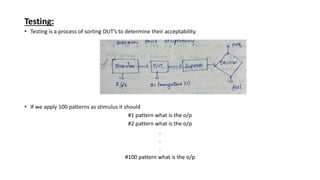
- 21. Testing: • Testing is a process of sorting DUT’s to determine their acceptability. • If we apply 100 patterns as stimulus it should #1 pattern what is the o/p #2 pattern what is the o/p . . . #100 pattern what is the o/p
- 22. • First we should have expected o/p’s • Then apply stimulus (I/P pattern) Suppose I/P O/P #1 1 #2 0 #3 . . 0 . . #100 1 I/P O/P #1 1 #2 0 #3 . . 0 . . #100 1 if any one pattern fails then it is a defective chip and it is separated.
- 23. Quality – Defective Parts Per Million (DPPM) Yield: • Suppose 100 IC’s are manufactured and all 100 IC’s are pass then we can say 100% “Yield”. • Suppose 90 IC’s are pass then we can say 90% yield; 10% is yield loss. Yield = • i.e., How many pass, after manufacturing is called “Yield” . DPPM: • Suppose 1 Million IC’s are shipped to the customer, after DFT, suppose 100 IC’s are returned back from the customer, then DPPM = 100. Note: Even after DFT, there may be possibility of chip fail. How many pass Total Manufactured
- 24. ATE (Automatic Test Equipment) • After manufacturing we are using ATE to test. TE (Test Engineer): • Work is writing test program, applying them; and during testing if the chips are failing, then he go back to DFT Engineer.
- 25. T6682 ATE Block Diagram
- 26. Multisite testing 1) One ATE tests several (usually identical) devices at the same time. 2) For both probe (wafer level testing) and package test(taking a die from wafer, and putting in a package). 3) DUT interface board has >1 sockets. 4) Add more instruments to ATE to handle multiple devices simultaneously. 5) Usually test 2 or 4 DUT’s at a time, usually test 32 or 64 memory chips at a time.
- 27. Cont… • Suppose, if we have 100 million IC’s, • Let us assume it will take 1min to test one IC, then to test 100 millions, it will take 100 million minutes. • Suppose, a mobile has 3 IC’s , for 100 million mobiles, it will take 30 million minutes. • Therefore, to increase the testing speed, instead of testing one IC, you can test 2 IC’s at a time is called Dual Site Testing • 4 IC’s at a time – Quad site testing. • 8 IC’s at a time – Octal site testing. , if we test 8 IC’s in a min then we need = 12 million minutes instead of 100 million minutes. 100 millions 8
- 28. ATE:
- 29. Cont…. • Here, ATE generates test pattern to the wafer, then failure dies are identified , by taking the information of fail dies from ATE, the wafer map will Ink the dies which are fail. • Now by using dicing and binning , here sorting is done, i.e., good parts (dies) are Dicing (cut and send to package) and bad (or) Ink dies are moved to Bin.
- 30. Manufacturing Test: 1) A speck of dust on a wafer is sufficient to kill chip. 2) Yield of any chip is <100%. Must test chips after manufacturing before delivering to customers to only ship good parts. 3) Manufacturing testers are very expensive a. Minimize time on tester b. Careful selection of test vectors.
- 31. What is DFT ? • It is a technique of adding testability features to IC design. • Developing and applying manufacturing tests. • The manufacturing tests help to separate defective components from the healthy ones. • Actually, let us assume an AND gate IC. • During the manufacturing , test logic also inserted. • Now apply test pattern to Test logic, to check the functionality of AND gate, After verification, if everything is ok then manufacturer disables the Test logic.
- 32. What are DFT Goals ? Quality: A high degree of confidence during testing Test cost reduction Time to volume reduction through test automation. Ad-Hoc DFT: To enhance a designs testability without major changes to the design style. Minimizing Redundant logic Minimizing Asynchronous logic Isolating clocks from the logic Adding internal control and observation points. However structured DFT techniques yields greater results.
- 33. Structured DFT: 1) More systematic and automatic approach. 2) Scan Design 3) BIST 4) Boundary Scan • Goal is to increase the Controllability & Observability of a circuit. • Actually by using Ad-Hoc DFT we cannot test each and every block but by using structured DFT we can test each and every block. like, to test digital logic – use Scan methodology to test memories – MBIST to test I/O’s - JTAG (or) Boundary Scan.
- 34. • Suppose, if we want to manufacture an AND gate, • Here 3 nodes are present, during manufacturing there are two possibilities 1) stuck at – 0; 2) stuck at – 1 • Each node has a possibility of 2 defects.
- 35. Therefore, a simple AND gate with 3 nodes has 6 possible defects.
- 37. • DFT helps to a) Verify chip’s functionality. b) Reduce debug time. c) Faster ramp to volume production. o/p: b & c.
- 38. Definitions: 1) Defects :Imperfection of flow that happen in a particular DUT. 2) Faults : A representation/modelling of that defect. 3) Failure: Non- Performance of the intended function of the device mainly due to the defect.
- 39. DFT Definitions: A Design is Testable: • All internal nodes of interest are simultaneously controllable ( to a desired logic value) and observable. Design for testability: • A methodology (or) a collection of methodologies, which results in the creation of a testable design. Diagnosis: • To locate the cause of misbehavior after the incorrect behavior is detected.
- 40. Functionality vs Structural ATPG:
- 41. Cont… , 13x2 =26 , for 64-bit, total no of faults = 26x64 = 1664 ,for 64-bit adder, we have 1664+640=2304 faults.
- 42. Functional vs Structural testing • If we go by functional way of testing • Functional ATPG – generate complete set of tests for circuit i/p – o/p combinations. 129 – i/p’s , 65 – o/p’s. , 2129 = 680,564,733,841,926,749,214,863,536,422,912 patterns. by using 1GHz ATE (High speed ATE), would take 2.15x10²² years. (which is not feasible).
- 43. Cont…. • Where as by structural test, No redundant adder hardware, 64 bit slices. Each with 36 faults (using fault equivalence) At most 64x36=2304 faults. By using 1GHz ATE – 0.000001728 sec (1.7μs). Industries prefer structural testing. suppose, with structural testing we got 99.5%. • For coverage of 0.5% go for functional testing. designers gives small set of functional tests – augment with structural tests to boost coverage to 98+%.
- 44. Design Environment Setup Link library Target library Search path Tool Invocation Netlist Constraints
- 45. Cont…
- 46. • Suppose, the tool does not find latch cell in link library then it shows error like Black Box (or) cell not found etc.. • Eg: I have 40nm synthesis, I want to convert this in 28nm netlist, to do Scan Insertion. i/p is 40nm netlist we need link library (read). Now o/p is 28nm netlist we need Target library (write). Link Library: • The tool uses the link lib to read i/p netlist (reading all the cells) (or) for each cell (like OR, AND , NOT, LATCH…) the tool will go and look into the link library.
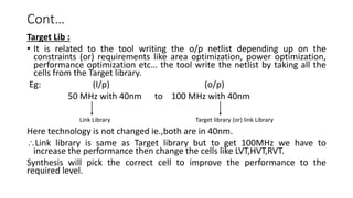
- 47. Cont… Target Lib : • It is related to the tool writing the o/p netlist depending up on the constraints (or) requirements like area optimization, power optimization, performance optimization etc… the tool write the netlist by taking all the cells from the Target library. Eg: (I/p) (o/p) 50 MHz with 40nm to 100 MHz with 40nm Here technology is not changed ie.,both are in 40nm. Link library is same as Target library but to get 100MHz we have to increase the performance then change the cells like LVT,HVT,RVT. Synthesis will pick the correct cell to improve the performance to the required level. Link Library Target library (or) link Library
- 48. • Eg: 100MHz with 40nm 100 MHz with 28nm Search Path: • It is the path where you will get all libraries and telling the tool where to look for Target lib. To read i/p link lib Technology is different Target lib is used to write the o/p netlist
- 49. Single Struck-at fault: • Only 1 node is faulty in the entire design at one point of time, it is permanently S@0 (or) S@1. it does not toggle. • The fault can be either at i/p (or) o/p of a gate.
- 50. Testability:
- 51. • Here, observability failure is gone, because , we can put 1/0 at that node and that 1/0 can be transferred to PO(Primary O/p). • Similarly Controllability failure is gone, because we can put 0 at PI (Primary Input) and by setting Test_mode =1 then we can get 0 at o/p of MUX ( at any node we can put 1/0) If Test_mode=0 then we are enabling the OR gate (functional logic) through OR gate take place. If Test_mode=1, then we are disabling the OR gate. here for one OR gate, we have used, 1 Mux ,1 PO,1 PI. • Suppose for 100 OR gates we have to consider 100 Mux, 100 PI, 100 Po. • Theoretically, it solves the problem but practically it is not possible to take “n” no. of i/p’s.
- 52. (i) Controllability: The ability to set a node in a design to a desired state, i.e., logic 0 (or) 1. (ii) Observability: The ability to observe a change (valid o/p) in logic value of a node in a design. (iii) Testability: If a design is well-controllable & observable it is said to be easily testable. (iv) Not possible to add such directly controllable & observable points to every gates in an actual design.
- 53. To avoid this, scan design comes. (to avoid using PI & PO). Actually any digital path you take it will fall under 4 paths. i.e., I. I/p – Reg II. Reg - Reg III. Reg – O/p IV. I/p – O/p
- 54. Cont…. • But how can we test the combination circuit which is inside the chip, i.e., combinational circuit sitting between I/P and Reg (f/f) (or) between Reg to Reg (or) between Reg to O/p.
- 55. Cont… • At this station , we use virtual i/p from the reg and virtual o/p from the reg. • That means we have to use Scan Design, to controllability & observability of the logic sitting internally in the chip.
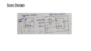
- 56. Scan Design
- 57. Cont… • We cannot access the D-ff , which is internally sitting in the chip. So we placed a 2:1 MUX before a D-ff during manufacturing. If scan_en =0, then normal D-ff operation takes place (functional data transferred into the D-ff it is called functional path). If scan_en =1, then scan_data (either 1/0) is transferred to D-ff by applying sys_clk that 1/0 is stored in D-ff, we can access through Q. by doing this controllability & observability are there.
- 58. Cont…. Before scan insertion After scan insertion
- 59. Scan Operation
- 60. Scan Operation: 1) Select shift mode, SE=1. 2) Shift-in/load scan cell values. 3) Select capture mode, SE=0. 4) Apply/force primary i/p’s. 5) Measure primary o/p’s. 6) Capture combinational logic response into scan flops. 7) Select shift mode, SE=1. 8) Shift-out / unload the scan cells data. 9) Shift-in the next scan pattern. Process repeats again and again.
- 61. Scan chain operation for stuck at Test:
- 62. Scan Test Time: • Suppose , If we have 1000 flops.
- 63. Cont… • The optimization is, during 1st pattern shift out we require 1000 pulses, at the time of shifting suppose if we use 2nd pattern at scan in for shift in (load) and 1st pattern shift out are taken care by only 1000 pulses. • In this way we can reduce the Test clock cycles (or) Test time. Most of the clock cycles are consumed by shift in & shift out. • Shift in & shift out are depends on scan chain length. , if we are having shorter chains then Test time will be reduced.
- 64. Scan Benefits: 1) Makes the complete design look like a shift register. 2) Scan enables us to get data in (to the design) and data out (of the design) easily. 3) Easy test pattern generation for design. 4) Basis for many ATPG related tools. • Which comes first in the SoC flow? a. ATPG b. Pattern simulation c. Scan Insertion d. Pattern Conversion Ans:c,a,b,d.
- 65. Scan Models • Most commonly used scan models are: MUX-DFF Clocked Scan LSSD (Level Sensitive Scan Design) (Latch based)
- 66. Clocked Scan • Actually clk itself consumes more power • Here we are using another clk i.e., SC_Clk, increases the complexity and power requirements. • Uses dedicated test clk (SC-CLK) in addition to sys_clk. • Operation: Functional mode: Data, sys_clk Test mode: SC_IN, SC_CLK • Need to route an extra clock tree.
- 67. LSSD: • Uses 2 test clocks: Aclk, Bclk. • Operation: Functional mode: data, sys_clk. Test mode: sc_in, Aclk, Bclk. • Need to route an extra clock tree. • Additional area due to extra location.
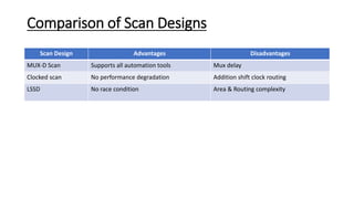
- 68. Comparison of Scan Designs Scan Design Advantages Disadvantages MUX-D Scan Supports all automation tools Mux delay Clocked scan No performance degradation Addition shift clock routing LSSD No race condition Area & Routing complexity
- 69. Scan Operation Clock Any signal that can change the state of flipflop (or) Reg is called clk. (set (or) reset are also called clock).
- 70. Scan Golden Rules (or) DRC’s: All DRC’s are netlist based. DFT rule 1: • All the internal clocks must be controlled by port level clock signal (primary i/p) in scan test mode. • The internal pin Q may be 1 or 0. hence we cannot control the clock of FF2. • Actually all the internal clocks must be controlled by the port level clk, for this to happen, a mux is placed, this mux should not effect the functionality (i.e: Q to clock connection).
- 71. DFT Rule: 2 • Avoid implementation of combinational feedback circuit. If present, the feedback loop will be broken to test. • The feedback signal may not be testable (observable) in test mode.
- 72. DFT Rule: 3 • Asynchronous SET/RESET pins of flipflops must be controlled by a port level RESET (primary i/p) in Scan Test mode.
- 73. DFT Rule: 4 • Gated clock must be enabled in scan test mode. • Whenever clk is applied at port level, that will reach as i/p to AND gate; if 2nd i/p to the AND gate is ‘1’ then clk will be propagated; if 2nd i/p is ‘0’ then clock won’t propagate.
- 74. Cont…
- 75. Cont: • If the Testmode=1, o/p of AND is 0, then latch will store this ‘0’ and at o/p of latch it is ‘1’. , clk is propagated, (we need D=0 always). • But here there is no controllability of Hold. i.e: if the Hold receives the i/p from any combo logic then additional scan flop is needed to observe the value. • If the Hold receives i/p from any scan flop then the additional scan flop is not needed for observability of Hold value.
- 76. DFT Rule: 5 • Latches have to be avoided as much as possible, if present, make it transparent in scan test mode. • In an Edge- triggered design, it is difficult to put latches on a scan chain because the library does not contain their edge- triggered scan equivalents. • If they (latch) are not part of a scan chain, their o/p’s will be difficult to control. The faults coverage will therefore be very low.
- 77. DFT Rule: 6 • Do not replace flipflops of the shift register structure by equivalent scan flops. • i.e., suppose , if we are not having combinational logic to test, then no need of scan flops. • Similarly, if we are having shift registers in a functional block, and there is no combo logic in the functional block, then there is no need to convert the flipflops of shift registers to scan chain.
- 78. • Similarly if there is a combo logic, and a 32-bit shift reg in the functional block, then we need to change only one (first) flop in the shift reg to scan flop. • Then to test combo logic, only 0th flop needs to convert as scan flop and remaining 31 flops will remain as normal shift-reg. • For efficient area purpose, the flipflops of the shift register structure will not be replaced by equivalent scan flipflops. • Compare to normal flops, scan flops takes more area.
- 79. DFT Rule: 7 • Clock should not be used as data in scan test mode. • If Testmode =1; then o/p of OR is 1. • Now, i/p to AND is 1 and another i/p is from Data, • if data =10101, then that data will be stored in MUX Scan flop.
- 80. DFT Rule: 8 • By pass the memory in scan test mode. All the paths ending at memory cell are not observable. All the paths starting from memory are not controllable.
- 81. Suppose, a combo logic is present like this, • The o/p of the combo logic is hitting the memory, if the ,memory is present in the functional design then it is like dead end, we cannot observe the value. for observability we bypasses to mux through a flop. • Similarly, the o/p from memory is also not controllable. • In the bottom, a combo logic is present, for observability a flop is placed.
- 82. DFT Rule: 9 The scan enable signal must be buffered adequately. 1) The scan enable signal that causes all flip flops in the design to be connected to form the scan shift register, has to be fed to all flip flops in the design. This signal will be heavily loaded. 2) The problem of buffering this signal is identical to that of clock buffering. 3) The drive strength of scan enable port on each block of the design must be set to a realistic value when the design is synthesized. 4) If this port is left unconstrained during synthesis, it could result in silicon failure.
- 83. DFT Rule: 10 • Avoid multicycle paths as much as possible . (Ideally Zero)
- 84. DFT Rule: 11 • Negative edge flops should be placed in the start of the scan chain.
- 85. See in previous figure for 4 clk pulses, the value loaded is 1101 but not 1010. this is because –ve edge flops are taken in the middle. Those must be at the beginning.
- 86. Scan Types 1) Full scan 2) Partial scan 3) Partition scan
- 87. (1)Full Scan: Full scan is a scan design methodology that replaces all memory elements in the design with their scan-able equivalents and then stitches them into scan chains. Benefits: 1) Highly –automated process(tool generates less pattern for best coverage) 2) Highly – effective, predictable method. 3) Easy to use. 4) Assured quality.
- 88. (2) Partial Scan: Full scan design makes all storage elements scannable, it may not be acceptable for all your designs because of area and timing constraints. Where as partial scan is a scan design methodology only a percentage of the storage elements in the design are replaced by their scannable equivalents and stitched into scan chains. Benefits: 1) Reduce impact in area 2) Reduced impact on timing 3) More flexibility between overhead and fault coverage.
- 89. Full vs Partial Scan
- 90. (3) Partition scan: • It is for complex SoC designs. • The ATPG process on very large, complex designs can often be unpredictable. • Large designs which are split into a no. of design blocks. Benefits : 1) Improves test coverage and runtime. 2) Less power consuming since each block tested separately.
- 91. How to fix below DRC issue? • We cannot control the clk, because o/p from combo logic is ‘0’ then the clk won’t propagate to the flop. So o/p of combo logic maybe 0 (or) 1. the clk should be from top level only. we modify this circuit.
- 92. • Combinational Feedback loop? • We cannot observe the o/p Q because it keeps on changing for observability we have to break that loop by placing OR gate.
- 93. Lockup Latches • Block A is following the guidelines (placing –ve edge clk at first place) similarly Block B also following the guidelines. • But when both blocks are combined then they violated the rule, at this situation lockup latches are used.
- 94. • Even though we are giving clk pulses to all the flops, there is a clock skew (i.e., expected-arrival) i.e., the 1st flop receives clk first, and further flop receives last because of this,clk skew is present, at this situation lockup latch is introduced. • The lockup latch is active low enable, • It holds the data for half cycle. • In the industries, lockup latches are inserted at the end of the every scan chain within the block itself.
- 95. Clock Gating: • A latch is placed, to reduce the glitches. • En(enable) acts as data pin, here clk is –ve edge (or) –ve level triggered. • The target is to get neat gated clk at o/p. • A latch with a gate is called ICG (Integrated Clock Gate) it comes as one macro cell. i.e., It is not like one latch and one separate AND gate combined.
- 99. Now we know if clk2 is coming early than clk1 then data loaded correctly, what if we inserted a lockup latch here,
- 100. • When two clk domains are combinely used in a chain then we cannot see which clk is coming first and which one is second. • If clk2 comes 1st than clk1 then no issues, if clk1 comes 1st than clk2 then there is issue. • So, at that situation lockup latches are used , to load the data correctly.