


![A detailed analysis of the borrowing process for this example, indicating first a bor-
row of 1 from column 1 and then a borrow of 1 from column 2, is as follows:
205 18 [2 102
0 101
5 100
]
[ 1 101
8 100
]
note borrow from column 1
[2 102
(0 1) 101
(10 5) 100
]
[ 1 101
8 100
]
note borrow from column 2
[(2 1) 102
(10 0 1) 101
15 100
]
[ 1 101
8 100
]
[1 102
8 101
7 100
] 187
The analysis of borrowing for binary subtraction is exactly the same, except that we
work with powers of 2 instead of powers of 10.Thus for a binary number, borrowing 1
from column n is equivalent to subtracting 1 from column n and adding 2 (102) to col-
umn n 1.The value of the binary number is unchanged because 1 2n
2 2n1
.
A detailed analysis of binary subtraction example (c) follows. Starting with the
rightmost column, 1 1 0. To subtract in the second column, we must borrow
from the third column. Rather than borrow immediately, we place a 1 over the third
column to indicate that a borrow is necessary, and we will actually do the borrowing
when we get to the third column. (This is similar to the way borrow signals might
propagate in a computer.) Now because we have borrowed 1, the second column
becomes 10, and 10 1 1. In order to borrow 1 from the third column, we must
borrow 1 from the fourth column (indicated by placing a 1 over column 4). Column
3 then becomes 10, subtracting off the borrow yields 1, and 1 0 1. Now in col-
umn 4, we subtract off the borrow leaving 0. In order to complete the subtraction,
we must borrow from column 5, which gives 10 in column 4, and 10 1 1.
The multiplication table for binary numbers is
0 0 0
0 1 0
1 0 0
1 1 1
The following example illustrates multiplication of 1310 by 1110 in binary:
1101
1011
1101
1101
0000
1101
10001111 14310
14 Unit 1
↓
↓ ↓
↓](https://image.slidesharecdn.com/fundamentalsoflogicdesign6thcharlesh-240226091353-b43ce575/85/Fundamentals-of-Logic-Design-6th-Charles-H-Roth-pdf-37-320.jpg)


![Again, note that the overflow in case 6 is easy to detect because the addition of two
negative numbers yields a positive result.
The proof that the end-round carry method gives the correct result follows for
cases 4 and 5:
Case 4: A B (where B A)
B (2n
1 A) B 2n
(B A) 1
The end-around carry is equivalent to subtracting 2n
and adding 1, so the result is
(B A), which is correct.
Case 5: A B (A B 2n1
)
(2n
1 A) (2n
1 B) 2n
[2n
1 (A B)] 1
After the end-around carry, the result is 2n
1 which is the
correct representation for (A B).
The following examples illustrate the addition of 1’s and 2’s complement num-
bers for a word length of n 8:
1. Add 11 and 20 in 1’s complement.
11 00001011 20 00010100
taking the bit-by-bit complement,
11 is represented by 11110100 and 20 by 11101011
11110100 (11)
11101011 (20)
(1) 11011111
1 (end-around carry)
11100000 31
2. Add 8 and 19 in 2’s complement
8 00001000
complementing all bits to the left of the first 1, 8, is represented by 11111000
11111000 (8)
00010011 19
00001011 11
(discard last carry)
Note that in both cases, the addition produced a carry out of the furthest left
bit position, but there is no overflow because the answer can be correctly
←
(1)
I⎯⎯→
(A B)
(A B)
B
A
A
20 Unit 1](https://image.slidesharecdn.com/fundamentalsoflogicdesign6thcharlesh-240226091353-b43ce575/85/Fundamentals-of-Logic-Design-6th-Charles-H-Roth-pdf-43-320.jpg)


![Number Systems and Conversion 23
ASCII Code ASCII Code ASCII Code
Character A6 A5 A4 A3 A2 A1 A0 Character A6 A5 A4 A3 A2 A1 A0 Character A6 A5 A4 A3 A2 A1 A0
space 0 1 0 0 0 0 0 @ 1 0 0 0 0 0 0 ‘ 1 1 0 0 0 0 0
! 0 1 0 0 0 0 1 A 1 0 0 0 0 0 1 a 1 1 0 0 0 0 1
“ 0 1 0 0 0 1 0 B 1 0 0 0 0 1 0 b 1 1 0 0 0 1 0
# 0 1 0 0 0 1 1 C 1 0 0 0 0 1 1 c 1 1 0 0 0 1 1
$ 0 1 0 0 1 0 0 D 1 0 0 0 1 0 0 d 1 1 0 0 1 0 0
% 0 1 0 0 1 0 1 E 1 0 0 0 1 0 1 e 1 1 0 0 1 0 1
0 1 0 0 1 1 0 F 1 0 0 0 1 1 0 f 1 1 0 0 1 1 0
0 1 0 0 1 1 1 G 1 0 0 0 1 1 1 g 1 1 0 0 1 1 1
( 0 1 0 1 0 0 0 H 1 0 0 1 0 0 0 h 1 1 0 1 0 0 0
) 0 1 0 1 0 0 1 I 1 0 0 1 0 0 1 i 1 1 0 1 0 0 1
* 0 1 0 1 0 1 0 J 1 0 0 1 0 1 0 j 1 1 0 1 0 1 0
0 1 0 1 0 1 1 K 1 0 0 1 0 1 1 k 1 1 0 1 0 1 1
, 0 1 0 1 1 0 0 L 1 0 0 1 1 0 0 l 1 1 0 1 1 0 0
0 1 0 1 1 0 1 M 1 0 0 1 1 0 1 m 1 1 0 1 1 0 1
. 0 1 0 1 1 1 0 N 1 0 0 1 1 1 0 n 1 1 0 1 1 1 0
/ 0 1 0 1 1 1 1 O 1 0 0 1 1 1 1 o 1 1 0 1 1 1 1
0 0 1 1 0 0 0 0 P 1 0 1 0 0 0 0 p 1 1 1 0 0 0 0
1 0 1 1 0 0 0 1 Q 1 0 1 0 0 0 1 q 1 1 1 0 0 0 1
2 0 1 1 0 0 1 0 R 1 0 1 0 0 1 0 r 1 1 1 0 0 1 0
3 0 1 1 0 0 1 1 S 1 0 1 0 0 1 1 s 1 1 1 0 0 1 1
4 0 1 1 0 1 0 0 T 1 0 1 0 1 0 0 t 1 1 1 0 1 0 0
5 0 1 1 0 1 0 1 U 1 0 1 0 1 0 1 u 1 1 1 0 1 0 1
6 0 1 1 0 1 1 0 V 1 0 1 0 1 1 0 v 1 1 1 0 1 1 0
7 0 1 1 0 1 1 1 W 1 0 1 0 1 1 1 w 1 1 1 0 1 1 1
8 0 1 1 1 0 0 0 X 1 0 1 1 0 0 0 x 1 1 1 1 0 0 0
9 0 1 1 1 0 0 1 Y 1 0 1 1 0 0 1 y 1 1 1 1 0 0 1
: 0 1 1 1 0 1 0 Z 1 0 1 1 0 1 0 z 1 1 1 1 0 1 0
; 0 1 1 1 0 1 1 [ 1 0 1 1 0 1 1 { 1 1 1 1 0 1 1
0 1 1 1 1 0 0 1 0 1 1 1 0 0 ⏐ 1 1 1 1 1 0 0
0 1 1 1 1 0 1 ] 1 0 1 1 1 0 1 } 1 1 1 1 1 0 1
0 1 1 1 1 1 0 ^ 1 0 1 1 1 1 0 ~ 1 1 1 1 1 1 0
? 0 1 1 1 1 1 1 — 1 0 1 1 1 1 1 delete 1 1 1 1 1 1 1
TABLE 1-3 ASCII Code
Problems
1.1 Convert to hexadecimal and then to binary:
(a) 757.2510 (b) 123.1710 (c) 356.8910 (d) 1063.510
1.2 Convert to octal. Convert to hexadecimal. Then convert both of your answers to
decimal, and verify that they are the same.
(a) 111010110001.0112 (b) 10110011101.112](https://image.slidesharecdn.com/fundamentalsoflogicdesign6thcharlesh-240226091353-b43ce575/85/Fundamentals-of-Logic-Design-6th-Charles-H-Roth-pdf-46-320.jpg)


![3. Study Section 2.3, Boolean Expressions and Truth Tables.
(a) How many variables does the following expression contain?
How many literals?
A′BC′D AB B′CD D′
(b) For the following circuit, if A B 0 and C D E 1, indicate the out-
put of each gate (0 or 1) on the circuit diagram:
C
D
B
E
F
A
+
+
(c) Derive a Boolean expression for the circuit output.Then substitute A B 0
and C D E 1 into your expression and verify that the value of F
obtained in this way is the same as that obtained on the circuit diagram in (b).
(d) Write an expression for the output of the following circuit and complete
the truth table:
A
F =
B
F
A B A A B (A B)
A B C B AB C(AB )
(e) When filling in the combinations of values for the variables on the left side
of a truth table, always list the combinations of 0’s and 1’s in binary order.
For example, for a three-variable truth table, the first row should be 000,
the next row 001, then 010, 011, 100, 101, 110, and 111.Write an expression
for the output of the following circuit and complete the truth table:
B
C
A
F =
F
+
(f) Draw a gate circuit which has an output
Z [BC′ F(E AD′)]′
(Hint: Start with the innermost parentheses and draw the circuit for AD′ first.)
Boolean Algebra 29](https://image.slidesharecdn.com/fundamentalsoflogicdesign6thcharlesh-240226091353-b43ce575/85/Fundamentals-of-Logic-Design-6th-Charles-H-Roth-pdf-52-320.jpg)
![30 Unit 2
4. Study Section 2.4, Basic Theorems.
(a) Prove each of the Theorems (2-4) through (2-8D) by showing that it is
valid for both X 0 and X 1.
(b) Determine the output of each of these gates:
A
A
A
A
A′
A
A′
A
A
0
A
A
1
0 1
A
+ + + +
(c) State which of the basic theorems was used in simplifying each of the fol-
lowing expressions:
(AB′ C) 0 0 A(B C′) 1 1
(BC′ A)(BC′ A) BC′ A X(Y′ Z) [X(Y′ Z)]′ 1
(X′ YZ)(X′ YZ)′ 0 D′(E′ F) D′(E′ F) D′(E′ F)
5. Study Section 2.5, Commutative, Associative, and Distributive Laws.
(a) State the associative law for OR.
(b) State the commutative law for AND.
(c) Simplify the following circuit by using the associative laws. Your answer
should require only two gates.
A
B
C
D
E
F
G
+
+
(d) For each gate determine the value of the unspecified input(s):
1
1
1
0 0 1 1
0
0
0
+ +
(e) Using a truth table, verify the distributive law, Equation (2-11).](https://image.slidesharecdn.com/fundamentalsoflogicdesign6thcharlesh-240226091353-b43ce575/85/Fundamentals-of-Logic-Design-6th-Charles-H-Roth-pdf-53-320.jpg)


![Boolean Algebra 33
(b) (A C′)(B′ D)(C′ D′)(C D)E
As usual, when we say multiply out, we do not mean to multiply out by brute
force, but rather to use the second distributive law whenever you can to cut
down on the amount of work required.
The answer to (a) should be of the following form:XX XX XX and (b) of the
form: XXX XXXXX, where each X represents a single variable or its complement.
Now factor your answer to (a) to see that you can get back the original
expression.
9. Study Section 2.8, DeMorgan’s Laws.
10. Find the complement of each of the following expressions as indicated. In your
answer, the complement operation should be applied only to single variables.
(a) (ab′c′)′
(b) (a′ b c d′)′
(c) (a′ bc)′
(d) (a′b′ cd)′
(e) [a(b′ c′d)]′
11. Because (X′)′ X, if you complement each of your answers to 10, you should
get back the original expression. Verify that this is true.
(a)
(b)
(c)
(d)
(e)
12. Given that F a′b b′c, F′
Complete the following truth table and verify that your answer is correct:
a b c a b b c a b b c (a b ) (b c ) F
0 0 0
0 0 1
0 1 0
0 1 1
1 0 0
1 0 1
1 1 0
1 1 1](https://image.slidesharecdn.com/fundamentalsoflogicdesign6thcharlesh-240226091353-b43ce575/85/Fundamentals-of-Logic-Design-6th-Charles-H-Roth-pdf-56-320.jpg)
![34 Unit 2
13. A fully simplified expression should have nothing complemented except the
individual variables. For example, F (X Y)′(W Z) is not a minimum prod-
uct of sums. Find the minimum product of sums for F.
14. Work Problems 2.8 and 2.9.
15. Find the dual of (M N′)P′.
16. Review the first 12 laws and theorems on page 55. Make sure that you can recog-
nize when to apply them even if an expression has been substituted for a variable.
17. Reread the objectives of this unit. If you are satisfied that you can meet these
objectives, take the readiness test.
[Note: You will be provided with a copy of the theorem sheet (page 55)
when you take the readiness test this time. However, by the end of Unit 3,
you should know all the theorems by memory.]
Boolean Algebra
2.1 Introduction
The basic mathematics needed for the study of the logic design of digital systems
is Boolean algebra. Boolean algebra has many other applications including set the-
ory and mathematical logic, but we will restrict ourselves to its application to
switching circuits in this text. Because all of the switching devices which we will use
are essentially two-state devices (such as a transistor with high or low output volt-
age), we will study the special case of Boolean algebra in which all of the variables
assume only one of two values. This two-valued Boolean algebra is often referred
to as switching algebra. George Boole developed Boolean algebra in 1847 and used](https://image.slidesharecdn.com/fundamentalsoflogicdesign6thcharlesh-240226091353-b43ce575/85/Fundamentals-of-Logic-Design-6th-Charles-H-Roth-pdf-57-320.jpg)


![Boolean Algebra 37
Next consider a circuit composed of two switches in parallel.
In this case, we have a closed circuit between terminals 1 and 2 iff switch A is closed
or switch B is closed. Using the same convention for defining variables as above, an
equation which describes the behavior of this circuit is
T A B
Thus, switches in a series perform the AND operation and switches in parallel per-
form the OR operation.
2.3 Boolean Expressions and Truth Tables
Boolean expressions are formed by application of the basic operations to one or
more variables or constants.The simplest expressions consist of a single constant or
variable, such as 0, X, or Y′. More complicated expressions are formed by combining
two or more other expressions using AND or OR, or by complementing another
expression. Examples of expressions are
AB′ C (2-1)
[A(C D)]′ BE (2-2)
Parentheses are added as needed to specify the order in which the operations are
performed. When parentheses are omitted, complementation is performed first fol-
lowed by AND and then OR. Thus in Expression (2-1), B′ is formed first, then AB′,
and finally AB′ C.
Each expression corresponds directly to a circuit of logic gates. Figure 2-1 gives
the circuits for Expressions (2-1) and (2-2).
A
B
1 2
A
A
B BE
E
AB′
(AB′ + C)
(C + D)
A(C + D) [A(C + D)]′
[A(C + D)]′ + BE
(a)
(b)
C
B
C
D
B′
+
+
+
FIGURE 2-1
Circuits for
Expressions (2-1)
and (2-2)](https://image.slidesharecdn.com/fundamentalsoflogicdesign6thcharlesh-240226091353-b43ce575/85/Fundamentals-of-Logic-Design-6th-Charles-H-Roth-pdf-60-320.jpg)
![38 Unit 2
An expression is evaluated by substituting a value of 0 or 1 for each variable. If
A B C 1 and D E 0, the value of Expression (2-2) is
[A(C D)]′ BE [1(1 0)]′ 1 0 [1(1)]′ 0 0 0 0
Each appearance of a variable or its complement in an expression will be referred
to as a literal. Thus, the following expression, which has three variables, has 10 literals:
ab′c a′b a′bc′ b′c′
When an expression is realized using logic gates, each literal in the expression cor-
responds to a gate input.
A truth table (also called a table of combinations) specifies the values of a
Boolean expression for every possible combination of values of the variables in the
expression. The name truth table comes from a similar table which is used in sym-
bolic logic to list the truth or falsity of a statement under all possible conditions.We
can use a truth table to specify the output values for a circuit of logic gates in
terms of the values of the input variables. The output of the circuit in Figure 2-2(a)
is F A′ B. Figure 2-2(b) shows a truth table which specifies the output of the
circuit for all possible combinations of values of the inputs A and B. The first two
columns list the four combinations of values of A and B, and the next column gives
the corresponding values of A′.The last column, which gives the values of A′ B, is
formed by ORing together corresponding values of A′ and B in each row.
+
A
B
F = A' + B
A'
(a)
FIGURE 2-2
Two-Input Circuit
and Truth Table
A B A F A B
0 0 1 1
0 1 1 1
1 0 0 0
1 1 0 1
A B C B AB AB C A C B C (A C)(B C)
0 0 0 1 0 0 0 1 0
0 0 1 1 0 1 1 1 1
0 1 0 0 0 0 0 0 0
0 1 1 0 0 1 1 1 1
1 0 0 1 1 1 1 1 1
1 0 1 1 1 1 1 1 1
1 1 0 0 0 0 1 0 0
1 1 1 0 0 1 1 1 1
TABLE 2-1
(b)
Next,we will use a truth table to specify the value of Expression (2-1) for all possible
combinations of values of the variables A, B, and C. On the left side of Table 2-1, we list
the values of the variables A, B, and C. Because each of the three variables can assume
the value 0 or 1, there are 2 2 2 8 combinations of values of the variables.These
combinations are easily obtained by listing the binary numbers 000, 001, . . . , 111. In the
next three columns of the truth table, we compute B′, AB′, and AB′ C, respectively.
Two expressions are equal if they have the same value for every possible com-
bination of the variables. The expression (A C)(B′ C) is evaluated using the
last three columns of Table 2-1. Because it has the same value as AB′ C for all
eight combinations of values of the variables A, B, and C, we conclude](https://image.slidesharecdn.com/fundamentalsoflogicdesign6thcharlesh-240226091353-b43ce575/85/Fundamentals-of-Logic-Design-6th-Charles-H-Roth-pdf-61-320.jpg)


![44 Unit 2
Simplify Z [A B′C D EF] [A B′C (D EF)′]
Example 2
Substituting: Z [ X Y ] [ X Y′ ]
Then, by (2-12D), the expression reduces to
Z X A B′C
Simplify Z = (AB C) (B′D C′E′) (AB C)′
Example 3
Substituting: Z Y′ X Y
By, (2-14D): Z X Y B′D C′E′ (AB C)′
Note that in this example we let Y (AB C)′ rather than (AB C) in order to
match the form of (2-14D).
2.7 Multiplying Out and Factoring
The two distributive laws are used to multiply out an expression to obtain a sum-
of-products (SOP) form.An expression is said to be in sum-of-products form when
all products are the products of single variables. This form is the end result when
an expression is fully multiplied out. It is usually easy to recognize a sum-of-prod-
ucts expression because it consists of a sum of product terms:
AB′ CD′E AC′E′ (2-15)
However, in degenerate cases, one or more of the product terms may consist of a
single variable. For example,
ABC′ DEFG H (2-16)
and
A B′ C D′E (2-17)
are still considered to be in sum-of-products form. The expression
(A B)CD EF
is not in sum-of-products form because the A B term enters into a product but is
not a single variable.
When multiplying out an expression, apply the second distributive law first when
possible. For example, to multiply out (A BC)(A D E) let
X A, Y BC, Z D E
¸˝˛ ¸˝˛ ¸˝˛
¸˝˛ ¸˝˛ ¸˝˛ ¸˝˛](https://image.slidesharecdn.com/fundamentalsoflogicdesign6thcharlesh-240226091353-b43ce575/85/Fundamentals-of-Logic-Design-6th-Charles-H-Roth-pdf-67-320.jpg)


![Boolean Algebra 47
2.8 DeMorgan’s Laws
The inverse or complement of any Boolean expression can easily be found by suc-
cessively applying the following theorems, which are frequently referred to as
DeMorgan’s laws:
(X Y)′ X′ Y′ (2-21)
(XY)′ X′ Y′ (2-22)
We will verify these laws using a truth table:
X Y X′ Y′ X Y (X Y)′ X′ Y′ XY (XY)′ X′ Y′
0 0 1 1 0 1 1 0 1 1
0 1 1 0 1 0 0 0 1 1
1 0 0 1 1 0 0 0 1 1
1 1 0 0 1 0 0 1 0 0
DeMorgan’s laws are easily generalized to n variables:
(X1 X2 X3 . . . Xn)′ X1′ X2′ X3′ . . . Xn′ (2-23)
(X1X2X3 . . . Xn)′ X1′ X2′ X3′ . . . Xn′ (2-24)
For example, for n 3,
(X1 X2 X3)′ (X1 X2)′X3′ X1′X2′X3′
Referring to the OR operation as the logical sum and the AND operation as logical
product, DeMorgan’s laws can be stated as
The complement of the product is the sum of the complements.
The complement of the sum is the product of the complements.
To form the complement of an expression containing both OR and AND opera-
tions, DeMorgan’s laws are applied alternately.
To find the complement of (A′ B)C′, first apply (2-22) and then (2-21).
Example 1
[(A′ B)C′]′ (A′ B)′ (C′)′ AB′ C
[(AB′ C)D′ E]′ [(AB′ C)D′]′E′ (by (2-21))
Example 2 [(AB′ C)′ D]E′ (by (2-22))
[(AB′)′C′ D]E′ (by (2-21))
[(A′ B)C′ D]E′ (by (2-22)) (2-25)
Note that in the final expressions, the complement operation is applied only to sin-
gle variables.](https://image.slidesharecdn.com/fundamentalsoflogicdesign6thcharlesh-240226091353-b43ce575/85/Fundamentals-of-Logic-Design-6th-Charles-H-Roth-pdf-70-320.jpg)

![Boolean Algebra 49
2.5 Multiply out and simplify to obtain a sum of products:
(a) (A B)(C B)(D′ B)(ACD′ E)
(b) (A′ B C′)(A′ C′ D)(B′ D′)
2.6 Factor each of the following expressions to obtain a product of sums:
(a) AB C′D′ (b) WX WY′X ZYX
(c) A′BC EF DEF′ (d) XYZ W′Z XQ′Z
(e) ACD′ C′D′ A′C (f) A BC DE
(The answer to (f) should be the product of four terms, each a sum of three variables.)
2.7 Draw a circuit that uses only one AND gate and one OR gate to realize each of the
following functions:
(a) (A B C D)(A B C E)(A B C F)
(b) WXYZ VXYZ UXYZ
2.8 Simplify the following expressions to a minimum sum of products.
(a) [(AB)′ C′D]′ (b) [A B(C′ D)]′ (c) ((A B′)C)′(A B)(C A)′
2.9 Find F and G and simplify:
A
A
T
T
G
P
F
B
R
T
R
S
S
(a)
(b)
+
+
+
+
+
A
B
A
B
B
B
A
A
Y
E F
D
B
C
1
(a)
(b)
+
+
+
+
+
+](https://image.slidesharecdn.com/fundamentalsoflogicdesign6thcharlesh-240226091353-b43ce575/85/Fundamentals-of-Logic-Design-6th-Charles-H-Roth-pdf-72-320.jpg)
 (f) A′ (B C)(D′E F)′ (D′E F)
2.12 Simplify each of the following expressions by applying one of the theorems. State
the theorem used.
(a) (X Y′Z) (X Y′Z)′
(b) [W X′(Y Z)][W′ X′(Y Z)]
(c) (V′W UX)′(UX Y Z V′W)
(d) (UV′ W′X)(UV′ W′X Y′Z)
(e) (W′ X)(Y Z′) (W′ X)′(Y Z′)
(f) (V′ U W)[(W X) Y UZ′] [(W X) UZ′ Y]
2.13 For each of the following circuits, find the output and design a simpler circuit that
has the same output. (Hint: Find the circuit output by first finding the output of each
gate, going from left to right, and simplifying as you go).
A
B
F1
F2
A
A
B
B
C D
A
B
F3
(b)
(a)
(c)
+
+
+
+
+
+
+](https://image.slidesharecdn.com/fundamentalsoflogicdesign6thcharlesh-240226091353-b43ce575/85/Fundamentals-of-Logic-Design-6th-Charles-H-Roth-pdf-73-320.jpg)
![Boolean Algebra 51
2.14 Draw a circuit that uses only one AND gate and one OR gate to realize each of the
following functions:
(a) ABCF ACEF ACDF
(b) (V W Y Z)(U W Y Z)(W X Y Z)
2.15 Use only DeMorgan’s relationships and Involution to find the complements of the
following functions:
(a) f(A, B, C, D) = [A (BCD)′][(AD)′ B(C′ A)]
(b) f(A, B, C, D) = AB′C (A′ B D)(ABD′ B′)
2.16 Using just the definition of the dual of a Boolean algebra expression, find the duals
of the following expressions:
(a) f(A, B, C, D) = [A (BCD)′][(AD)′ B(C′ A)]
(b) f(A, B, C, D) = AB′C (A′ B D)(ABD′ B′)
2.17 For the following switching circuit,find the logic function expression describing the cir-
cuit by the three methods indicated,simplify each expression,and show they are equal.
(a) subdividing it into series and parallel connections of subcircuits until single
switches are obtained
(b) finding all paths through the circuit (sometimes called tie sets), forming an AND
term for each path and ORing the AND terms together
(c) finding all ways of breaking all paths through the circuit (sometimes called cut
sets), forming an OR term for each cut set and ANDing the OR terms together.
2.18 For each of the following Boolean (or switching) algebra expressions, indicate
which, if any, of the following terms describe the expression: product term, sum-of-
products, sum term, and product-of-sums. (More than one may apply.)
(a) X′Y (b) XY′ YZ
(c) (X′ Y)(WX Z) (d) X Z
(e) (X′ Y)(W Z)(X Y′ Z′)
A
B
C
D
Z
A
B
C
(d)
+
+
+
B′
A′
C
C′
B
A](https://image.slidesharecdn.com/fundamentalsoflogicdesign6thcharlesh-240226091353-b43ce575/85/Fundamentals-of-Logic-Design-6th-Charles-H-Roth-pdf-74-320.jpg)
![2.19 Construct a gate circuit using AND, OR, and NOT gates that corresponds one to
one with the following switching algebra expression. Assume that inputs are avail-
able only in uncomplemented form. (Do not change the expression.)
(WX′ Y)[(W Z)′ XYZ′)]
2.20 For the following switch circuit:
(a) derive the switching algebra expression that corresponds one to one with the
switch circuit.
(b) derive an equivalent switch circuit with a structure consisting of a parallel
connection of groups of switches connected in series. (Use 9 switches.)
(c) derive an equivalent switch circuit with a structure consisting of a series
connection of groups of switches connected in parallel. (Use 6 switches.)
2.21 In the following circuit, F (A′ B)C. Give a truth table for G so that H is as spec-
ified in its truth table. If G can be either 0 or 1 for some input combination, leave
its value unspecified.
2.22 Factor each of the following expressions to obtain a product of sums:
(a) A′B′ A′CD A′DE′ (b) H′I′ JK
(c) A′BC A′B′C CD′ (d) A′B′ (CD′ E)
(e) A′B′C B′CD′ EF′ (f) WX′Y W′X′ W′Y′
2.23 Factor each of the following expressions to obtain a product of sums:
(a) W U′YV (b) TW UY′ V
(c) A′B′C B′CD′ B′E′ (d) ABC ADE′ ABF′
2.24 Simplify the following expressions to a minimum sum of products. Only individual
variables should be complemented.
(a) [(XY′)′ (X′ Y)′Z] (b) (X (Y′(Z W)′)′)′
(c) [(A′ B′)′ (A′B′C)′ C′D]′ (d) (A B)CD (A B)′
52 Unit 2
+
A F
G
B
C
A
B
C
H
B′
A′
C
A C′
D
A B C H
0 0 0 0
0 0 1 1
0 1 0 1
0 1 1 1
1 0 0 0
1 0 1 1
1 1 0 0
1 1 1 1](https://image.slidesharecdn.com/fundamentalsoflogicdesign6thcharlesh-240226091353-b43ce575/85/Fundamentals-of-Logic-Design-6th-Charles-H-Roth-pdf-75-320.jpg)


![Boolean Algebra (Continued) 63
Note that the theorem can be applied when we have two terms, one which contains
a variable and another which contains its complement.
Theorem (3-3) is very useful for multiplying out expressions. In the following
example, we can apply (3-3) because one factor contains the variable Q, and the
other factor contains Q .
(Q AB )(C D Q ) QC D Q AB
If we simply multiplied out by using the distributive law, we would get four terms
instead of two:
(Q AB )(C D Q ) QC D QQ AB C D AB Q
Because the term AB C D is difficult to eliminate, it is much better to use (3-3)
instead of the distributive law.
In general, when we multiply out an expression, we should use (3-3) along with
(3-1) and (3-2). To avoid generating unnecessary terms when multiplying out, (3-2)
and (3-3) should generally be applied before (3-1), and terms should be grouped to
expedite their application.
(A B C )(A B D)(A B E)(A D E)(A C)
Example
(A B C D)(A B E)[AC A (D E)]
(A B C DE)(AC A D A E)
AC ABC A BD A BE A C DE (3-4)
What theorem was used to eliminate ABC? (Hint: let X AC.)
In this example, if the ordinary distributive law (3-1) had been used to multiply
out the expression by brute force, 162 terms would have been generated, and 158 of
these terms would then have to be eliminated.
¯˚˚˚˚˚˚˙
¯˚˚˚˚˚˙
¯˚˚˙
¯˚˚˚˚˚˚˚˙
¯˚˚˚˚˚˚˚˚˙
T
b
២ ២
២
¯˚˚˚˚˚˚˚˚˙
២ ២
The same theorems that are useful for multiplying out expressions are useful for
factoring. By repeatedly applying (3-1), (3-2), and (3-3), any expression can be con-
verted to a product-of-sums form.
AC A BD A BE A C DE
AC A (BD BE C DE)
XZ X Y
(A BD BE C DE)(A C)
[A C DE B(D E)](A C)
X Y Z
Example of
Factoring ¯˚˚˚˘˚˚˚˙
¯˘˙
¯˚˘˚˙](https://image.slidesharecdn.com/fundamentalsoflogicdesign6thcharlesh-240226091353-b43ce575/85/Fundamentals-of-Logic-Design-6th-Charles-H-Roth-pdf-86-320.jpg)


![66 Unit 3
+
X
Y
+
(X Y)′ = (X ≡ Y)
Because equivalence is the complement of exclusive-OR, an alternate symbol for
the equivalence gate is an exclusive-OR gate with a complemented output:
The equivalence gate is also called an exclusive-NOR gate.
In order to simplify an expression which contains AND and OR as well as
exclusive OR and equivalence, it is usually desirable to first apply (3-6) and (3-17)
to eliminate the 䊝 and ≡ operations. As an example, we will simplify
F (A B ≡ C) (B 䊝 AC )
By (3-6) and (3-17),
F [(A B)C (A B) C ] [B (AC ) B(AC ) ]
A BC (A B )C AB C B(A C)
B(A C A C) C (A B AB ) B(A C) C (A B )
When manipulating an expression that contains several exclusive-OR or equiv-
alence operations, it is useful to note that
(XY X Y) XY X Y (3-19)
For example,
A 䊝 B 䊝 C [A B (A ) B] 䊝 C
(A B AB)C (A B AB) C (by (3-6))
(A B AB)C (A B AB )C (by (3-19))
A B C ABC A BC AB C
3.3 The Consensus Theorem
The consensus theorem is very useful in simplifying Boolean expressions. Given an
expression of the form XY X Z YZ, the term YZ is redundant and can be elim-
inated to form the equivalent expression XY X Z.
The term that was eliminated is referred to as the consensus term. Given a pair
of terms for which a variable appears in one term and the complement of that vari-
able in another, the consensus term is formed by multiplying the two original terms
together, leaving out the selected variable and its complement. For example, the
consensus of ab and a c is bc; the consensus of abd and b de is (ad)(de ) ade .The
consensus of terms ab d and a bd is 0.
The consensus theorem can be stated as follows:
XY X Z YZ XY X Z (3-20)](https://image.slidesharecdn.com/fundamentalsoflogicdesign6thcharlesh-240226091353-b43ce575/85/Fundamentals-of-Logic-Design-6th-Charles-H-Roth-pdf-89-320.jpg)

![68 Unit 3
If we compare every pair of terms to see if a consensus term can be formed, we find
that the only consensus terms are ACDE (from ABCD and B CDE) and A CE
(from A B and BCE ). Because neither of these consensus terms appears in the
original expression, we cannot directly eliminate any terms using the consensus the-
orem. However, if we first add the consensus term ACDE to F, we get
F ABCD B CDE A B BCE ACDE
Then, we can eliminate ABCD and B CDE using the consensus theorem, and F
reduces to
F A B BCE ACDE
The term ACDE is no longer redundant and cannot be eliminated from the final
expression.
3.4 Algebraic Simplification
of Switching Expressions
In this section we review and summarize methods for simplifying switching expres-
sions, using the laws and theorems of Boolean algebra. This is important because
simplifying an expression reduces the cost of realizing the expression using gates.
Later, we will learn graphical methods for simplifying switching functions, but we
will learn algebraic methods first. In addition to multiplying out and factoring, three
basic ways of simplifying switching functions are combining terms, eliminating
terms, and eliminating literals.
1. Combining terms. Use the theorem XY XY X to combine two terms. For
example,
abc d abcd abd [X abd , Y c] (3-24)
When combining terms by this theorem, the two terms to be combined should con-
tain exactly the same variables, and exactly one of the variables should appear com-
plemented in one term and not in the other. Because X X X, a given term may
be duplicated and combined with two or more other terms. For example,
ab c abc a bc ab c abc abc a bc ac bc
The theorem still can be used, of course, when X and Y are replaced with more com-
plicated expressions. For example,
(a bc)(d e ) a (b c )(d e ) d e
[X d e , Y a bc, Y a (b c )]](https://image.slidesharecdn.com/fundamentalsoflogicdesign6thcharlesh-240226091353-b43ce575/85/Fundamentals-of-Logic-Design-6th-Charles-H-Roth-pdf-91-320.jpg)
![2. Eliminating terms. Use the theorem X XY X to eliminate redundant terms
if possible; then try to apply the consensus theorem (XY X Z YZ XY
X Z) to eliminate any consensus terms. For example,
a b a bc a b [X a b]
a bc bcd a bd a bc bcd [X c, Y bd, Z a b] (3-25)
3. Eliminating literals. Use the theorem X X Y X Y to eliminate redundant
literals. Simple factoring may be necessary before the theorem is applied.
A B A B C D ABCD A (B B C D ) ABCD
Example
A (B C D ) ABCD
B(A ACD ) A C D
B(A CD ) A C D
A B BCD A C D (3-26)
The expression obtained after applying steps 1, 2, and 3 will not necessarily
have a minimum number of terms or a minimum number of literals. If it does not
and no further simplification can be made using steps 1, 2, and 3, the deliberate
introduction of redundant terms may be necessary before further simplification
can be made.
4. Adding redundant terms. Redundant terms can be introduced in several ways
such as adding xx , multiplying by (x x ), adding yz to xy x z, or adding xy
to x. When possible, the added terms should be chosen so that they will combine
with or eliminate other terms.
WX XY X Z WY Z (add WZ by consensus theorem)
Example
WX XY X Z WY Z WZ (eliminate WY Z )
WX XY X Z WZ (eliminate WZ )
WX XY X Z (3-27)
Boolean Algebra (Continued) 69
The following comprehensive example illustrates the use of all four methods:
A B C D A BC D A BD ABCD ACD B CD
A BC D
Example
A C D BD(A AC) ACD B CD
A C D A BD BCD ACD B CD
¯˚
˚˚˘˚˚˙
¯
˚˘˚
˙
① A C D
ABC ➃
➁
➂](https://image.slidesharecdn.com/fundamentalsoflogicdesign6thcharlesh-240226091353-b43ce575/85/Fundamentals-of-Logic-Design-6th-Charles-H-Roth-pdf-92-320.jpg)


![Programmed Exercise 3.1
Cover the answers to this exercise with a sheet of paper and slide it down as you
check your answers. Write your answer in the space provided before looking at the
correct answer.
The following expression is to be multiplied out to form a sum of products:
(A B C )(A B D)(A C D )(A C D)
First, find a pair of sum terms which have two literals in common and apply the sec-
ond distributive law. Also, apply the same law to the other pair of terms.
Answer (A C BD)[A (B D)(C D )]
(Note: This answer was obtained by using (X Y)(X Z) X YZ.)
Next, find a pair of sum terms which have a variable in one and its complement in
the other. Use the appropriate theorem to multiply these sum terms together with-
out introducing any redundant terms. Apply the same theorem a second time.
Answer (A C BD)(A B D CD) A(B D CD) A (C BD) or
A(B D)(C D ) A (C BD) A(B D CD) A (C BD)
(Note: This answer was obtained using (X Y)(X Z) XZ X Y.)
Complete the problem by multiplying out using the ordinary distributive law.
Final Answer AB D ACD A C A BD
Programmed Exercise 3.2
Cover the answers to this exercise with a sheet of paper and slide it down as you
check your answers. Write your answer in the space provided before looking at the
correct answer.
The following expression is to be factored to form a product of sums:
WXY W X Z WY Z W YZ
First, factor as far as you can using the ordinary distributive law.
Boolean Algebra (Continued) 73](https://image.slidesharecdn.com/fundamentalsoflogicdesign6thcharlesh-240226091353-b43ce575/85/Fundamentals-of-Logic-Design-6th-Charles-H-Roth-pdf-96-320.jpg)
![Answer WY (X Z) W (X Z YZ )
Next, factor further by using a theorem which involves a variable and its comple-
ment. Apply this theorem twice.
Answer (W X Z YZ )[W Y (X Z)]
[W (X Z )(Y Z)][W Y (X Z)]
or WY (X Z) W (X Z )(Y Z)
[W (X Z )(Y Z)][W Y (X Z)]
[Note: This answer was obtained by using AB A C (A C)(A B).]
Now, complete the factoring by using the second distributive law.
Final answer (W X Z )(W Y Z)(W Y )(W X Z)
Programmed Exercise 3.3
Cover the answers to this exercise with a sheet of paper and slide it down as you
check your answers. Write your answer in the space provided before looking at the
correct answer.
The following expression is to be simplified using the consensus theorem:
AC AB D A B C A CD B C D
First, find all of the consensus terms by checking all pairs of terms.
Answer The consensus terms are indicated.
A B D
AC AB D A B C A CD B C D
B CD A B D
AB C
74 Unit 3](https://image.slidesharecdn.com/fundamentalsoflogicdesign6thcharlesh-240226091353-b43ce575/85/Fundamentals-of-Logic-Design-6th-Charles-H-Roth-pdf-97-320.jpg)


![80 Unit 3
3.19 Algebraically prove the following identities:
(a) x y x 䊝 y 䊝 xy
(b) x y x y xy
3.20 Algebraically prove or disprove the following distributive identities:
(a) x(y 䊝 z) xy 䊝 xz
(b) x (y 䊝 z) (x y) 䊝 (x z)
(c) x(y z) xy xz
(d) x (y z) (x y) (x z)
3.21 Simplify each of the following expressions using only the consensus theorem (or its
dual):
(a) BC D ABC AC D AB D A BD (reduce to three terms)
(b) W Y WYZ XY Z WX Y (reduce to three terms)
(c) (B C D)(A B C)(A C D)(B C D )
(d) W XY WXZ WY Z W Z
(e) A BC BC D A CD B CD A BD
(f) (A B C)(B C D)(A B D)(A B D )
3.22 Factor Z ABC DE ACF AD AB E and simplify it to the form (X
X) (X X)(X X X X) (where each X represents a literal). Now express Z
as a minimum sum of products in the form:
XX XX XX XX
3.23 Repeat Problem 3.22 for F A B AC BC D BEF BDF.
3.24 Factor to obtain a product of four terms and then reduce to three terms by applying
the consensus theorem: X Y Z XYZ
3.25 Simplify each of the following expressions:
(a) xy x yz yz
(b) (xy z)(x y )z
(c) xy z (x y)z
(d) a d(b c) a d (b c ) (b c)(b c )
(e) w x x y yz w z
(f) A BCD A BC D B EF CDE G A DEF A B EF (reduce to a sum
of three terms)
(g) [(a d b c)(b d ac )] b c d a c d (reduce to three terms)
3.26 Simplify to a sum of three terms:
(a) A C D AC BCD A CD A BC AB C
(b) A B C ABD A C A CD AC D AB C
3.27 Reduce to a minimum sum of products:
F WXY (W Y ≡ X) (Y 䊝 WZ).](https://image.slidesharecdn.com/fundamentalsoflogicdesign6thcharlesh-240226091353-b43ce575/85/Fundamentals-of-Logic-Design-6th-Charles-H-Roth-pdf-103-320.jpg)


![0 1 a b • 0 1 a b
0 1 0 0 1 a b 0 0 0 0 0
1 0 1 1 1 1 1 1 0 1 a b
a b a a 1 a 1 a 0 a a 0
b a b b 1 1 b b 0 b 0 b
down the representation for 3 as a 3-bit 2’s complement number, a 4-bit 2’s com-
plement number, and a 5-bit 2’s complement number. Recall that one way to find
the 2’s complement of a binary number is to complement all bits to the left of
the first 1.)
4.40 A half adder is a circuit that adds two bits to give a sum and a carry. Give the truth
table for a half adder, and design the circuit using only two gates.Then design a cir-
cuit which will find the 2’s complement of a 4-bit binary number. Use four half
adders and any additional gates. (Hint: Recall that one way to find the 2’s comple-
ment of a binary number is to complement all bits, and then add 1.)
4.41 (a) Write the switching function f(x, y) x y as a sum of minterms and as a prod-
uct of maxterms.
(b) Consider the Boolean algebra of four elements {0, 1, a, b} specified by the
following operation tables and the Boolean function f(x, y) ax by where a
and b are two of the elements in the Boolean algebra.Write f(x, y) in a sum-of-
minterms form.
(c) Write the Boolean function of part (b) in a product-of-maxterms form.
(d) Give a table of combinations for the Boolean function of Part (b). (Note: The
table of combinations has 16 rows, not just 4.)
(e) Which four rows of the table of combinations completely specify the function
of Part (b)? Verify your answer.
Applications of Boolean Algebra Minterm and Maxterm Expansions 115
4.42 (a) If m1 and m2 are minterms of n variables, prove that m1 m2 m1 䊝 m2.
(b) Prove that any switching function can be written as the exclusive-OR sum of
products where each product does not contain a complemented literal.
[Hint: Start with the function written as a sum of minterms and use Part (a).]](https://image.slidesharecdn.com/fundamentalsoflogicdesign6thcharlesh-240226091353-b43ce575/85/Fundamentals-of-Logic-Design-6th-Charles-H-Roth-pdf-138-320.jpg)


![In each case, change the looping on the map so that the minimum solution
is obtained.
(i) Work Problem 5.3.
(j) Find two different minimum sum-of-products expressions for the function
G, which is plotted below.
Karnaugh Maps 119
3. Study Section 5.3, Four-Variable Karnaugh Maps.
(a) Note the locations of the minterms on three- and four-variable maps
[Figures 5-3(b) and 5-10]. Memorize this ordering. This will save you a lot
of time when you are plotting Karnaugh maps.
This ordering is valid only for the order of the variables given. If we label
the maps as shown below, fill in the locations of the minterms:
00 01 11 10
00
AB
CD
01
11
10
00 01 11 10
0
A
BC
1
1 1
0 1
1
1 1
1
00
bc
G
a
01
11
10
1 1
0 1
1
1 1
1
00
bc
G
G =
G =
a
01
11
10
1
0 1
1
1
00
bc
f = ab′ + abc g = a′ + ab
a
01
11
10
1
0 1
1
1 1
1
00
bc
a
01
11
10 1
(h) Each of the following solutions is not minimum.](https://image.slidesharecdn.com/fundamentalsoflogicdesign6thcharlesh-240226091353-b43ce575/85/Fundamentals-of-Logic-Design-6th-Charles-H-Roth-pdf-142-320.jpg)
![120 Unit 5
(c) Plot the following functions on the given maps:
(2) f (w, x, y, z) x z y z w xz wyz
(1) f (w, x, y, z) m(0, 1, 2, 5, 7, 8, 9, 10, 13, 14)
1 1
00 01 11 10
1 1 1
1 1
00
cd
ab
01
11
10 1
F =
F =
(b) Given the following map,write the minterm and maxterm expansions for F in
decimal form:
00 01 11 10
00
yz
wx
01
11
10
00 01 11 10
00
yz
wx
01
11
10
1
00 01 11 10
1 1
1 1
00
cd
ab
01
11
10 1
a′b′c′d + ab′c′d = b′c′d
[The term b′c′d can be read directly from the
map because it spans the first and last columns
(b′) and because it is in the second row (c′d).]
Your answers to (1) and (2) should be the same.
(d) For a four-variable map, which squares are adjacent to square 14? ________
To square 8? __________
(e) When we combine two adjacent 1’s on a map, this corresponds to applying
the theorem xy xy x to eliminate the variable in which the two terms
differ.Thus, looping the two 1’s as indicated on the following map is equiv-
alent to combining the corresponding minterms algebraically:](https://image.slidesharecdn.com/fundamentalsoflogicdesign6thcharlesh-240226091353-b43ce575/85/Fundamentals-of-Logic-Design-6th-Charles-H-Roth-pdf-143-320.jpg)


![126 Unit 5
0 4 12
00 01 11 10
8
1 5 13 9
3 7 15 11
00
1
0
DE
A
BC
01
11
10
2 6 14
X X 1
X 1
X 1
1 1 X X
1
1 1 1 X
10
16 20 28 24
17 21 29 25
19 23 31 27
18 22 30 26
(f)
Find the three 1’s and X’s adjacent to 118. Can these all be looped with a
single loop?
Find the 1’s and X’s adjacent to 124. Loop the essential prime implicant
that covers 124.
Find the 1’s and X’s adjacent to 13. Loop the essential prime implicant that
covers 13.
Can you find an essential prime implicant that covers 122? Explain.
Find and loop two more essential prime implicants.
Find three ways to cover the remaining 1 on the map and give the corre-
sponding minimum solutions.
(g) If you have the LogicAid program available, work Problem 5.9, using the
Karnaugh map tutor.
9. Study Section 5.6, Other Uses of Karnaugh Maps. Refer to Figure 5-8 and note
that a consensus term exists if there are two adjacent, but nonoverlapping prime
implicants. Observe how this principle is applied in Figure 5-26.
10. Work Problems 5.10, 5.11, 5.12, and 5.13 When deriving the minimum solution
from the map,always write down the essential prime implicants first.If you do not,
it is quite likely that you will not get the minimum solution.In addition,make sure
you can find all of the prime implicants from the map [see Problem 5.10(b)].
11. Review the objectives and take the readiness test.](https://image.slidesharecdn.com/fundamentalsoflogicdesign6thcharlesh-240226091353-b43ce575/85/Fundamentals-of-Logic-Design-6th-Charles-H-Roth-pdf-149-320.jpg)


![Multi-Level Gate Circuits NAND and NOR Gates 185
1. Study Section 7.1, Multi-Level Gate Circuits.
(a) What are two ways of changing the number of levels in a gate circuit?
(b) By constructing a tree diagram, determine the number of gates, gate
inputs, and levels of gates required to realize Z1 and Z2:
Check your answers by drawing the corresponding gate circuits.
(c) In order to find a minimum two-level solution, why is it necessary to consid-
er both a sum-of-products form and a product-of-sums form for the function?
(d) One realization of is
Z ABC(D E ) FG
Z1 [(A B)C DE(F G)]H Z2 A B[C DE(F G)]
Study Guide
A
C
B
D
E
F
G
Z
Redraw the circuit so that it uses one less gate and so that the output of an
AND gate never goes directly to the input of another AND gate.](https://image.slidesharecdn.com/fundamentalsoflogicdesign6thcharlesh-240226091353-b43ce575/85/Fundamentals-of-Logic-Design-6th-Charles-H-Roth-pdf-208-320.jpg)


![188 Unit 7
(d) Convert the circuit of Figure 7-1(b) to all NAND gates.
(e) Work Problems 7.4, 7.5, 7.6, and 7.7.
5. Study Section 7.5, Circuit Conversion Using Alternative Gate Symbols.
(a) Determine the logic function realized by each of the following circuits:
G
A
B
A
B
C
F
C
F = G =
(b) Convert the circuit of Figure 7-13(a) to NAND gates by adding bubbles and
complementing input variables when necessary. (You should have added 12
bubbles.Your result should be similar to Figure 7-13(b), except some of the
NAND gates will use the alternative symbol.)
(c) Draw a circuit of AND and OR gates for the following equation:
Then convert to NOR gates by adding bubbles and complementing inputs
when necessary. (You should have added 10 bubbles and complemented
six input variables.)
(d) Work Problem 7.8.
6. Study Section 7.6, Design of Two-Level, Multiple-Output Circuits.
(a) In which of the following cases would you replace a term xy with xy z xy z ?
(1) Neither xy z or xy z is used in another function.
(2) Both xy z and xy z are used in other functions.
(3) Term xy z is used in another function, but xy z is not.
(b) In the second example (Figure 7-21), in f2, c could have been replaced by
bc b c because bc and b c were available “free” from f1 and f3. Why was
this replacement not made?
Z A[BC D E(F GH)]](https://image.slidesharecdn.com/fundamentalsoflogicdesign6thcharlesh-240226091353-b43ce575/85/Fundamentals-of-Logic-Design-6th-Charles-H-Roth-pdf-211-320.jpg)


![192 Unit 7
FIGURE 7-2
Three-Level
Realization of Z
Z
H
A B
D E
C ABFG C F G
Z = AB(D + E) + C(D + E) + ABFG + CFG + H
2
3 2
(a) (b)
4 3 Level 2
Level 3
Level 1
5
*
* The same gate can be used for
both appearances of (D + E).
FIGURE 7-3
f = a′c′d + bc′d + bcd′ + acd′
0 0 0 0
00 01 11 10
1 1 1 0
0 0 0 0
0
00
cd
ab
01
11
10 1 1 1
Example of
Multi-Level
Design Using
AND and OR
Gates
(7-1)
node on the tree diagram represents a gate, and the number of gate inputs is writ-
ten beside each node.
We can change the expression for Z to three levels by partially multiplying it out:
As shown in Figure 7-2, the resulting circuit requires three levels, six gates, and 19 gate
inputs.
Problem: Find a circuit of AND and OR gates to realize
Consider solutions with two levels of gates and three levels of gates.Try to minimize
the number of gates and the total number of gate inputs. Assume that all variables
and their complements are available as inputs.
Solution: First, simplify f by using a Karnaugh map (Figure 7-3):
f(a, b, c, d) m(1, 5, 6, 10, 13, 14)
AB(D E ) C(D E ) ABFG CFG H
Z (AB C )[(D E ) FG ] H](https://image.slidesharecdn.com/fundamentalsoflogicdesign6thcharlesh-240226091353-b43ce575/85/Fundamentals-of-Logic-Design-6th-Charles-H-Roth-pdf-215-320.jpg)

![For this particular example, the best two-level solution had an AND gate at the
output (Figure 7-6), and the best three-level solution had an OR gate at the out-
put (Figure 7-5). In general, to be sure of obtaining a minimum solution, one
must find both the circuit with the AND-gate output and the one with the OR-
gate output.
If an expression for f has n levels, the complement of that expression is an
n-level expression for f. Therefore, to realize f as an n-level circuit with an
AND-gate output, one procedure is first to find an n-level expression for f
with an OR operation at the output level and then complement the expression
for f . In the preceding example, factoring Equation (7-3) gives a three-level
expression for f :
(7-7)
Complementing Equation (7-7) gives Equation (7-6), which corresponds to the
three-level AND-OR-AND circuit of Figure 7-7.
c (d a)(d b ) c(d a )(d b )
f c (d ab ) c(d a b )
194 Unit 7
FIGURE 7-7
To get a three-level circuit with an AND gate output, we partially multiply out
Equation (7-4) using
(7-5)
Equation (7-5) would require four levels of gates to realize; however, if we mul-
tiply out d (a b) and d(a b), we get
(7-6)
which leads directly to a three-level AND-OR-AND circuit (Figure 7-7):
f (c a d bd )(c ad bd )
f [c d(a b)][c d (a b)]
(X Y )(X Z ) X Y Z:
a
d′
b
d′
c′
f
Three levels
Seven gates
16 gate inputs
a′
d
b
d
c](https://image.slidesharecdn.com/fundamentalsoflogicdesign6thcharlesh-240226091353-b43ce575/85/Fundamentals-of-Logic-Design-6th-Charles-H-Roth-pdf-217-320.jpg)


![OR has been realized, the other one can always be realized using DeMorgan’s
laws if no more direct procedure is apparent. For example, if OR and NOT are
available, AND can be realized by
7.3 Design of Two-Level NAND-
and NOR-Gate Circuits
A two-level circuit composed of AND and OR gates is easily converted to a circuit
composed of NAND gates or NOR gates. This conversion is carried out by using
and then applying DeMorgan’s laws:
(7-11)
(7-12)
The following example illustrates conversion of a minimum sum-of-products form
to several other two-level forms:
(7-13)
• • (by 7-11) (7-14)
• • (by 7-12) (7-15)
(by 7-12) (7-16)
Equations (7-13), (7-14), (7-15), and (7-16) represent the AND-OR, NAND-NAND,
OR-NAND, and NOR-OR forms, respectively, as shown in Figure 7-11.
Rewriting Equation (7-16) in the form
(7-17)
leads to a three-level NOR-NOR-INVERT circuit. However, if we want a two-level
circuit containing only NOR gates, we should start with the minimum product-
of-sums form for F instead of the minimum sum of products. After obtaining the
minimum product of sums from a Karnaugh map, F can be written in the following
two-level forms:
(7-18)
(by 7-12) (7-19)
(by 7-11) (7-20)
• • (by 7-11) (7-21)
(A CD )
(A BC)
(A B C )
(A B C A BC A CD )
[(A B C) (A B C ) (A C D) ]
{[(A B C)(A B C )(A C D) ] }
F (A B C)(A B C )(A C D)
F {[A (B C) (B C D ) ] }
A (B C ) (B C D )
(B C D )]
(B C )
[A
(B CD) ]
(BC )
[A
F A BC B CD [(A BC B CD) ]
(X1X2 . . . Xn) X1 X2 . . . Xn
(X1 X2 . . . Xn) X1 X2 . . . Xn
F (F )
XY (X Y )
Multi-Level Gate Circuits NAND and NOR Gates 197](https://image.slidesharecdn.com/fundamentalsoflogicdesign6thcharlesh-240226091353-b43ce575/85/Fundamentals-of-Logic-Design-6th-Charles-H-Roth-pdf-220-320.jpg)
![198 Unit 7
F
A
C′
D
A
B′
C′
A
B
C
OR-
AND
F = (A + B + C)(A + B′ + C′)(A + C′ + D) (7-18)
F = (A′B′C′ + A′BC + A′CD′)′ (7-20)
NAND-
AND
NOR-
NOR
AND-
NOR
B
C′
A F
B′
C
D
B′
C
A F
B
C′
D′
B′
C
A′ F
B
C′
D′
AND-
OR
F = A + BC′ + B′CD
F = [A′ • (B′ + C) • (B + C′ + D′)]′ (7-15)
F = A + (B′ + C)′ + (B + C′ + D′)′
(7-16)
F = [A′ • (BC′)′ • (B'CD)′]′
(7-14)
F = (A′B′C′)′ • (A′BC)′ • (A′CD′)′
(7-21)
F = [(A + B + C)′ + (A + B′ + C′)′
+ (A + C′ + D)′]′ (7-19)
NOR-
OR
NAND-
NAND
OR-
NAND
(7-13)
B
C′
A′ F
B′
C
D
F
A
C′
D
A
B′
C′
A
B
C
F
A′
C
D′
A′
B
C
A′
B′
C′
F
A′
C
D′
A′
B
C
A′
B′
C′
FIGURE 7-11
Eight Basic Forms
for Two-Level
Circuits](https://image.slidesharecdn.com/fundamentalsoflogicdesign6thcharlesh-240226091353-b43ce575/85/Fundamentals-of-Logic-Design-6th-Charles-H-Roth-pdf-221-320.jpg)
![Equations (7-18),(7-19),(7-20), and (7-21) represent the OR-AND, NOR-NOR,
AND-NOR, and NAND-AND forms, respectively, as shown in Figure 7-11. Two-
level AND-NOR (AND-OR-INVERT) circuits are available in integrated-circuit
form. Some types of NAND gates can also realize AND-NOR circuits when the so-
called wired OR connection is used.
The other eight possible two-level forms (AND-AND,OR-OR,OR-NOR,AND-
NAND, NAND-NOR, NOR-NAND, etc.) are degenerate in the sense that they
cannot realize all switching functions. Consider, for example, the following NAND-
NOR circuit:
From this example, it is clear that the NAND-NOR form can realize only a product
of literals and not a sum of products.
Because NAND and NOR gates are readily available in integrated circuit form,
two of the most commonly used circuit forms are the NAND-NAND and the NOR-
NOR.Assuming that all variables and their complements are available as inputs, the
following method can be used to realize F with NAND gates:
Procedure for designing a minimum two-level NAND-NAND circuit:
1. Find a minimum sum-of-products expression for F.
2. Draw the corresponding two-level AND-OR circuit.
3. Replace all gates with NAND gates leaving the gate interconnections unchanged.
If the output gate has any single literals as inputs, complement these literals.
Figure 7-12 illustrates the transformation of step 3. Verification that this transfor-
mation leaves the circuit output unchanged follows. In general, F is a sum of literals
(ᐉ1, ᐉ2, . . .) and product terms (P1, P2, . . .):
F ᐉ1 ᐉ2 · · · P1 P2 · · ·
After applying DeMorgan’s law,
F (ᐉ1 ᐉ2 · · · P1 P2 · · ·)
a
b
c
d
e F
F = [(ab)′ + (cd)′ + e]′ = abcde′
Multi-Level Gate Circuits NAND and NOR Gates 199
..
.
.
.
.
.
..
x1
ᐉ1
′
′
ᐉ2
′
ᐉ2
ᐉ1
(a) Before transformation
P1
P2
F
x2
..
.
y1
y2
..
.
.
.
.
.
..
x1
(b) After transformation
P1
′
P2
F
x2
..
.
y1
y2
FIGURE 7-12
AND-OR to
NAND-NAND
Transformation](https://image.slidesharecdn.com/fundamentalsoflogicdesign6thcharlesh-240226091353-b43ce575/85/Fundamentals-of-Logic-Design-6th-Charles-H-Roth-pdf-222-320.jpg)
![So the output OR gate is replaced with a NAND gate with inputs ᐉ1, ᐉ2, . . . , P1, P2, . . .
Because product terms P1, P2, . . . are each realized with an AND gate, P1, P2, . . . are
each realized with a NAND gate in the transformed circuit.
Assuming that all variables and their complements are available as inputs, the
following method can be used to realize F with NOR gates:
Procedure for designing a minimum two-level NOR-NOR circuit:
1. Find a minimum product-of-sums expression for F.
2. Draw the corresponding two-level OR-AND circuit.
3. Replace all gates with NOR gates leaving the gate interconnections unchanged.
If the output gate has any single literals as inputs, complement these literals.
This procedure is similar to that used for designing NAND-NAND circuits. Note,
however, that for the NOR-NOR circuit, the starting point is a minimum product of
sums rather than a sum of products.
7.4 Design of Multi-Level NAND-
and NOR-Gate Circuits
The following procedure may be used to design multi-level NAND-gate circuits:
1. Simplify the switching function to be realized.
2. Design a multi-level circuit of AND and OR gates.The output gate must be OR.
AND gate outputs cannot be used as AND-gate inputs; OR-gate outputs can-
not be used as OR-gate inputs.
3. Number the levels starting with the output gate as level 1. Replace all gates
with NAND gates, leaving all interconnections between gates unchanged.
Leave the inputs to levels 2, 4, 6, . . . unchanged. Invert any literals which
appear as inputs to levels 1, 3, 5, . . . .
The validity of this procedure is easily proven by dividing the multi-level circuit
into two-level subcircuits and applying the previous results for two-level circuits
to each of the two-level subcircuits.The example of Figure 7-13 illustrates the pro-
cedure. Note that if step 2 is performed correctly, each level of the circuit will con-
tain only AND gates or only OR gates.
The procedure for the design of multi-level NOR-gate circuits is exactly
the same as for NAND-gate circuits except the output gate of the circuit of
AND and OR gates must be an AND gate, and all gates are replaced with
NOR gates.
Example Figure 7-13 shows how the AND-OR circuit for F1 is converted to the correspon-
ding NAND circuit.
F1 a [b c(d e ) f g ] hi j k
200 Unit 7](https://image.slidesharecdn.com/fundamentalsoflogicdesign6thcharlesh-240226091353-b43ce575/85/Fundamentals-of-Logic-Design-6th-Charles-H-Roth-pdf-223-320.jpg)

![In the resulting circuit [Figure 7-15(b)], inverted outputs (those with a bubble) are
always connected to inverted inputs, and noninverted outputs are connected to nonin-
verted inputs. Because two inversions in a row cancel each other out, we can easily ana-
lyze the circuit without algebraically applying DeMorgan’s laws. Note, for example, that
the output of gate 2 is , but the term appears in the output
function.We can also convert the circuit to an AND-OR circuit by simply removing the
double inversions [see Figure 7-15(c)].When a single input variable is connected to an
inverted input, we must also complement that variable when we remove the inversion
from the gate input. For example, A in Figure 7-15(b) becomes A in Figure 7-15(c).
The circuit of AND and OR gates shown in Figure 7-16(a) can easily be convert-
ed to a NOR-gate circuit because the output gate is an AND gate, and AND and OR
gates alternate throughout the circuit.That is,AND gate outputs connect only to OR
gate inputs, and OR gate outputs connect only to AND gate inputs.To carry out con-
version to NOR gates, we first replace all of the OR and AND gates with NOR gates,
as shown in Figure 7-16(b). Because each inverted gate output drives an inverted
gate input, the pairs of inversions cancel. However, when an input variable drives an
inverted input, we have added a single inversion, so we must complement the vari-
able to compensate.Therefore, we have complemented C and G.The resulting NOR-
gate circuit is equivalent to the original AND-OR circuit.
Even if AND and OR gates do not alternate, we can still convert an AND-OR
circuit to a NAND or NOR circuit, but it may be necessary to add extra inverters so
that each added inversion is cancelled by another inversion. The following proce-
dure may be used to convert to a NAND (or NOR) circuit:
1. Convert all AND gates to NAND gates by adding an inversion bubble at the out-
put. Convert all OR gates to NAND gates by adding inversion bubbles at the
(A B)C
[(A B)C ]
202 Unit 7
A
B′
C
D
F Z
E
1
2
3
(a) NAND gate network
4
A A′ + B
[(A′ + B) C]′
(DE)′
B′
C
D
F Z = (A′ + B) C + F′ + DE
E
2
3
(b) Alternate form for NAND gate network
A′
B
C
D
F′ Z
E
2
3
(c) Equivalent AND-OR network
1
1
4
4
FIGURE 7-15
NAND Gate Circuit
Conversion](https://image.slidesharecdn.com/fundamentalsoflogicdesign6thcharlesh-240226091353-b43ce575/85/Fundamentals-of-Logic-Design-6th-Charles-H-Roth-pdf-225-320.jpg)


 F2 [(a b )c g ](e f )h
208 Unit 7
Level 4 Level 3
(a) Network of AND and OR gates
Level 2 Level 1
a
b′
c
d
e′
f
g′
h
F1
F2
(b) NOR network
a
b′
c′
d
e′
f
g′
h′
F1
F2
FIGURE 7-24
Multi-level Circuit
Conversion to NOR
Gates
Problems
7.1 Using AND and OR gates, find a minimum circuit to realize
(a) using two-level logic
(b) using three-level logic (12 gate inputs minimum)
f(a, b, c, d) m4 m6 m7 m8 m9 m10](https://image.slidesharecdn.com/fundamentalsoflogicdesign6thcharlesh-240226091353-b43ce575/85/Fundamentals-of-Logic-Design-6th-Charles-H-Roth-pdf-231-320.jpg)


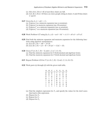
![7.30 Find a minimum four-level NAND- or NOR-gate circuit to realize
(a)
(b)
7.31 Implement using four NOR gates.
7.32 Implement using a three-level NAND-gate circuit.
7.33 Design a logic circuit that has a 4-bit binary number as an input and one output.The
output should be 1 iff the input is a prime number (greater than 1) or zero.
(a) Use a two-level NAND-gate circuit.
(b) Use a two-level NOR-gate circuit.
(c) Use only two-input NAND gates.
7.34 Work Problem 7.33 for a circuit that has an output 1 iff the input is evenly divisible
by 3 (0 is divisible by 3).
7.35 Realize the following functions, using only two-input NAND gates. Repeat using
only two-input NOR gates.
(a)
(b)
7.36 (a) Find a minimum circuit of two-input AND and two-input OR gates to realize
(b) Convert your circuit to two-input NAND gates.Add inverters where necessary.
(c) Repeat (b), except convert to two-input NOR gates.
7.37 Realize using NOR gates.Add inverters if necessary.
7.38 In which of the following two-level circuit forms can an arbitrary switching function
be realized? Verify your answers. (Assume the inputs are available in both comple-
mented and uncomplemented form.)
(a) NOR-AND
(b) NOR-OR
(c) NOR-NAND
(d) NOR-XOR
(e) NAND-AND
(f) NAND-OR
(g) NAND-NOR
(h) NAND-XOR
7.39 Find a minimum two-level, multiple-output AND-OR gate circuit to realize these
functions (eight gates minimum).
f3 (a, b, c, d) m(4, 11, 13, 14, 15) d(5, 9, 12)
f2 (a, b, c, d) m(0, 4, 8, 9) d(1, 10, 12)
f1 (a, b, c, d) m(10, 11, 12, 15) d(4, 8, 14)
Z A[BC D E(F GH)]
F(A, B, C, D) m(0, 1, 2, 3, 4, 5, 7, 9, 11, 13, 14, 15)
F A CD AB C D ABD BC
F A BC BD AC B CD
x yz xvy w xvy z
abde a b c
Z (a b e f )(c a b)(d a b)(g h)
Z abe f c e f d e f gh
Multi-Level Gate Circuits NAND and NOR Gates 213](https://image.slidesharecdn.com/fundamentalsoflogicdesign6thcharlesh-240226091353-b43ce575/85/Fundamentals-of-Logic-Design-6th-Charles-H-Roth-pdf-236-320.jpg)


![7. Study Section 8.5, Simulation and Testing of Logic Circuits.
(a) Verify that Table 8-1 is correct. Consider both the case where the unknown
value, X, is 0 and the case where it is 1.
(b) The following circuit was designed to realize the function
F [A B C D] [A B (C D )(C D)]
When a student builds the circuit in lab, he finds that when A C 0 and B
D 1, the output F has the wrong value and that the gate outputs are as shown.
Determine some possible causes of the incorrect output if G 0 and if G 1.
(c) Work Problems 8.4 and 8.5.
8. Study your assigned design problem and prepare a design which meets specifi-
cations. Note that only two-, three-, and four-input NAND gates (or NOR gates
as specified) and inverters are available for this project; therefore, factoring
some of the equations will be necessary. Try to make an economical design by
using common terms; however, do not waste time trying to get an absolute min-
imum solution. When counting gates, count both NAND (or NOR) gates and
inverters, but do not count the inverters needed for the input variables.
9. Check your design carefully before simulating it. Test it on paper by applying
some input combinations of 0’s and 1’s and tracing the signals through to make
sure that the outputs are correct. If you have a CAD program such as LogicAid
available, enter the truth table for your design into the computer, derive the
minimum two-level equations, and compare them with your solution.
10. In designing multi-level, multiple-output circuits of the type used in the design
problems in this unit, it is very difficult and time-consuming to find a minimum
solution. You are not expected to find the best possible solution to these prob-
lems. All of these solutions involve some “tricks,” and it is unlikely that you
could find them without trying a large number of different ways of factoring
your equations. Therefore, if you already have an acceptable solution, do not
waste time trying to find the minimum solution. Because integrated circuit gates
are quite inexpensive, it is not good engineering practice to spend a large
amount of time finding the absolute minimum solution unless a very large num-
ber of units of the same type are to be manufactured.
11. Obtain a Unit 8 supplement from your instructor and follow the instructions
therein regarding simulating and testing your design.
C′
D′
C
C A′
B
A
F
B′
D′
G
0
1 0
0
1
0
D
1
3 5
7
6
4
2
218 Unit 8](https://image.slidesharecdn.com/fundamentalsoflogicdesign6thcharlesh-240226091353-b43ce575/85/Fundamentals-of-Logic-Design-6th-Charles-H-Roth-pdf-241-320.jpg)


![Combinational Circuit Design and Simulation Using Gates 221
a
c
a′
b
d′
d′
b
a′
c
b′ f
a
c′
c'
FIGURE 8-1
FIGURE 8-2
f1 = Σ m(0, 2, 3, 4, 5) f2 = Σ m(0, 2, 3, 4, 7) f3 = Σ m(1, 2, 6, 7)
1 1
0 1
1
1
1
00
bc
a
01
11
10
1 1
0 1
1 1
1
00
bc
a
01
11
10
0 1
1
1
1
00
bc
a
01
11
10 1
As can be seen from the preceding expression, a two-level realization requires two
four-input gates and one five-input gate. The expression for f is factored to reduce
the maximum number of gate inputs to three and, then, it is complemented:
f b d(a c ac) a c(b d ) abc
f [b d (a c)(a c )][a c b d][a b c]
The resulting NOR-gate circuit is shown in Figure 8-1.
The techniques for designing two-level, multiple-output circuits given in
Section 7.6 are not very effective for designing multiple-output circuits with more
than two levels. Even if the two-level expressions had common terms, most of these
common terms would be lost when the expressions were factored.Therefore, when
designing multiple-output circuits with more than two levels, it is usually best to
minimize each function separately. The resulting two-level expressions must then
be factored to increase the number of levels. This factoring should be done in such
a way as to introduce common terms wherever possible.
Realize the functions given in Figure 8-2, using only two-input NAND gates and
Example inverters. If we minimize each function separately, the result is
f1 b c ab a b
f2 b c bc a b
f3 a b c ab bc](https://image.slidesharecdn.com/fundamentalsoflogicdesign6thcharlesh-240226091353-b43ce575/85/Fundamentals-of-Logic-Design-6th-Charles-H-Roth-pdf-244-320.jpg)


![this behavior is said to have an inertial delay. Quite often the inertial delay value is
assumed to be the same as the propagation delay of the gate; if this is the case, the
circuit of Figure 8-8 will generate the 0 glitch only for inverter delays greater than
10 ns. In contrast, if a gate always responds to input changes (with a propagation
delay), no matter how closely spaced the input changes may be, the gate is said to
have an ideal or transport delay. If the OR gate in Figure 8-8 has an ideal delay, then
the 0 glitch would be generated for any nonzero value of the inverter delay. (Inertial
and transport delay models are discussed more in Unit 10.) Unless otherwise noted,
the examples and problems in this unit assume that gates have an ideal delay.
Hazards can be detected using a Karnaugh map [Figure 8-8(a)]. As seen on the
map, no loop covers both minterms ABC and AB C. So if A C 1 and B changes,
both terms can momentarily go to 0, resulting in a glitch in F.We can detect hazards
in a two-level AND-OR circuit, using the following procedure:
1. Write down the sum-of-products expression for the circuit.
2. Plot each term on the map and loop it.
3. If any two adjacent 1’s are not covered by the same loop, a 1-hazard exists for
the transition between the two 1’s. For an n-variable map, this transition occurs
when one variable changes and the other n1 variables are held constant.
If we add a loop to the map of Figure 8-8(a) and, then, add the corresponding
gate to the circuit (Figure 8-9), this eliminates the hazard. The term AC remains 1
while B is changing, so no glitch can appear in the output. Note that F is no longer
a minimum sum of products.
Combinational Circuit Design and Simulation Using Gates 225
0 ns 10 ns 20 ns 30 ns
(b) Timing chart
(a) Circuit with a static 1-hazard
40 ns 50 ns
1-hazard
60 ns
F
E
D
B
B
A D
E
F
C F = AB′ + BC
0 1
0 1
1
0
1
0
1
0
00
BC
A
01
11
10
FIGURE 8-8
Detection of a
1-Hazard](https://image.slidesharecdn.com/fundamentalsoflogicdesign6thcharlesh-240226091353-b43ce575/85/Fundamentals-of-Logic-Design-6th-Charles-H-Roth-pdf-248-320.jpg)


![Multiplexers, Decoders, and Programmable Logic Devices 273
to 0 in Equation (9-8), and, then, setting xi to 1. Because both sides of the equation
are equal for xi 0 and for xi 1, the theorem is true for switching algebra.
Applying the expansion theorem to a 5-variable function gives
f(a, b, c, d, e) a f(0, b, c, d, e) a f(1, b, c, d, e) a f0 a f1 (9-9)
This shows that any 5-variable function can be realized using two 4-variable
function generators and a 2-to-1 MUX [Figure 9-36(a)]. This implies that any
5-variable function can be implemented using a CLB of the type shown in
Figure 9-33.
To realize a 6-variable function using 4-variable function generators, we apply
the expansion theorem twice:
G(a, b, c, d, e, f) a G(0, b, c, d, e, f) a G(1, b, c, d, e, f) a G0 a G1
G0 b G(0, 0, c, d, e, f) b G(0, 1, c, d, e, f) b G00 b G01
G1 b G(1, 0, c, d, e, f) b G(1, 1, c, d, e, f) b G10 bG11
Because G00,G01,G10,and G11 are all 4-variable functions,we can realize any 6-variable
function using four 4-variable function generators and three 2-to-1 MUXes, as shown
in Figure 9-36(b). Thus, we can realize any 6-variable function using two CLBs of the
type shown in Figure 9-31.Alternatively, we can write
G(a, b, c, d, e, f) a b G00 a b G01 ab G10 ab G11 (9-10)
and realize G using four function generators and a 4-to-1 MUX. In general, we can
realize any n-variable function (n 4) using 2n4
4-variable function generators
and one 2n4
-to-1 MUX. This is a worst-case situation because many functions of
n variables can be realized with fewer function generators.
b
b
c
d G00
G0
G1
G
G01
G10
G11
e
f
c
d
e
f
c
d
e
f
c
d
e
f
FG
FG
a
a
b
c F0
F1
F
d
e
FG
0
1
b
c
d
e
FG
(a) 5-variable function (b) 6-variable function
FG
FG
FIGURE 9-36
Realization of
5- and 6-Variable
Functions with
Function
Generators](https://image.slidesharecdn.com/fundamentalsoflogicdesign6thcharlesh-240226091353-b43ce575/85/Fundamentals-of-Logic-Design-6th-Charles-H-Roth-pdf-296-320.jpg)


![gate input changes, the gate output is recomputed by the hardware, and the output
changes after the gate delay.
When we initially describe a circuit, we may not be concerned about propaga-
tion delays. If we write
C A and B;
E C or D;
this implies that the propagation delays are 0 ns. In this case, the simulator will
assume an infinitesimal delay referred to as (delta). Assume that initially A 1
and B C D E 0. If B is changed to 1 at time 1 ns, then C will change at
time 1 and E will change at time 1 2.
Unlike a sequential program, the order of the above concurrent statements is
unimportant. If we write
E C or D;
C A and B;
the simulation results would be exactly the same as before.
In general, a signal assignment statement has the form
signal_name expression [after delay];
The expression is evaluated when the statement is executed, and the signal on the
left side is scheduled to change after delay. The square brackets indicate that after
delay is optional; they are not part of the statement. If after delay is omitted, then
the signal is scheduled to be updated after a delta delay. Note that the time at
which the statement executes and the time at which the signal is updated are not
the same.
Even if a VHDL program has no explicit loops, concurrent statements may exe-
cute repeatedly as if they were in a loop. Figure 10-2 shows an inverter with the
output connected back to the input. If the output is ‘0’, then this ‘0’ feeds back to
the input and the inverter output changes to ‘1’ after the inverter delay, assumed to
be 10 ns.Then, the ‘1’ feeds back to the input, and the output changes to ‘0’ after the
inverter delay.The signal CLK will continue to oscillate between ‘0’ and ‘1’, as shown
in the waveform. The corresponding concurrent VHDL statement will produce the
same result. If CLK is initialized to ‘0’, the statement executes and CLK changes to
‘1’ after 10 ns. Because CLK has changed, the statement executes again, and CLK
will change back to ‘0’ after another 10 ns. This process will continue indefinitely.
Introduction to VHDL 287
CLK
CLK
10 20 30 40 60
50
CLK = not CLK after 10 ns;
FIGURE 10-2
Inverter with
Feedback](https://image.slidesharecdn.com/fundamentalsoflogicdesign6thcharlesh-240226091353-b43ce575/85/Fundamentals-of-Logic-Design-6th-Charles-H-Roth-pdf-310-320.jpg)


![10.2 VHDL Models for Multiplexers
Figure 10-5 shows a 2-to-1 multiplexer (MUX) with two data inputs and one control
input.The MUX output is F A I0 A I1.The corresponding VHDL statement is
F (not A and I0) or (A and I1);
Alternatively, we can represent the MUX by a conditional signal assignment state-
ment, as shown in Figure 10-5. This statement executes whenever A, I0, or I1
changes. The MUX output is I0 when A ‘0’, and else it is I1. In the conditional
statement, I0, I1, and F can either be bits or bit-vectors.
290 Unit 10
D
C
B
0
1
E
F
A
0
1
F = A when E = '1'
else B when D = '1'
else C;
FIGURE 10-6
Cascaded 2-to-1
MUXes
A
F
I0
I1
0
1
-- conditional signal assignment statement
F = I0 when A = '0' else I1;
FIGURE 10-5
2-to-1 Multiplexer
The general form of a conditional signal assignment statement is
signal_name expression1 when condition1
else expression2 when condition2
[else expressionN];
This concurrent statement is executed whenever a change occurs in a signal used in
one of the expressions or conditions. If condition1 is true, signal_name is set equal
to the value of expression1, or else if condition2 is true, signal_name is set equal to
the value of expression2, etc. The line in square brackets is optional. Figure 10-6
shows how two cascaded MUXes can be represented by a conditional signal assign-
ment statement. The output MUX selects A when E ‘1’; or else it selects the out-
put of the first MUX, which is B when D ‘1’, or else it is C.
Figure 10-7 shows a 4-to-1 MUX with four data inputs and two control inputs,A
and B. The control inputs select which one of the data inputs is transmitted to the
output. The logic equation for the 4-to-1 MUX is
F A’B’I0 A’BI1 AB’I2 ABI3
Thus, one way to model the MUX is with the VHDL statement
F (not A and not B and I0) or (not A and B and I1) or
(A and not B and I2) or (A and B and I3);](https://image.slidesharecdn.com/fundamentalsoflogicdesign6thcharlesh-240226091353-b43ce575/85/Fundamentals-of-Logic-Design-6th-Charles-H-Roth-pdf-313-320.jpg)
![Introduction to VHDL 291
A B
I0
I1
I2
I3
F
MUX
sel = AB;
-- selected signal assignment statement
with sel select
F = I0 when 00,
I1 when 01,
I2 when 10,
I3 when 11;
FIGURE 10-7
4-to-1 Multiplexer
Another way to model the 4-to-1 MUX is to use a conditional assignment statement:
F I0 when AB “00”
else I1 when AB “01”
else I2 when AB “10”
else I3;
The expression AB means A concatenated with B, that is, the two bits A and B
are merged together to form a 2-bit vector.This bit vector is tested, and the appro-
priate MUX input is selected. For example, if A ‘1’ and B ‘0’, AB “10”
and I2 is selected. Instead of concatenating A and B, we could use a more complex
condition:
F I0 when A ‘0’ and B ‘0’
else I1 when A ‘0’ and B ‘1’
else I2 when A ‘1’ and B ‘0’
else I3;
A third way to model the MUX is to use a selected signal assignment state-
ment, as shown in Figure 10-7. AB cannot be used in this type of statement, so
we first set Sel equal to AB. The value of Sel then selects the MUX input that is
assigned to F.
The general form of a selected signal assignment statement is
with expression_s select
signal_s expression1 [after delay-time] when choice1,
expression2 [after delay-time] when choice2,
. . .
[expression_n [after delay-time] when others];
This concurrent statement executes whenever a signal changes in any of the
expressions. First, expression_s is evaluated. If it equals choice1, signal_s is set
equal to expression1; if it equals choice2, signal_s is set equal to expression2; etc. If
all possible choices for the value of expression_s are given, the last line should be
omitted; otherwise, the last line is required.When it is present, if expression_s is not
equal to any of the enumerated choices, signal_s is set equal to expression_n. The
signal_s is updated after the specified delay-time, or after if the “after delay-
time” is omitted.](https://image.slidesharecdn.com/fundamentalsoflogicdesign6thcharlesh-240226091353-b43ce575/85/Fundamentals-of-Logic-Design-6th-Charles-H-Roth-pdf-314-320.jpg)
![10.3 VHDL Modules
To write a complete VHDL module, we must declare all of the input and output
signals using an entity declaration, and then specify the internal operation of the
module using an architecture declaration. As an example, consider Figure 10-8. The
entity declaration gives the name “two_gates” to the module. The port declaration
specifies the inputs and outputs to the module.A, B, and D are input signals of type
bit, and E is an output signal of type bit. The architecture is named “gates”. The
signal C is declared within the architecture because it is an internal signal. The two
concurrent statements that describe the gates are placed between the keywords
begin and end.
292 Unit 10
...
Entity
Architecture
Module 1
Entity
Architecture
Module 2
Entity
Architecture
Entity
Architecture
Module N
FIGURE 10-9
VHDL Program
Structure
entity two_gates is
port (A,B,D: in bit; E: out bit);
end two_gates;
architecture gates of two_gates is
signal C: bit;
begin
C = A and B; -- concurrent
E = C or D; -- statements
end gates;
A
B
D
C
E
FIGURE 10-8
VHDL Module with
Two Gates
When we describe a system in VHDL, we must specify an entity and an
architecture at the top level, and also specify an entity and architecture for each of
the component modules that are part of the system (see Figure 10-9). Each entity
declaration includes a list of interface signals that can be used to connect to other
modules or to the outside world. We will use entity declarations of the form:
entity entity-name is
[port(interface-signal-declaration);]
end [entity] [entity-name];
The items enclosed in square brackets are optional.The interface-signal-declaration
normally has the following form:
list-of-interface-signals: mode type [: initial-value]
{; list-of-interface-signals: mode type [: initial-value]};](https://image.slidesharecdn.com/fundamentalsoflogicdesign6thcharlesh-240226091353-b43ce575/85/Fundamentals-of-Logic-Design-6th-Charles-H-Roth-pdf-315-320.jpg)
![The curly brackets indicate zero or more repetitions of the enclosed clause. Input
signals are of mode in, output signals are of mode out, and bi-directional signals (see
Figure 9-12) are of mode inout.
So far, we have only used type bit and bit_vector; other types are described in
Section 10.4. The optional initial-value is used to initialize the signals on the associ-
ated list; otherwise, the default initial value is used for the specified type. For exam-
ple, the port declaration
port(A, B: in integer : 2; C, D: out bit);
indicates that A and B are input signals of type integer that are initially set to 2, and
C and D are output signals of type bit that are initialized by default to ‘0’.
Associated with each entity is one or more architecture declarations of the
form
architecture architecture-name of entity-name is
[declarations]
begin
architecture body
end [architecture] [architecture-name];
In the declarations section, we can declare signals and components that are used
within the architecture.The architecture body contains statements that describe the
operation of the module.
Next, we will write the entity and architecture for a full adder module (refer
to Section 4.7 for a description of a full adder).The entity specifies the inputs and
outputs of the adder module, as shown in Figure 10-10.The port declaration spec-
ifies that X, Y and Cin are input signals of type bit, and that Cout and Sum are
output signals of type bit.
Introduction to VHDL 293
X
Y
Cin
Cout
Sum
Full
Adder
entity FullAdder is
port (X,Y,Cin: in bit; -- Inputs
Cout, Sum: out bit); -- Outputs
end FullAdder;
FIGURE 10-10
Entity Declaration
for a Full Adder
Module
The operation of the full adder is specified by an architecture declaration:
In this example, the architecture name (Equations) is arbitrary, but the entity name
(FullAdder) must match the name used in the associated entity declaration.
architecture Equations of FullAdder is
begin -- concurrent assignment statements
Sum X xor Y xor Cin after 10 ns;
Cout (X and Y) or (X and Cin) or (Y and Cin) after 10 ns;
end Equations;](https://image.slidesharecdn.com/fundamentalsoflogicdesign6thcharlesh-240226091353-b43ce575/85/Fundamentals-of-Logic-Design-6th-Charles-H-Roth-pdf-316-320.jpg)


![The port clause used in the component declaration has the same form as the port
clause used in an entity declaration. The connections to each component used in a
circuit are specified by using a component instantiation statement of the form
label: component-name port map (list-of-actual-signals);
The list of actual signals must correspond one-to-one to the list of interface signals
specified in the component declaration.
10.4 Signals and Constants
Input and output signals for a module are declared in a port. Signals internal to a
module are declared at the start of an architecture, before begin, and can be used
only within that architecture. Port signals have an associated mode (usually in or
out), but internal signals do not. A signal used within an architecture must be
declared either in a port or in the declaration section of an architecture, but it can-
not be declared in both places. A signal declaration has the form
signal list_of_signal_names: type_name [constraint] [: initial_value];
The constraint can be an index range like (0 to 5) or (4 downto 1), or it can be a
range of values such as range 0 to 7. Examples:
signal A, B, C: bit_vector(3 downto 0): “1111”;
A, B, and C are 4-bit vectors dimensioned 3 downto 0 and initialized to 1111.
signal E, F: integer range 0 to 15;
E and F are integers in the range 0 to 15, initialized by default to 0. The compiler or
simulator will flag an error if we attempt to assign a value outside the specified range
to E or F.
Constants declared at the start of an architecture can be used anywhere within
that architecture. A constant declaration is similar to a signal declaration:
constant constant_name: type_name [constraint] [: constant_value];
A constant named limit of type integer with a value of 17 can be defined as
constant limit : integer : 17;
A constant named delay1 of type time with the value of 5 ns can be defined as
constant delay1 : time : 5 ns;
This constant could then be used in an assignment statement
A B after delay1;
Once the value of a constant is defined in a declaration statement, unlike a signal,
the value cannot be changed by using an assignment statement.
Signals and constants can have any one of the predefined VHDL types, or they
can have a user-defined type. Some of the predefined types are
Introduction to VHDL 297](https://image.slidesharecdn.com/fundamentalsoflogicdesign6thcharlesh-240226091353-b43ce575/85/Fundamentals-of-Logic-Design-6th-Charles-H-Roth-pdf-320-320.jpg)

![DATA_WORD is a signal array of 16 bits, indexed 15 downto 0, which is ini-
tialized (by default) to all ‘0’ bits. ALT_WORD is a signal array of 16 bits which is
initialized to alternating 0’s and 1’s. ONE_WORD is a constant array of 16 bits; all
bits are set to ‘1’ by (others ‘1’). Because none of the bits have been set indi-
vidually,1
in this case others applies to all of the bits.
We can reference individual elements of the array by specifying an index value.
For example,ALT_WORD(0) accesses the far right bit of ALT_WORD.We can also
specify a portion of the array by specifying an index range:ALT_WORD(5 downto 0)
accesses the low order six bits of ALT_WORD, which have an initial value of 010101.
The array type and array object declarations illustrated above have the general
forms:
type array_type_name is array index_range of element_type;
signal array_name: array_type_name [ : initial_values ];
In this declaration, signal may be replaced with constant.
Multidimensional array types may also be defined with two or more dimensions.
The following example defines a two-dimensional array signal which is a matrix of
integers with four rows and three columns:
type matrix4x3 is array (1 to 4, 1 to 3) of integer;
signal matrixA: matrix4x3 : ((1,2,3),(4,5,6),(7,8,9),(10,11,12));
The signal matrixA, will be initialized to
The array element matrixA(3,2) references the element in the third row and second col-
umn, which has a value of 8.The statement B matrixA(2,3) assigns a value of 6 to B.
When an array type is declared, the dimensions of the array may be left unde-
fined. This is referred to as an unconstrained array type. For example,
type intvec is array (natural range ) of integer;
declares intvec as an array type which defines a one-dimensional array of integers with
an unconstrained index range of natural numbers.The default type for array indices is
integer, but another type may be specified. Because the index range is not specified in
the unconstrained array type, the range must be specified when the array object is
declared. For example,
signal intvec5: intvec(1 to 5) : (3,2,6,8,1);
defines a signal array named intvec5 with an index range of 1 to 5, which is initial-
ized to 3, 2, 6, 8, 1. The following declaration defines matrix as a two-dimensional
array with unconstrained row and column index ranges:
type matrix is array (natural range , natural range ) of integer;
1 2 3
4 5 6
7 8 9
10 11 12
Introduction to VHDL 299
1
See Reference [1, p. 86] for information on how to set individual bits.](https://image.slidesharecdn.com/fundamentalsoflogicdesign6thcharlesh-240226091353-b43ce575/85/Fundamentals-of-Logic-Design-6th-Charles-H-Roth-pdf-322-320.jpg)


![The shift operators are used to shift or rotate a bit_vector. In the following
examples, A is an 8- bit vector equal to “10010101”:
A sll 2 is “01010100” (shift left logical, filled with ‘0’)
A srl 3 is “00010010” (shift right logical, filled with ‘0’)
A sla 3 is “10101111” (shift left arithmetic, filled with rightmost bit)
A sra 2 is “11100101” (shift right arithmetic, filled with leftmost bit)
A rol 3 is “10101100” (rotate left)
A ror 5 is “10101100” (rotate right)
We will not utilize these shift operators because some software used for synthesis
uses different shift operators. Instead, we will do shifting using the concatenation
operator. For example, if A in the above listing is dimensioned 7 downto 0, we can
implement shift right arithmetic two places as follows:
A(7)A(7)A(7 downto 2) ‘1’’1’“100101” “11100101”
This makes two copies of the sign bit followed by the left 6 bits of A, which gives the
same result as A sra 2.
The and operators can be applied to integer or real numeric operands. The
operator can be used to concatenate two vectors (or an element and a vector, or
two elements) to form a longer vector. For example, “010” ‘1’ is “0101” and
“ABC” “DEF” is “ABCDEF.”
The * and / operators perform multiplication and division on integer or float-
ing-point operands.The rem and mod operators calculate the remainder and mod-
ulus for integer operands. (We will not use rem and mod; for further discussion of
these operators see Reference [1].) The ** operator raises an integer or floating-
point number to an integer power, and abs finds the absolute value of a numeric
operand.
10.7 Packages and Libraries
Packages and libraries provide a convenient way of referencing frequently used
functions and components. A package consists of a package declaration and an
optional package body. The package declaration contains a set of declarations
which may be shared by several design units. For example, it may contain type, sig-
nal, component, function, and procedure declarations. The package body usually
contains component descriptions and the function and procedure bodies.The pack-
age and its associated compiled VHDL models may be placed in a library, so they
can be accessed as required by different VHDL designs.A package declaration has
the form:
package package-name is
package declarations
end [package][package-name];
302 Unit 10](https://image.slidesharecdn.com/fundamentalsoflogicdesign6thcharlesh-240226091353-b43ce575/85/Fundamentals-of-Logic-Design-6th-Charles-H-Roth-pdf-325-320.jpg)
![A package body has the form
package body package-name is
package body declarations
end [package body][package name];
We have developed a package called bit_pack which is used in a number of exam-
ples in this book. This package contains commonly used components and functions
which use signals of type bit and bit_vector. A complete listing of this package and
associated component models is included on the CD-ROM that accompanies this
text. Most of the components in this package have a default delay of 10 ns, but this
delay can be changed by the use of generics. For an explanation of generics, refer to
one of the VHDL references. We have compiled this package and the component
models and placed the result in a library called BITLIB.
One of the components in the library is a two-input NOR gate named Nor2,
which has default delay of 10 ns. The package declaration for bit_pack includes the
component declaration
component Nor2
port (A1, A2: in bit; Z: out bit);
end component;
The NOR gate is modeled using a concurrent statement. The entity-architecture
pair for this component is
-- two-input NOR gate
entity Nor2 is
port (A1, A2: in bit; Z: out bit);
end Nor2;
architecture concur of Nor2 is
begin
Z not(A1 or A2) after 10 ns;
end concur;
To access components and functions within a package requires a library state-
ment and a use statement. The statement
library BITLIB;
allows your design to access the BITLIB. The statement
use BITLIB.bit_pack.all;
allows your design to use the entire bit_pack package. A statement of the form
use BITLIB.bit_pack.Nor2;
may be used if you want to use a specific component (in this case Nor2) or function
in the package.
When components from a library package are used, component declarations are
not needed. Figure 10-15 shows a NOR-NOR circuit and the corresponding struc-
tural VHDL code. This code instantiates three copies of the Nor2 gate component
from the package bit_pack and connects the gate inputs and outputs.
Introduction to VHDL 303](https://image.slidesharecdn.com/fundamentalsoflogicdesign6thcharlesh-240226091353-b43ce575/85/Fundamentals-of-Logic-Design-6th-Charles-H-Roth-pdf-326-320.jpg)


![Introduction to VHDL 313
For the six input combinations that do not represent valid BCD digits, the circuit
output should be “XXXX”. Make the inputs and outputs of type std_logic.
(a) Write the code using the when else assignment statement.
(b) Use the VHDL simulator to verify the code of Part (a) for the inputs x 0100,
0101, 1001, and 1010.
(c) Write the code using the with select when assignment statement.
(d) Use the VHDL simulator to verify the code of Part (c) for the inputs x 0100,
0101, 1001, and 1010.
10.22 Write VHDL code that gives a behavioral description of a circuit that converts the
representation of decimal digits in the weighted code with weights 8, 4, 2 and 1
to the representation using the excess-3 code.
(a) Write the code using the when else assignment statement.
(b) Use the VHDL simulator to verify the code of Part (a) for the inputs x 0011,
0100, 1001, and 1010.
(c) Write the code using the with select when assignment statement.
(d) Use the VHDL simulator to verify the code of Part (c) for the inputs x 0100,
0101, 1001, and 1010.
Design Problems
10.A (a) Design a 4-to-1 MUX using only three 2-to-1 MUXes. Write an entity-architec-
ture pair to implement a 2-to-1 MUX. Then write an entity-architecture pair to
implement a 4-to-1 MUX using three instances of your 2-to-1 MUX.
[Hint: The equation for a 4-to-1 MUX can be rewritten as
F A (I0B I1B) A (I2B I3B)].
Use the following port definitions:
For the 2-to-1 MUX:
port (i0, i1: in bit; sel: in bit; z: out bit);
For the 4-to-1 MUX:
port (i0, i1, i2, i3: in bit; a, b: in bit; f: out bit);
(b) Simulate your code and test it using the following inputs:
I0 I2 1, I1 I3 0, AB 00, 01, 11, 10
10.B (a) Show how a BCD to Gray code converter can be designed using a 16 words
4 bits ROM. Then write an entity-architecture pair to implement the converter
using the ROM. For your code to function correctly, you will need to add the
following two lines of code to the top of your program.
library BITLIB;
use BITLIB.bit_pack.all;
Use the port definition specified below for the ROM:
port (bcd: in bit_vector (3 downto 0);
gray: out bit_vector (3 downto 0));](https://image.slidesharecdn.com/fundamentalsoflogicdesign6thcharlesh-240226091353-b43ce575/85/Fundamentals-of-Logic-Design-6th-Charles-H-Roth-pdf-336-320.jpg)

![(b) Simulate your code and test it using the following inputs:
a b c 0 0 0, 1 0 0, 1 0 1, 0 0 1, 0 1 1
10.G (a) Write the VHDL code for a full subtracter, using logic equations. Assume that
the full subtracter has a 5-ns delay.
(b) Write the VHDL code for a 4-bit subtracter using the module defined in (a) as a
component.
(c) Simulate your code and test it using the following inputs:
1100 – 0101, 0110 – 1011
10.H (a) The diagram shows an 8-bit shifter that shifts its input one place to the left.
Write a VHDL module for the shifter.
(b) Write a VHDL module that multiplies an 8-bit input (C) by 1012 to give a 11-bit
product (D). This can be accomplished by shifting C two places to the left and
adding the result to C. Use two of the modules written in (a) as components and
an overloaded operator for addition.
(c) Simulate your code and test it using the following inputs:
10100101 11111111
10.I (a) Design a 4-to-2 priority encoder using gates [see Unit 9, Study Guide, Part 4(b)].
Write a VHDL module for your encoder. Use the port declaration
Port ( y : in std_logic_vector(0 to 3);
a1,b1,c1: out std_logic);
(b) Design an 8-to-3 priority encoder (Figure 9-16), using two instances of the 4-to-2
priority encoder you designed, two 2-to-1 multiplexers, and one OR gate.Write a
VHDL module for the 8-to-3 encoder. Use the port declaration
Port ( y : in std_logic_vector(0 to 7);
a,b,c,d : out std_logic);
(Hint: In building the 8-to-3 encoder, use one 4-to-2 encoder for the four most
significant bits, and the other for the four least significant bits. Outputs b and c
of the 8-to-3 encoder should come from the multiplexers.)
(c) Simulate your code and test it using the following inputs:
00000000, 10000000, 11000000, ---, 11111111
10.J (a) Write a VHDL module for a 4-bit adder, with a carry-in and carry-out, using an
overloaded addition operator and std_logic_vector inputs and outputs.
B (7 down to 0)
A (7 down to 0)
Lout Rin
Introduction to VHDL 315](https://image.slidesharecdn.com/fundamentalsoflogicdesign6thcharlesh-240226091353-b43ce575/85/Fundamentals-of-Logic-Design-6th-Charles-H-Roth-pdf-338-320.jpg)


![324 Unit 11
If S is changed back to 0, the circuit will not change state because Q 1 feeds
back into the first gate, causing P to remain 0, as shown in Figure 11-4(a). Note that
the inputs are again S R 0, but the outputs are different than those with which
we started. Thus, the circuit has two different stable states for a given set of inputs.
If we now change R to 1, Q will become 0 and P will then change back to 1, as seen
in Figure 11-4(b). If we then change R back to 0, the circuit remains in this state and
we are back where we started.
This circuit is said to have memory because its output depends not only on the
present inputs, but also on the past sequence of inputs. If we restrict the inputs so that
R S 1 is not allowed, the stable states of the outputs P and Q are always comple-
ments, that is, P Q . To emphasize the symmetry between the operation of the two
gates, the circuit is often drawn in cross-coupled form [see Figure 11-5(a)]. As shown
in Figures 11-3(b) and 11-4(b), an input S 1 sets the output to Q 1, and an input
R 1 resets the output to Q 0. When used with the restriction that R and S cannot
be 1 simultaneously, the circuit is commonly referred to as a set-reset (S-R) latch and
given the symbol shown in Figure 11-5(b).Note that although Q comes out of the NOR
gate with the R input, the standard S-R latch symbol has Q directly above the S input.
If S R 1, the latch will not operate properly, as shown in Figure 11-6. The
notation 1 S 0 means that the input is originally 1 and then changes to 0. Note that
when S and R are both l, P and Q are both 0. Therefore, P is not equal to Q , and
this violates a basic rule of latch operation that requires the latch outputs to be com-
plements. Furthermore, if S and R are simultaneously changed back to 0, P and Q
may both change to 1. If S R 0 and P Q l, then after the 1’s propagate
S
P
0
(a)
Q
1
0
R 0
S
P
1
(b)
Q
0
0
R 1
FIGURE 11-4
Q
R
Q′
R
Q
S
S
Q′
L
(a) (b)
FIGURE 11-5
S-R Latch
S
R
P 0→1→0→1
Q 0→1→0→1
1→0
1→0
FIGURE 11-6
Improper S-R Latch
Operation](https://image.slidesharecdn.com/fundamentalsoflogicdesign6thcharlesh-240226091353-b43ce575/85/Fundamentals-of-Logic-Design-6th-Charles-H-Roth-pdf-347-320.jpg)
![Latches and Flip-Flops 325
through the gates, P and Q will become 0 again, and the latch may continue to
oscillate if the gate delays are equal.
Figure 11-7 shows a timing diagram for the S-R latch. Note that when S changes
to 1 at time tl, Q changes to 1 a short time () later. ( represents the response time
or delay time of the latch.) At time t2, when S changes back to 0, Q does not change.
At time t3, R changes to 1, and Q changes back to 0 a short time () later. The dura-
tion of the S (or R) input pulse must normally be at least as great as in order for a
change in the state of Q to occur. If S 1 for a time less than , the gate output will
not change and the latch will not change state.
When discussing latches and flip-flops, we use the term present state to denote the
state of the Q output of the latch or flip-flop at the time any input signal changes, and
the term next state to denote the state of the Q output after the latch or flip-flop has
reacted to the input change and stabilized. If we let Q(t) represent the present state
and Q(t ) represent the next state, an equation for Q(t ) can be obtained from
the circuit by conceptually breaking the feedback loop at Q and considering Q(t) as
an input and Q(t ) as the output. Then for the S-R latch of Figure 11-3
Q(t ) R(t) [S(t) Q(t)] R(t) S(t) R(t) Q(t) (11-1)
and the equation for output P is
P(t) S(t) Q(t) (11-2)
Normally we write the next-state equation without including time explicitly, using Q
to represent the present state of the latch and Q
to represent the next state:
Q
R S R Q (11-3)
P S Q (11-4)
These equations are mapped in the next-state and output tables of Table 11-1. The
stable states of the latch are circled.Note that for all stable states,P Q except when
S R 1. As discussed previously, this is one of the reasons why S R 1 is
R
S
Q
t1
t1 +
t2 t3 t4 t
t3 +
0 0
1
FIGURE 11-7
Timing Diagram
for S-R Latch
TABLE 11-1
S-R Latch
Next State
and Output
Present Next State Q
Present Output P
State SR SR SR SR SR SR SR SR
Q 00 01 11 10 00 01 11 10
0 0 0 0 1 1 1 0 0
1 1 0 0 1 0 0 0 0](https://image.slidesharecdn.com/fundamentalsoflogicdesign6thcharlesh-240226091353-b43ce575/85/Fundamentals-of-Logic-Design-6th-Charles-H-Roth-pdf-348-320.jpg)
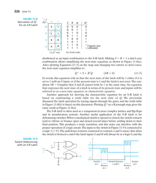

![328 Unit 11
11.4 Edge-Triggered D Flip-Flop
A D flip-flop (Figure 11-13) has two inputs, D (data) and Ck (clock). The small
arrowhead on the flip-flop symbol identifies the clock input. Unlike the D latch, the
flip-flop output changes only in response to the clock, not to a change in D.If the out-
put can change in response to a 0 to 1 transition on the clock input, we say that the
flip-flop is triggered on the rising edge (or positive edge) of the clock. If the output
can change in response to a 1 to 0 transition on the clock input, we say that the flip-
flop is triggered on the falling edge (or negative edge) of the clock.An inversion bub-
ble on the clock input indicates a falling-edge trigger (Figure 11-13(b)), and no bub-
ble indicates a rising-edge trigger [Figure 11-13(a)].The term active edge refers to the
clock edge (rising or falling) that triggers the flip-flop state change.
Q′ Q
Ck D
FF
(a) Rising-edge trigger
Q′ Q
D
FF
(b) Falling-edge trigger
Ck
D Q Q
0 0 0
0 1 0
1 0 1
1 1 1
FIGURE 11-13
D Flip-Flops
(c) Truth table
Q+
D
Q
Ck
1 0
1 0 1 1 0
1 1 0 0
D
FIGURE 11-14
Timing for
D Flip-Flop
(Falling-Edge
Trigger)
The state of a D flip-flop after the active clock edge (Q
) is equal to the input
(D) before the active edge. For example, if D 1 before the clock pulse, Q 1 after
the active edge, regardless of the previous value of Q. Therefore, the characteristic
equation is Q
D. If D changes at most once following each clock pulse, the out-
put of the flip-flop is the same as the D input, except that the output changes are
delayed until after the active edge of the clock pulse, as illustrated in Figure 11-14.
D
L
G
Q
Q′
Q+
= G′Q + GD
0 0 1 0
00 01 11 10
1 1 1 0
0
Q
GD
1
G D Q Q
0 0 0 0
0 0 1 1
0 1 0 0
0 1 1 1
1 0 0 0
1 0 1 0
1 1 0 1
1 1 1 1
FIGURE 11-12
Symbol and Truth
Table for Gated
Latch](https://image.slidesharecdn.com/fundamentalsoflogicdesign6thcharlesh-240226091353-b43ce575/85/Fundamentals-of-Logic-Design-6th-Charles-H-Roth-pdf-351-320.jpg)


![334 Unit 11
Q′
T
Q
Ck
Clock
J
(a) Conversion of J-K to T
K
Q′
Clock
Q
D
T
(b) Conversion of D to T
Ck
FIGURE 11-24
Implementation
of T Flip-Flops
Q′ Q
Ck
ClrN PreN
D
(a)
FIGURE 11-25
D Flip-Flop with
Clear and Preset
Ck D PreN ClrN Q
x x 0 0 (not allowed)
x x 0 1 1
x x 1 0 0
c 0 1 1 0
c 1 1 1 1
0,1,T x 1 1 Q (no change)
(b)
Q
t2
t1 t3 t4
T
tp tp
Ck
FIGURE 11-23
Timing Diagram
for T Flip-Flop
(Falling-Edge
Trigger)
One way to implement a T flip-flop is to connect the J and K inputs of a J-K flip-
flop together, as shown in Figure 11-24(a). Substituting T for J and K in the J-K
characteristic equation gives
Q
JQ K Q TQ T Q
which is the characteristic equation for the T flip-flop. Another way to realize a T
flip-flop is with a D flip-flop and an exclusive-OR gate [Figure 11-24(b)]. The D
input is Q ⊕ T, so Q
Q ⊕ T TQ T Q, which is the characteristic equation
for the T flip-flop.
11.8 Flip-Flops with Additional Inputs
Flip-flops often have additional inputs which can be used to set the flip-flops to an
initial state independent of the clock. Figure 11-25 shows a D flip-flop with clear and
preset inputs. The small circles (inversion symbols) on these inputs indicate that a
logic 0 (rather than a 1) is required to clear or set the flip-flop. This type of input is
often referred to as active-low because a low voltage or logic 0 will activate the clear](https://image.slidesharecdn.com/fundamentalsoflogicdesign6thcharlesh-240226091353-b43ce575/85/Fundamentals-of-Logic-Design-6th-Charles-H-Roth-pdf-357-320.jpg)


![change states in a prescribed sequence when input pulses are received. In this unit,
you will learn procedures for deriving flip-flop input equations for counters. These
procedures will be applied to more general types of sequential circuits in later units.
12.1 Registers and Register Transfers
Several D flip-flops may be grouped together with a common clock to form a register
[Figure 12-1(a)]. Because each flip-flop can store one bit of information, this register can
store four bits of information.This register has a load signal that isANDed with the clock.
354 Unit 12
Q3
D3
Clr
(a) Using gated clock
Data in
Data out
0→1
1
ClrN
Load
Clk
1 0 1
Q2
D2
Clr
0→1
Q1
D1
Clr
0→0
Q0
D0
Clr
0→1
Q3
D3
Clr
(b) With clock enable
(c) Symbol
Data in
Data out
0→1
1
Load
ClrN
Clk
1 0 1
Q2
D2
Clr
0→1
Q1
D1
Clr
0→0
Q0
D0
CE CE CE CE
Clr
Q
D
CE
Load Clk
4
4
Clr
ClrN
0→1
FIGURE 12-1
4-Bit D Flip-Flop
Registers with
Data, Load,
Clear, and
Clock Inputs](https://image.slidesharecdn.com/fundamentalsoflogicdesign6thcharlesh-240226091353-b43ce575/85/Fundamentals-of-Logic-Design-6th-Charles-H-Roth-pdf-377-320.jpg)


![By inspection of the table in Figure 12-17, we can verify that these are the correct
equations for a down counter. For every row of the table, A
A , so A changes
state every clock cycle. For those rows where A 0, B
B . For those rows where
B 0 and A 0, C
C .
Next, we will design a loadable counter [Figure 12-19(a)]. This counter has two
control signals Ld (load) and Ct (count). When Ld 1 binary data is loaded into
the counter on the rising clock edge, and when Ct 1, the counter is incremented
on the rising clock edge. When Ld Ct 0, the counter holds its present state.
When Ld Ct 1, load overrides count, and data is loaded into the counter. The
counter also has an asynchronous clear input that clears the counter when ClrN is
0. Figure 12-19(b) summarizes the counter operation.All state changes occur on the
rising edge of the clock (except for the asynchronous clear).
Figure 12-20 shows how the loadable counter can be implemented using flip-
flops, MUXes, and gates. When Ld 1, each MUX selects a Di input, and because
the output of each AND gate is 0, the output of each XOR gate is Di, which gets
stored in a flip-flop.When Ld 0 and Ct 1, each MUX selects one of the flip-flop
outputs (C, B, or A). The circuit then becomes equivalent to Figure 12-15, and the
counter is incremented on the rising clock edge.
The next-state equations for the counter of Figure 12-20 are
A
DA (Ld A Ld DAin) ⊕ Ld Ct
B
DB (Ld B Ld DBin) ⊕ Ld Ct A
C
DC (Ld C Ld DCin) ⊕ Ld Ct B A
366 Unit 12
(a)
Q
D
Clk
3
3
ClrN
Ct
Ld
ClrN Ld Ct C
B
A
0 X X 0 0 0
1 1 X DC DB DA (load)
1 0 0 C B A (no change)
1 0 1 Present state 1
(b)
FIGURE 12-19
Loadable Counter
with Count Enable
C
C′
Clk
Ld
Ld
Ct
DC
DCin
ClrN
B
B′
Clk
Ld
DB
DBin
ClrN
A
A′
Clk
Ld
DA
DAin
ClrN
FIGURE 12-20
Circuit for
Figure 12-19](https://image.slidesharecdn.com/fundamentalsoflogicdesign6thcharlesh-240226091353-b43ce575/85/Fundamentals-of-Logic-Design-6th-Charles-H-Roth-pdf-389-320.jpg)


![12.36 A digital system can perform any 4-variable bitwise logic function, but it may take
several clock cycles. (A bitwise logic function performs the same logic function on
each bit.) Recall that the NAND operation is functionally complete, i.e., we can do
any logic function by a series of NAND operations. On the following 8-bit registers,
En is a tri-state buffer enable as in Figure 12-3, and CE is a clock enable as in
Figure 12-1.
(a) Show how to connect a 2-to-4 decoder (with inverting outputs) so that the next
rising edge of the clock will load the result into register A, B, C, or D for con-
trol inputs G0G1 00, 01, 10, or 11, respectively.
(b) Show how to connect three control signals, E0, E1, and E2, to the registers so that
E0 0 places the A register contents on the X bus,E0 1 places B onto the X bus,
E1E2 00 places C onto the Y bus, E1E2 01 places D onto the Y bus, E1E2 10
places 00000000 on the Y bus, and E1E2 11 places 11111111 on the Y bus. You
may use a few additional gates. (Hint: Connect E2 to all 8 data inputs on the tri-
state buffer on the right side of the circuit.)
(c) Show how to make the bits in the C register be the OR of the corresponding bits in
the A register and in the D register,in four clock cycles.Tell what G0,G1,E0,E1,and
E2 should be for each cycle. [Hint: Use DeMorgan’s law and X (X NAND 1).]
12.37 Show how to make the shift register of Figure 12-10 reverse the order of its bits,
i.e., Q3
Q0, Q2
Q1, Q1
Q2, and Q0
Q3.
(a) Use external connections between the Q outputs and the D inputs.What should
the values of Sh and L be for a reversal?
CE
En A
CK
8 8
8 8
8
8 8
CE
En B
CK
CE
8 NAND Gates
En
R
X Y
C
CK
CE
En D
CK
8
8
386 Unit 12
Clock Input Accumulator Addend
Cycle Data EnIn EnAd LdAc LdAd Register Register Bus
0 18 1 0 1 0 0 0 18
1 13 1 0 0 1
2 15 0 1 1 0
3 93 1 0 0 1
4 47 0 1 1 0
5 22 1 0 0 1
6 0 0 1 0 0](https://image.slidesharecdn.com/fundamentalsoflogicdesign6thcharlesh-240226091353-b43ce575/85/Fundamentals-of-Logic-Design-6th-Charles-H-Roth-pdf-409-320.jpg)


![labels on the arrows between states are of the form X/Z, where the symbol before
the slash is the input and the symbol after the slash is the corresponding output.
Thus, in state S0 an input of 0 gives an output of 0, and an input of 1 gives an output
of 1. For any given input sequence, we can easily trace out the state and output
sequences on the state graph. For the input sequence X 10101, verify that the cor-
responding output sequence is 11001. This agrees with Figure 13-8 if the false out-
puts are ignored. Note that the false outputs do not show on the state graph because
the inputs are read at the active clock edge, and no provision is made for extra input
changes between active edges.
Next, we will analyze the operation of a serial adder [Figure 13-12(a)] that
adds two n-bit binary numbers X xn1 . . . x1x0 and Y yn1 . . . y1y0. The oper-
ation of the serial adder is similar to the parallel adder of Figure 4-2 except that
the binary numbers are fed in serially, one pair of bits at a time, and the sum is
read out serially, one bit at a time. First, x0 and y0 are fed in; a sum digit s0 is gen-
erated, and the carry c1 is stored. At the next clock time, x1 and y1 are fed in and
added to c1 to give the next sum digit s1 and the new carry c2, which is stored.
This process continues until all bits have been added. A full adder is used to add
the xi, yi, and ci bits to form ci1 and si. A D flip-flop is used to store the carry
(ci1) on the rising edge of the clock. The xi and yi inputs must be synchronized
with the clock.
Figure 13-13 shows a timing diagram for the serial adder. In this example we add
10011 00110 to give a sum of 11001 and a final carry of 0. Initially the carry flip-flop
must be cleared so that c0 0.We start by adding the least-significant (rightmost) bits
in each word.Adding 1 0 0 gives s0 1 and c1 0, which is stored in the flip-flop
404 Unit 13
Clock
CK
Q′
Q D
xi
yi
ci
si
ci + 1
(a) With D flip-flop
Full
Adder
FIGURE 13-12
Serial Adder
xi yi ci ci 1 si
0 0 0 0 0
0 0 1 0 1
0 1 0 0 1
0 1 1 1 0
1 0 0 0 1
1 0 1 1 0
1 1 0 1 0
1 1 1 1 1
(b) Truth table
S0
S3
S1
S2
0
0
1
0
1
1
1
1
0
0
1
1 0
0
0
1
FIGURE 13-11
Mealy State
Graph for
Figure 13-7](https://image.slidesharecdn.com/fundamentalsoflogicdesign6thcharlesh-240226091353-b43ce575/85/Fundamentals-of-Logic-Design-6th-Charles-H-Roth-pdf-427-320.jpg)


![so the receiver can read the data at the proper time. Alternatively [Figure 14-18(b)],
only the serial data is transmitted, and a clock recovery circuit (called a digital phase-
locked loop) is used to regenerate the clock signal at the receiver.
Figure 14-19 shows four different coding schemes for serial data together with the
clock used to synchronize the data transmission.The example shows the transmission
of the bit sequence 0, 1, 1, 1, 0, 0, 1, 0. With the NRZ (non-return-to-zero) code, each
bit is transmitted for one bit time without any change.With the NRZI (non-return-to-
zero-inverted) code, the data is encoded by the presence or absence of transitions in
the output signal. For each 0 in the original sequence, the bit transmitted is the same
as the previous bit transmitted. For each 1 in the original sequence, the bit transmit-
ted is the complement of the previous bit transmitted.Thus, the preceding sequence is
encoded as 0, 1, 0, 1, 1, 1, 0, 0. In other words, a 0 is encoded by no change in the trans-
mitted value, and a 1 is encoded by inverting the previous transmitted value. For the
RZ (return-to-zero) code, a 0 is transmitted as a 0 for one full bit time, but a 1 is trans-
mitted as a 1 for the first half of the bit time and, then, the signal returns to 0 for the
second half. For the Manchester code, a 0 is transmitted as 0 for the first half of the bit
time and 1 for the second half, but a 1 is transmitted as 1 for the first half and 0 for the
second half.Thus, the encoded bit always changes in the middle of the bit time.When
the original bit sequence has a long string of 1’s and 0’s,the Manchester code has more
transitions.This makes it easier to recover the clock signal.
We will design a sequential circuit which converts an NRZ-coded bit stream to
a Manchester-coded bit stream [Figure 14-20(a)]. In order to do this, we will use a
clock, Clock2, that is twice the frequency of the basic clock [Figure 14-20(b)]. In this
way, all output changes will occur on the same edge of Clock2, and we can use the
standard synchronous design techniques which we have been using in this unit. First,
we will design a Mealy circuit to do the code conversion. Note that if the NRZ bit
is 0, it will be 0 for two Clock2 periods. Similarly, if the NRZ bit is 1, it will be 1 for
two Clock2 periods. Thus, starting in the reset state [S0 in Figure 14-20(c)], the only
two possible input sequences are 00 and 11. For the sequence 00, when the first 0 is
received, the output is 0.At the end of the first Clock2 period, the circuit goes to S1.
The input is still 0, so the output becomes 1 and remains 1 for one Clock2 period,
and then the circuit resets to S0. For the sequence 11, when the first 1 is received, the
Derivation of State Graphs and Tables 445
FIGURE 14-19
Coding Schemes for
Serial Data
Transmission
Bit Sequence 0 1 1 1 0 0 1 0
NRZ
NRZI
RZ
Manchester
Clock
1 bit
time](https://image.slidesharecdn.com/fundamentalsoflogicdesign6thcharlesh-240226091353-b43ce575/85/Fundamentals-of-Logic-Design-6th-Charles-H-Roth-pdf-468-320.jpg)
![446 Unit 14
output is 1 for one Clock2 period and, then, the circuit goes to S2. Then, the output
is 0 for one Clock2 period, and the circuit resets to S0.
When we convert the Mealy graph to a state table [Figure 14-20(d)], the next state
of S1 with an input of 1 is not specified and is represented by a dash. Similarly, the next
state of S2 with a 0 input is not specified.The dashes are like don’t-cares, in that we do
not care what the next state will be because the corresponding input sequence never
occurs. A careful timing analysis for the Mealy circuit shows some possible glitches
(false outputs) in the output waveform [Figure 14-20(b)]. The input waveform may
not be exactly synchronized with the clock, and we have exaggerated this condition in
the figure by shifting the input waveform to the right so that the input changes do not
NRZ (X)
Manchester
(Ideal)
Clock2
State
Z (Actual)
0 0 0 0 0 0
0 0
1
0
S0 S1 S0 S2 S0 S2 S0 S2 S0 S1 S0 S1 S0 S2 S0 S1
0 0 0 0 0 0 0
1 1 1 1 1 1 1
1
1 1 1 1 1 1 1
1 Clock Period
Z
X
NRZ Data
Clock2
Manchester Data
Conversion
Circuit
(a) Conversion circuit
(b) Timing chart
(c) State graph
S0
S2 S1
0
1
1
0
0
0
1
1
FIGURE 14-20
Mealy Circuit for
NRZ to Manchester
Conversion
Present Next State Output (Z)
State X 0 X 1 X 0 X 1
S0 S1 S2 0 1
S1 S0 – 1 –
S2 – S0 – 0
(d) State table](https://image.slidesharecdn.com/fundamentalsoflogicdesign6thcharlesh-240226091353-b43ce575/85/Fundamentals-of-Logic-Design-6th-Charles-H-Roth-pdf-469-320.jpg)

![448 Unit 14
14.5 Alphanumeric State Graph Notation
When a state sequential circuit has several inputs, it is often convenient to label the
state graph arcs with alphanumeric input variable names instead of 0’s and 1’s. This
makes it easier to understand the state graph and often leads to a simpler state graph.
Consider the following example: A sequential circuit has two inputs (F forward,
R reverse) and three outputs (Z1, Z2, and Z3). If the input sequence is all F’s, the
output sequence is Z1Z2Z3Z1Z2Z3 . . . ; if the input sequence is all R’s, the output
sequence is Z3Z2Z1Z3Z2Z1 . . . . Figure 14-22(a) shows a preliminary Moore state
graph that gives the specified output sequences.An arc label F means that the corre-
sponding state transition occurs when F 1. The notation Z1 within a state means
that the output Z1 is 1, and the other outputs (Z2 and Z3) are 0. As long as F is 1, the
graph cycles through the states S0, S1, S2, S0, . . . which gives the output sequence
Z1Z2Z3Z1 . . . .When R 1 the state and output sequences occur in reverse order.
S0
Z1
F F
F
R
R
R
S2
Z3
S1
Z2
S0
Z1
F F
F′R′
F′R′ F′R′
F
F′R
F′R F′R
S2
Z3
S1
Z2
(a) (b)
FIGURE 14-22
State Graphs with
Variable Names on
Arc Labels
NS Output
PS FR 00 01 10 11 Z1Z2Z3
S0 S0 S2 S1 S1 1 0 0
S1 S1 S0 S2 S2 0 1 0
S2 S2 S1 S0 S0 0 0 1
TABLE 14-8
State Table for
Figure 14-22
At this point the state graph is not completely specified. What happens if both
inputs are 0? What happens if both are 1 at the same time? For example, in state S0
if F R 1, does the circuit go to state S1 or to S2? Because the circuit can only be
in one state at a time, we must assign a priority. We will assume that input F takes
priority over input R. We can then modify the state graph to implement this priori-
ty. By replacing R with F R, this means that the corresponding state transition only
occurs if R 1 and F 0. When F R 0, we will assume that the output should
not change.This can be accomplished by adding a self-loop to each state with an arc
label F R .The resulting state graph [Figure 14-22(b)] is completely specified for all
combinations of values of F and R, and if both inputs are 1, F takes precedence over
R. If we convert the graph to a table, the result is Table 14-8.
When we construct a state graph using input variable names on the arcs, we
should be careful to make sure that the graph is properly specified. To do this, we](https://image.slidesharecdn.com/fundamentalsoflogicdesign6thcharlesh-240226091353-b43ce575/85/Fundamentals-of-Logic-Design-6th-Charles-H-Roth-pdf-471-320.jpg)


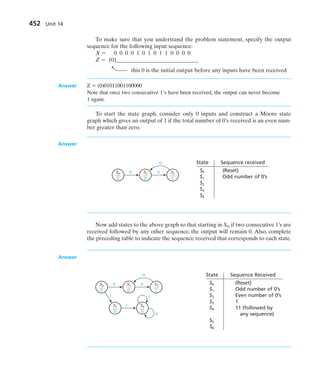


![Reduction of State Tables State Assignment 467
1. Study Section 15.1, Elimination of Redundant States.
2. Study Section 15.2, Equivalent States.
(a) State in words the meaning of 1(p, X) 2(q, X).
(b) Assuming that N1 and N2 are identical circuits with the following state
graph, use Definition 15.1 to show that p is not equivalent to q. [Calculate
(p, X) and (q, X) for X 0, X 1, X 00, X 01, etc.]
(c) Suppose you were given two sequential circuits (N1 and N2) in black boxes
with only input and output terminals available. Each box has a reset button.
The button on N1 resets it to state p and the button on N2 resets it to state q.
Could you experimentally determine if p q using Definition 15.1? Explain.
(d) Apply Theorem 15.1 to show that in Table 15-6, S2 [ S3.
(e) Note the difference between the definition of state equivalence
(Definition 15.1) and the state equivalence theorem (Theorem 15.1). The
definition requires an examination of output sequences but not next states,
while the theorem requires looking at both the output and next state for
each single input. Make sure that you know both the definition and the
theorem. Write out the definition of equivalent states:
Write out the state equivalence theorem:
When you check your answers,note that the theorem requires equal outputs
and equivalent next states. This distinction between equal and equivalent is
very important. For example, in the following state table, no two states have
equal next states, but we can still reduce the table to two states, because
r q
p
1
1
1
0
1
0
0
0
0
0
0
0
Study Guide](https://image.slidesharecdn.com/fundamentalsoflogicdesign6thcharlesh-240226091353-b43ce575/85/Fundamentals-of-Logic-Design-6th-Charles-H-Roth-pdf-490-320.jpg)


![482 Unit 15
Because the outputs of A and S2 correspond, the only possibility is A K S2. If we assume
that A K S2,this implies that we must have B K S0 which in turn implies that we must have
D K S1 and C K S3. Using the state tables, we can verify that these assumptions are cor-
rect because for every pair of assumed equivalent states, the next states are equivalent
and the outputs are equal when X K 0 and also when X K 1.This verifies that N1 K N2.
The implication table can easily be adapted for determining the equivalence of
sequential circuits. Because the states of one circuit must be checked for equivalence
against states of the other circuit, an implication chart is constructed with rows corre-
sponding to states of one circuit and columns corresponding to states of the other. For
example, for the circuits of Figure 15-6 we can set up the implication table of Figure
15-7(a).The first column of Figure 15-7(a) is filled in by comparing row A of the state
table in Figure 15-6(a) with each of the rows in Figure 15-6(b). Because states A and
S0 have different outputs, an X is placed in the A-S0 square. Because states A and S1
have the same outputs, the implied next-state pairs (B-S3 and A-S0) are placed in the
A-S1 square, etc.The remainder of the table is filled in similarly.
In the next step [Figure 15-7(b)], squares corresponding to additional nonequiv-
alent state pairs are crossed out. Thus, square A-S1 is crossed out because A [ S0.
Similarly, square B-S3 is crossed out because C [ S2, square C-S0 because A [ S3, and
S2
S0
S1
S3
1
0
1
0
0
0
0
0
0
0
0
0
1
1
1
1 C
A
D
B
1
0
0
0
0
0
0
0
0
0
1
1
1
1
1
1
(b)
(a)
FIGURE 15-6
Tables and Graphs
for Equivalent
Circuits
FIGURE 15-7
Implication Tables
for Determining
Circuit Equivalence
N1
X 0 1 X 0 1
A B A 0 0
B C D 0 1
C A C 0 1
D C B 0 0
N2
X 0 1 X 0 1
S0 S3 S1 0 1
S1 S3 S0 0 0
S2 S0 S2 0 0
S3 S2 S3 0 1
A B C D
S0
S1
S2
S3
A–S3
C–S1
C–S3
D–S1
B–S3
A–S0
B–S0
A–S2
C–S0
B–S2
C–S2
D–S3
A–S2
C–S3
C–S3
B–S0
A B C D
S0
S1
S2
S3
A–S3
C–S1
C–S3
D–S1
B–S3
A–S0
B–S0
A–S2
C–S0
B–S2
C–S2
D–S3
A–S2
C–S3
C–S3
B–S0
(a) (b)](https://image.slidesharecdn.com/fundamentalsoflogicdesign6thcharlesh-240226091353-b43ce575/85/Fundamentals-of-Logic-Design-6th-Charles-H-Roth-pdf-505-320.jpg)


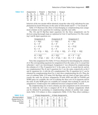


![Reduction of State Tables State Assignment 493
X X
00 01 11 10
00
BC
S1 S2
S1 S5 S2 S4
S1 S5 S2 S6
S1 S3 S2 S6
XA
01
11
10
Adjacent because S1, S3, and
S5 have adjacent
assignments
Adjacent because S4 and
S6 have adjacent
assignments
Adjacent because S3 and S5
have adjacent assignments
Adjacent because S0, S2, S4, and S6
have adjacent assignments
(a) Next-state maps for Figure 15-14
(b) Next-state maps for Figure 15-14 (cont.)
1 X X 1
00 01 11 10
1 0 0 1
1 0 0 1
1
00
01
11
10 1 0 1
0 X X 1
00 01 11 10
0 1 1 1
0 1 1 0
0
00
01
11
10 1 1 0
1 X X 0
00 01 11 10
1 1 0 0
1 1 0 0
1
00
BC
XA
A+ = DA = X′ B+ = DB = X′C′ + A′C + A′B C+ = DC = A + XB′
01
11
10 1 0 0
These pairs are adjacent because S2
and S5 have adjacent assignments
FIGURE 15-15 Next-State Maps for Figure 15-14
Next, we will apply the state assignment guidelines to Figure 15-16(a). First, we
list the sets of adjacent states specified by each Guideline:
1. (b, d) (c, f ) (b, e)
2. (a, c)2x (d, f ) (b, d) (b, f ) (c, e)
3. (a, c) (b, d) (e, f )
Next, we try to arrange the states on a map so as to satisfy as many of these pairs
as possible, but giving preference to the duplicated pairs (b, d) and (a, c). Two such
arrangements and the corresponding assignments are given in Figures 15-16(b) and
(c). For Figure 15-16(c), all adjacencies are satisfied except (b, f ), (c, e), and (e, f ).
We will derive D flip-flop input equations for this assignment. First, we construct the
transition table (Table 15-12) from the state table [Figure 15-16(a)] by replacing a
with 100, b with 111, c with 000, etc. Then, we plot the next-state and output maps](https://image.slidesharecdn.com/fundamentalsoflogicdesign6thcharlesh-240226091353-b43ce575/85/Fundamentals-of-Logic-Design-6th-Charles-H-Roth-pdf-516-320.jpg)


![15.37 Consider the following Mealy sequential circuit.
Present Next State Present Output
State X 0 X 1 X 0 X 1
A B A 0 0
B C A 0 0
C D A 0 1
D D A 0 0
(a) Use a one-hot state assignment, and implement the circuit using D flip-flops.
(b) Use the state assignment A 00, B 01, C 11, and D 10, and implement
the circuit using D flip-flops.
(c) Implement the circuit using a 4-bit parallel loading counter instead of flip-flops
for memory. Assume the synchronous counter controls are as follows:
s1 s0 Function
0 0 Hold
0 1 Increment
1 0 Parallel load
1 1 Clear
Q3Q2Q1Q0 are the outputs; P3P2P1P0 are the parallel inputs; and Q0 is the least
significant bit of the counter. (With the proper state assignment, this can be
done without using the parallel load function of the counter.)
(d) Implement the circuit using a 4-bit parallel loading shift register instead of
flip-flops for memory. Assume the synchronous shift register controls are as
follows:
s1 s0 Function
0 0 Hold
0 1 Shift right
1 0 Parallel load
1 1 Clear
Sin is the input for the shift; Q3Q2Q1Q0 are the outputs; P3P2P1P0 are the parallel
inputs. When shifting, Sin → Q3, Q3 → Q2, Q2 → Q1, Q1 → Q0. (With the proper
state assignment, this can be done without using the parallel load function of the
shift register.)
15.38 A sequential circuit contains two D flip-flops; the excitation equations for the flip-
flops are D1 XQ1 XQ2 and D2 XQ1 XQ2
(a) Convert the circuit into an equivalent one where each D flip-flop is replaced by
a T flip-flop. Do this by converting the next-state equations into the form for a
T flip-flop. [Hint: MQ NQ (M Q NQ ) Q (M Q NQ )Q .]
(b) Repeat Part (a) by constructing an excitation table for the T flip-flops, i.e., a
truth table for T1 and T2 as a function of X, Q1, and Q2.
(c) Convert the circuit into an equivalent one where each D flip-flop is replaced by
a J-K flip-flop. Do this by converting the next-state equations into the form
for a J-K flip-flop.
Reduction of State Tables State Assignment 509](https://image.slidesharecdn.com/fundamentalsoflogicdesign6thcharlesh-240226091353-b43ce575/85/Fundamentals-of-Logic-Design-6th-Charles-H-Roth-pdf-532-320.jpg)
![(d) Repeat Part (c) by constructing an excitation table for the J-K flip-flops, i.e., a
truth table for the J and K flip-flop inputs as a function of X, Q1, and Q2.
15.39 A sequential circuit contains two J-K flip-flops; the excitation equations for the flip-
flops are J1 Q2, K1 Q1, J2 X Q1 , and K2 1.
(a) Convert the circuit into an equivalent one where each J-K flip-flop is replaced
by a T flip-flop. Do this by converting the next-state equations into the form for
a T flip-flop. [Hint: MQ NQ (M Q NQ ) Q (M Q NQ )Q .]
(b) Repeat Part (a) by constructing an excitation table for the T flip-flops, i.e., a
truth table for T1 and T2 as a function of X, Q1, and Q2.
(c) Convert the circuit into an equivalent one where each D flip-flop is replaced by
an S-R flip-flop. Do this by converting the next-state equations into the form for
a S-R flip-flop.
(d) Repeat Part (c) by constructing an excitation table for the S-R flip-flops, i.e., a
truth table for the S and R flip-flop inputs as a function of X, Q1, and Q2.
510 Unit 15](https://image.slidesharecdn.com/fundamentalsoflogicdesign6thcharlesh-240226091353-b43ce575/85/Fundamentals-of-Logic-Design-6th-Charles-H-Roth-pdf-533-320.jpg)


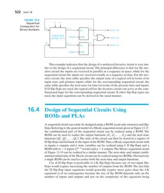


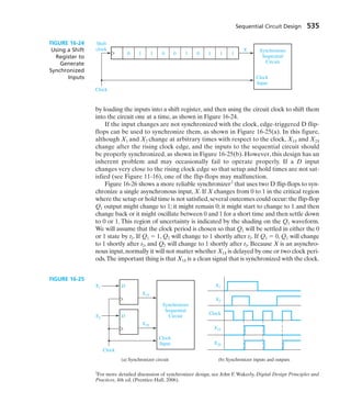


![(c) Design a Moore sequential circuit using T flip-flops to do the same task, show-
ing a state graph and input equations for a reasonably economical design.
16.19 Design a sequential circuit to multiply an 8-4-2-1 binary-coded decimal digit by 3 to
give a 5-bit binary number. For example, if the input is 0111, the output should be
10101. The input and output to the circuit should be serial with the least significant
bit first. Assume that the input will be 0 at the fifth clock time and reset the circuit
after the fifth output bit. [Hint: As each bit is received, multiply it by 3, giving a
product of either 00 or 11. Thus we either output 0 and carry 0 to the next column,
or output 1 and carry 1 to the next column. If we carry a 1 to the next column, then
the sum of the carry and the next product is either 01 or 100. In this case, we either
output 1 and carry 0 or output 0 and carry 10 (2) to the next column.What happens
if we carry 10 (2) to the next column?]
(a) Derive a state table with a minimum number of states (3 states).
(b) Design the circuit using J-K flip-flops and NAND and NOR gates.
(c) Design the circuit using a PLA and D flip-flops. Give the PLA table.
16.20 A Moore sequential circuit has three inputs (X2, X1, and X0) that specify a temper-
ature range in a room. The circuit has two outputs (I and D) that control a heater
for the room; I 1 causes the heater to increase its heat output, and D 1 causes
the heater to decrease its heat output. If the temperature range is 0, 1, or 2 for three
successive clock cycles, the circuit generates I 1, and conversely if the temperature
range is 5, 6, or 7 for three successive clock cycles, the circuit generates D 1;
otherwise, I 0 and D 0.
(a) Construct a state diagram for the circuit.
(b) Encode the states using a one-hot state assignment and derive the D flip-flop
input equations and the output equations.
(c) Use a minimum number of D flip-flops and derive the D flip-flop input equa-
tions and the output equations.
16.21 Repeat Problem 16.20 using a Mealy circuit.
16.22 A Moore sequential circuit has two inputs (X and Y) and three outputs (Z2, Z1, and
Z0). The outputs are a 1’s complement number specifying the number of successive
times X and Y have been equal or not equal as follows: In decimal, the outputs are
1, 2, and 3 if X and Y have been equal for one time, two successive times, and three
or more successive times, and the outputs are, 1, 2, and 3 if X and Y have been
not equal for one time, two successive times, and three or more successive times.
Initially, the outputs are all 0.
(a) Construct a state diagram for the circuit.
(b) Encode the states using a one-hot state assignment and derive the D flip-flop
input equations and the output equations.
(c) Use a minimum number of D flip-flops and derive the D flip-flop input equa-
tions and the output equations.
16.23 Repeat Problem 16.22 using a Mealy sequential circuit.
Sequential Circuit Design 545](https://image.slidesharecdn.com/fundamentalsoflogicdesign6thcharlesh-240226091353-b43ce575/85/Fundamentals-of-Logic-Design-6th-Charles-H-Roth-pdf-568-320.jpg)


![The condition is a Boolean expression which evaluates to TRUE or FALSE. If it is
TRUE, sequential statements1 are executed; otherwise, sequential statements2 are
executed. VHDL if statements are sequential statements that can be used within a
process, but they cannot be used as concurrent statements outside of a process. On
the other hand, conditional signal assignment statements are concurrent statements
that cannot be used within a process.
The most general form of the if statement is
if condition then
sequential statements
{elsif condition then
sequential statements}
-- 0 or more elsif clauses may be included
[else sequential statements]
end if;
The curly brackets indicate that any number of elsif clauses may be included, and the
square brackets indicate that the else clause is optional. The example of Figure 17-4
shows how a flow chart can be represented using nested ifs or the equivalent using
elsifs. In this example, C1, C2, and C3 represent conditions that can be TRUE or
FALSE, and S1, S2, . . . S8 represent sequential statements. Each if requires a corre-
sponding end if, but an elsif does not.
Next, we will write a VHDL module for a J-K flip-flop (Figure 17-5). This flip-
flop has active-low asynchronous preset (SN) and clear (RN) inputs. State changes
related to J and K occur on the falling edge of the clock. In this chapter, we use a
suffix N to indicate an active-low (negative-logic) signal. For simplicity, we will
assume that the condition SN RN 0 does not occur.
556 Unit 17
FIGURE 17-4
Equivalent
Representations
of a Flow Chart
Using Nested
Ifs and Elsifs
C1
T
S1; S2; C2
T
S3; S4; C3
T
F
F
F
S5; S6; S7; S8;
if (C1) then S1; S2;
else if (C2) then S3; S4;
else if (C3) then S5; S6;
else S7; S8;
end if;
end if;
end if;
if (C1) then S1; S2;
elsif (C2) then S3; S4;
elsif (C3) then S5; S6;
else S7; S8;
end if;](https://image.slidesharecdn.com/fundamentalsoflogicdesign6thcharlesh-240226091353-b43ce575/85/Fundamentals-of-Logic-Design-6th-Charles-H-Roth-pdf-579-320.jpg)

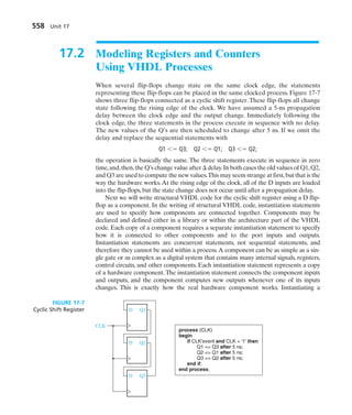


![VHDL for Sequential Logic 565
The case statement has the general form:
case expression is
when choice1 sequential statements1
when choice2 sequential statements2
. . .
[when others sequential statements]
end case;
The “expression” is evaluated first. If it is equal to “choice1”, then “sequential
statements1” are executed; if it is equal to “choice2”, then “sequential state-
ments2” are executed, etc. All possible values of the expression must be included
in the choices. If all values are not explicitly given, a “when others” clause is
required in the case statement. If no action is specified for the other choices, the
clause should be
when others null;
17.4 Modeling a Sequential Machine
In this section we will discuss several ways of writing VHDL descriptions for
sequential machines. First, we will write a behavioral model for a Mealy sequential
circuit based on the state table of Table 17-2. This table is the same as Table 16-3
with the states renamed. It represents a BCD to excess-3 code converter with
inputs and outputs LSB first.
As shown in Figure 17-16, a Mealy machine consists of a combinational cir-
cuit and a state register. The VHDL model of Figure 17-17 uses two processes to
represent these two parts of the circuit. Because X and Z are external signals, they
are declared in the port. State and Nextstate are internal signals that represent the
state and next state of the sequential circuit, so they are declared at the start of the
architecture.At the behavioral level, we represent the state and next state of the cir-
cuit by integer signals with a range of 0 to 6.
NS Z
PS X 0 X 1 X 0 X 1
S0 S1 S2 1 0
S1 S3 S4 1 0
S2 S4 S4 0 1
S3 S5 S5 0 1
S4 S5 S6 1 0
S5 S0 S0 0 1
S6 S0 – 1 –
TABLE 17-2
State Table for
Code Converter](https://image.slidesharecdn.com/fundamentalsoflogicdesign6thcharlesh-240226091353-b43ce575/85/Fundamentals-of-Logic-Design-6th-Charles-H-Roth-pdf-588-320.jpg)


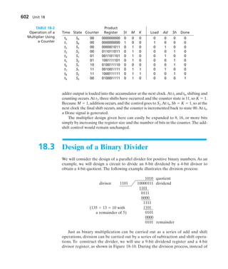


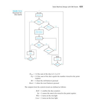


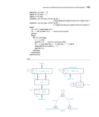


Fundamentals of Logic Design 6th Charles H.Roth.pdf
- 3. This page intentionally left blank
- 4. Charles H. Roth, Jr. University of Texas at Austin Larry L. Kinney University of Minnesota, Twin Cities Fundamentals of Logic Design Australia • Brazil • Japan • Korea • Mexico • Singapore • Spain • United Kingdom • United States
- 5. Director, Global Engineering Program: Chris Carson Senior Developmental Editor: Hilda Gowans Editorial Assistant: Jennifer Dismore Marketing Services Coordinator: Lauren Bestos Director, Content and Media Production: Barbara Fuller-Jacobsen Content Project Manager: Cliff Kallemeyn Production Service: RPK Editorial Services, Inc. Copyeditor: Fred Dahl Proofreader: Harlan James Indexer: Ron Prottsman Compositor: Integra Senior Art Director: Michelle Kunkler Internal Designer: Carmela Periera Cover Designer: Andrew Adams Cover Image: © Shutterstock/guattièro boffi Senior First Print Buyer: Doug Wilke Printed in the United States of America 1 2 3 4 5 6 7 12 11 10 09 08 Fundamentals of Logic Design, Sixth Edition Charles H. Roth, Jr. and Larry L. Kinney © 2010 and 2004 Cengage Learning ALL RIGHTS RESERVED. No part of this work covered by the copyright herein may be reproduced, transmitted, stored, or used in any form or by any means—graphic, electronic, or mechanical, including but not limited to photocopying, recording, scanning, digitizing, taping,Web distribution, information networks, information storage and retrieval systems, or in any other manner—except as may be permitted by the license terms herein. For product information and technology assistance, contact us at Cengage Learning Customer & Sales Support, 1-800-354-9706. For permission to use material from this text or product, submit all requests online at www.cengage.com/permissions. Further permissions questions can be emailed to [email protected]. Library of Congress Control Number: 2009920814 Student Edition with CD: ISBN-13: 978-0-495-47169-1 ISBN-10: 0-495-47169-0 Student Edition: ISBN-13: 978-0-495-66804-6 ISBN-10: 0-495-66804-4 Cengage Learning 200 First Stamford Place, Suite 400 Stamford, CT 06902 USA Cengage Learning is a leading provider of customized learning solutions with office locations around the globe, including Singapore, the United Kingdom,Australia, Mexico, Brazil, and Japan. Locate your local office at: international.cengage.com/region. Cengage Learning products are represented in Canada by Nelson Education Ltd. For your course and learning solutions, visit www.cengage.com/engineering. Purchase any of our products at your local college store or at our preferred online store www.ichapters.com.
- 6. Introduction 1 Number Systems and Conversion 1 2 Boolean Algebra 27 3 Boolean Algebra (Continued) 56 Applications of Boolean Algebra 4 Minterm and Maxterm Expansions 83 5 Karnaugh Maps 116 6 Quine-McCluskey Method 159 Multi-Level Gate Circuits 7 NAND and NOR Gates 184 Combinational Circuit Design 8 and Simulation Using Gates 215 Multiplexers, Decoders, and Programmable 9 Logic Devices 242 Brief Contents
- 7. 10 Introduction to VHDL 280 11 Latches and Flip-Flops 317 12 Registers and Counters 348 13 Analysis of Clocked Sequential Circuits 388 14 Derivation of State Graphs and Tables 427 Reduction of State Tables 15 State Assignment 466 16 Sequential Circuit Design 511 17 VHDL for Sequential Logic 549 18 Circuits for Arithmetic Operations 591 19 State Machine Design with SM Charts 623 20 VHDL for Digital System Design 646 A Appendices 675 vi Brief Contents
- 8. vii Preface xv How to Use This Book for Self-Study xix Unit 1 Introduction Number Systems and Conversion Objectives 1 Study Guide 2 1.1 Digital Systems and Switching Circuits 6 1.2 Number Systems and Conversion 8 1.3 Binary Arithmetic 12 1.4 Representation of Negative Numbers 16 Addition of 2’s Complement Numbers 17 Addition of 1’s Complement Numbers 19 1.5 Binary Codes 21 Problems 23 Unit 2 Boolean Algebra Objectives 27 Study Guide 28 2.1 Introduction 34 2.2 Basic Operations 35 2.3 Boolean Expressions and Truth Tables 37 2.4 Basic Theorems 39 2.5 Commutative,Associative, and Distributive Laws 40 2.6 Simplification Theorems 42 2.7 Multiplying Out and Factoring 44 Contents
- 9. 2.8 DeMorgan’s Laws 47 Problems 48 Laws and Theorems of Boolean Algebra 55 Unit 3 Boolean Algebra (Continued) Objectives 56 Study Guide 57 3.1 Multiplying Out and Factoring Expressions 62 3.2 Exclusive-OR and Equivalence Operations 64 3.3 The Consensus Theorem 66 3.4 Algebraic Simplification of Switching Expressions 68 3.5 Proving Validity of an Equation 70 Programmed Exercises 73 Problems 78 Unit 4 Applications of Boolean Algebra Minterm and Maxterm Expansions Objectives 83 Study Guide 84 4.1 Conversion of English Sentences to Boolean Equations 90 4.2 Combinational Logic Design Using a Truth Table 92 4.3 Minterm and Maxterm Expansions 93 4.4 General Minterm and Maxterm Expansions 96 4.5 Incompletely Specified Functions 99 4.6 Examples of Truth Table Construction 100 4.7 Design of Binary Adders and Subtracters 104 Problems 107 Unit 5 Karnaugh Maps Objectives 116 Study Guide 117 5.1 Minimum Forms of Switching Functions 127 5.2 Two- and Three-Variable Karnaugh Maps 129 5.3 Four-Variable Karnaugh Maps 133 5.4 Determination of Minimum Expressions Using Essential Prime Implicants 136 5.5 Five-Variable Karnaugh Maps 141 5.6 Other Uses of Karnaugh Maps 144 viii Contents
- 10. 5.7 Other Forms of Karnaugh Maps 146 Programmed Exercises 147 Problems 152 Unit 6 Quine-McCluskey Method Objectives 159 Study Guide 160 6.1 Determination of Prime Implicants 165 6.2 The Prime Implicant Chart 168 6.3 Petrick’s Method 171 6.4 Simplification of Incompletely Specified Functions 173 6.5 Simplification Using Map-Entered Variables 174 6.6 Conclusion 176 Programmed Exercise 177 Problems 181 Unit 7 Multi-Level Gate Circuits NAND and NOR Gates Objectives 184 Study Guide 185 7.1 Multi-Level Gate Circuits 190 7.2 NAND and NOR Gates 195 7.3 Design of Two-Level NAND- and NOR- Gate Circuits 197 7.4 Design of Multi-Level NAND- and NOR- Gate Circuits 200 7.5 Circuit Conversion Using Alternative Gate Symbols 201 7.6 Design of Two-Level, Multiple-Output Circuits 204 Determination of Essential Prime Implicants for Multiple-Output Realization 206 7.7 Multiple-Output NAND- and NOR-Gate Circuits 208 Problems 208 Unit 8 Combinational Circuit Design and Simulation Using Gates Objectives 215 Study Guide 216 8.1 Review of Combinational Circuit Design 219 8.2 Design of Circuits with Limited Gate Fan-In 220 8.3 Gate Delays and Timing Diagrams 222 Contents ix
- 11. 8.4 Hazards in Combinational Logic 224 8.5 Simulation and Testing of Logic Circuits 229 Problems 232 Design Problems 236 Unit 9 Multiplexers, Decoders, and Programmable Logic Devices Objectives 242 Study Guide 243 9.1 Introduction 250 9.2 Multiplexers 251 9.3 Three-State Buffers 253 9.4 Decoders and Encoders 256 9.5 Read-Only Memories 259 9.6 Programmable Logic Devices 263 Programmable Logic Arrays 263 Programmable Array Logic 266 9.7 Complex Programmable Logic Devices 268 9.8 Field-Programmable Gate Arrays 270 Decomposition of Switching Functions 271 Problems 274 Unit 10 Introduction to VHDL Objectives 280 Study Guide 281 10.1 VHDL Description of Combinational Circuits 285 10.2 VHDL Models for Multiplexers 290 10.3 VHDL Modules 292 Four-Bit Full Adder 294 10.4 Signals and Constants 297 10.5 Arrays 298 10.6 VHDL Operators 301 10.7 Packages and Libraries 302 10.8 IEEE Standard Logic 304 10.9 Compilation and Simulation of VHDL Code 307 Problems 308 Design Problems 313 x Contents
- 12. Unit 11 Latches and Flip-Flops Objectives 317 Study Guide 318 11.1 Introduction 322 11.2 Set-Reset Latch 323 11.3 Gated D Latch 327 11.4 Edge-Triggered D Flip-Flop 328 11.5 S-R Flip-Flop 331 11.6 J-K Flip-Flop 332 11.7 T Flip-Flop 333 11.8 Flip-Flops with Additional Inputs 334 11.9 Summary 336 Problems 337 Programmed Exercise 345 Unit 12 Registers and Counters Objectives 348 Study Guide 349 12.1 Registers and Register Transfers 354 Parallel Adder with Accumulator 356 12.2 Shift Registers 358 12.3 Design of Binary Counters 362 12.4 Counters for Other Sequences 367 Counter Design Using D Flip-Flops 370 12.5 Counter Design Using S-R and J-K Flip-Flops 371 12.6 Derivation of Flip-Flop Input Equations—Summary 374 Problems 378 Unit 13 Analysis of Clocked Sequential Circuits Objectives 388 Study Guide 389 13.1 A Sequential Parity Checker 395 13.2 Analysis by Signal Tracing and Timing Charts 397 13.3 State Tables and Graphs 401 Construction and Interpretation of Timing Charts 406 Contents xi
- 13. 13.4 General Models for Sequential Circuits 408 Programmed Exercise 412 Problems 416 Unit 14 Derivation of State Graphs and Tables Objectives 427 Study Guide 428 14.1 Design of a Sequence Detector 431 14.2 More Complex Design Problems 435 14.3 Guidelines for Construction of State Graphs 439 14.4 Serial Data Code Conversion 444 14.5 Alphanumeric State Graph Notation 448 Programmed Exercises 449 Problems 456 Unit 15 Reduction of State Tables State Assignment Objectives 466 Study Guide 467 15.1 Elimination of Redundant States 474 15.2 Equivalent States 476 15.3 Determination of State Equivalence Using an Implication Table 478 15.4 Equivalent Sequential Circuits 481 15.5 Incompletely Specified State Tables 483 15.6 Derivation of Flip-Flop Input Equations 484 15.7 Equivalent State Assignments 487 15.8 Guidelines for State Assignment 490 15.9 Using a One-Hot State Assignment 495 Problems 498 Unit 16 Sequential Circuit Design Objectives 511 Study Guide 512 16.1 Summary of Design Procedure for Sequential Circuits 514 16.2 Design Example—Code Converter 515 16.3 Design of Iterative Circuits 519 Design of a Comparator 519 xii Contents
- 14. 16.4 Design of Sequential Circuits Using ROMs and PLAs 522 16.5 Sequential Circuit Design Using CPLDs 525 16.6 Sequential Circuit Design Using FPGAs 529 16.7 Simulation and Testing of Sequential Circuits 531 16.8 Overview of Computer-Aided Design 536 Design Problems 538 Additional Problems 544 Unit 17 VHDL for Sequential Logic Objectives 549 Study Guide 550 17.1 Modeling Flip-Flops Using VHDL Processes 554 17.2 Modeling Registers and Counters Using VHDL Processes 558 17.3 Modeling Combinational Logic Using VHDL Processes 563 17.4 Modeling a Sequential Machine 565 17.5 Synthesis of VHDL Code 572 17.6 More About Processes and Sequential Statements 575 Problems 577 Simulation Problems 588 Unit 18 Circuits for Arithmetic Operations Objectives 591 Study Guide 592 18.1 Serial Adder with Accumulator 594 18.2 Design of a Parallel Multiplier 598 18.3 Design of a Binary Divider 602 Programmed Exercises 607 Problems 612 Unit 19 State Machine Design with SM Charts Objectives 623 Study Guide 624 19.1 State Machine Charts 625 19.2 Derivation of SM Charts 630 19.3 Realization of SM Charts 635 Problems 640 Contents xiii
- 15. Unit 20 VHDL for Digital System Design Objectives 646 Study Guide 647 20.1 VHDL Code for a Serial Adder 650 20.2 VHDL Code for a Binary Multiplier 652 20.3 VHDL Code for a Binary Divider 662 20.4 VHDL Code for a Dice Game Simulator 664 20.5 Concluding Remarks 667 Problems 668 Lab Design Problems 671 A Appendices A MOS and CMOS Logic 675 B VHDL Language Summary 681 C Tips for Writing Synthesizable VHDL Code 686 D Proofs of Theorems 689 E Answers to Selected Study Guide Questions and Problems 691 References 747 Index 748 xiv Contents
- 16. Contents xv After studying this text, you should be able to apply switching theory to the solution of logic design problems.This means that you will learn both the basic theory of switching circuits and how to apply it.After a brief introduction, you will study Boolean algebra, which is the basic mathematical tool needed to analyze and synthesize an important class of switching circuits. Starting from a problem statement, you will learn to design circuits of logic gates that have a specified relationship between signals at the input and output terminals.Then you will study the logical properties of flip-flops, which serve as memory devices in sequential switching circuits.By combining flip-flops with circuits of logic gates,you will learn to design counters,adders,sequence detectors,and similar cir- cuits.You will also study the VHDL hardware description language and its application to the design of combinational logic, sequential logic, and simple digital systems. The fifth edition offers a number of improvements over the fourth edition.Material in the text has been reorganized to provide a better teaching sequence, and obsolete material has been removed.The chapter on latches and flip-flops has been rewritten. Greater emphasis is placed on the use of programmable logic devices (PLDs), includ- ing programmable gate arrays and complex PLDs. New exercises and problems have been added to every unit, and several sections have been rewritten to clarify the pres- entation. Three chapters on the VHDL hardware description language have been added, and more emphasis is placed on the role of simulation and computer-aided design of logic circuits. This text is designed so that it can be used in either a standard lecture course or in a self-paced course. In addition to the standard reading material and problems, study guides and other aids for self-study are included in the text.The content of the text is divided into 20 study units. These units form a logical sequence so that mas- tery of the material in one unit is generally a prerequisite to the study of succeeding units. Each unit consists of four parts. First, a list of objectives states precisely what you are expected to learn by studying the unit. Next, the study guide contains read- ing assignments and study questions.As you work through the unit, you should write out the answers to these study questions.The text material and problem set that fol- low are similar to a conventional textbook. When you complete a unit, you should review the objectives and make sure that you have met them. Preface xv
- 17. The study units are divided into three main groups.The first 9 units treat Boolean algebra and the design of combinational logic circuits. Units 11 through 16, 18 and 19 are mainly concerned with the analysis and design of clocked sequential logic cir- cuits, including circuits for arithmetic operations. Units 10, 17, and 20 introduce the VHDL hardware description language and its application to logic design. Since the computer plays an important role in the logic design process, integra- tion of computer usage into the first logic design course is very important. A com- puter-aided logic design program, called LogicAid, is included on the CD provided with this textbook.LogicAid allows the student easily to derive simplified logic equa- tions from minterms, truth tables, and state tables. This relieves the student of some of the more tedious computations and permits the solution of more complex design problems in a shorter time. LogicAid also provides tutorial help for Karnaugh maps and derivation of state graphs. Several of the units include simulation or laboratory exercises. These exercises provide an opportunity to design a logic circuit and then test its operation. The SimUaid logic simulator, provided on the CD, may be used to verify the logic designs. The lab equipment required for testing either can be a breadboard with integrated circuit flip-flops and logic gates or a circuit board with a programmable logic device. If such equipment is not available, the lab exercises can be simulated with SimUaid or just assigned as design problems. This is especially important for Units 8, 16, and 20 because the comprehensive design problems in these units help to review and tie together the material in several of the preceding units. As integrated circuit technology continues to improve to allow more components on a chip,digital systems continue to grow in complexity.Design of such complex sys- tems is facilitated by the use of a hardware description language such as VHDL.This text introduces the use of VHDL in logic design and emphasizes the relationship between VHDL statements and the corresponding digital hardware. VHDL allows digital hardware to be described and simulated at a higher level before it is imple- mented with logic components. Computer programs for synthesis can convert a VHDL description of a digital system to a corresponding set of logic components and their interconnections. Even though use of such computer-aided design tools helps to automate the logic design process, we believe that it is important to under- stand the underlying logic components and their timing before writing VHDL code. By first implementing the digital logic manually, students more fully can appreciate the power and limitations of VHDL. This text is written for a first course in the logic design of digital systems.It is writ- ten on the premise that the student should understand and learn thoroughly certain fundamental concepts in a first course. Examples of such fundamental concepts are the use of Boolean algebra to describe the signals and interconnections in a logic cir- cuit, use of systematic techniques for simplification of a logic circuit, interconnection of simple components to perform a more complex logic function, analysis of a sequential logic circuit in terms of timing charts or state graphs, and use of a control circuit to control the sequence of events in a digital system. The text attempts to achieve a balance between theory and application. For this reason, the text does not overemphasize the mathematics of switching theory; how- ever, it does present the theory that is necessary for understanding the fundamental xvi Preface
- 18. concepts of logic design. After completing this text, the student should be prepared for a more advanced digital systems design course that stresses more intuitive con- cepts like the development of algorithms for digital processes, partitioning of digital systems into subsystems, and implementation of digital systems using currently avail- able hardware. Alternatively, the student should be prepared to go on to a more advanced course in switching theory that further develops the theoretical concepts that have been introduced here. Although the technology used to implement digital systems has changed signifi- cantly since the first edition of this text was published, the fundamental principles of logic design have not. Truth tables and state tables still are used to specify the behavior of logic circuits, and Boolean algebra is still a basic mathematical tool for logic design. Even when programmable logic devices are used instead of individual gates and flip-flops, reduction of logic equations is still desirable in order to fit the equations into smaller PLDs. Making a good state assignment is still desirable, because without a good assignment, the logic equations may require larger PLDs. The text is suitable for both computer science and engineering students. Material relating to circuit aspects of logic gates is contained in Appendix A so that this material can conveniently be omitted by computer science students or other students with no background in electronic circuits.The text is organized so that Unit 6 on the Quine-McCluskey procedure may be omitted without loss of continuity. The three units on VHDL can be studied in the normal sequence, studied together after the other units, or omitted entirely. Although many texts are available in the areas of switching theory and logic design, this text was originally developed to meet the needs of a self-paced course in which students are expected to study the material on their own. Each of the units has undergone extensive class testing in a self-paced environment and has been revised based on student feedback. Study guides and text material have been expanded as required so that students can learn from the text without the aid of lectures and so that almost all of the students can achieve mastery of all of the objectives. Supplementary materials were developed as the text was being written.An instructor’s manual is available that includes sugges- tions for using the text in a standard or self-paced course, quizzes on each of the units, and suggestions for laboratory equipment and procedures. The instructor’s manual also contains solutions to problems, to unit quizzes, and to lab exercises. To be effective, a book designed for self-study cannot simply be written. It must be tested and revised many times to achieve its goals. I wish to express my apprecia- tion to the many professors, proctors, and students who participated in this process. Special thanks go to Dr. David Brown, who worked with me in teaching the self- paced course, and who made many helpful suggestions for improving the text. I am especially grateful to graduate teaching assistant, Mark Story, who developed many new problems and solutions for the fifth edition and who offered many suggestions for improving the consistency and clarity of the presentation. Charles H. Roth, Jr. Preface xvii
- 19. The major change in the sixth edition of the text is the addition of over 150 new prob- lems and the modification of several of the fifth edition problems.Substantial new dis- cussion was added to the units on VHDL. Other topics receiving expanded discussion are hazards, latches and one-hot state assignments. In addition, the logic design and simulation software that accompanies the text has been updated and improved. Larry L. Kinney Charles H. Roth, Jr. Preface to the Sixth Edition xviii
- 20. If you wish to learn all of the material in this text to mastery level, the following study procedures are recommended for each unit: 1. Read the Objectives of the unit. These objectives provide a concise summary of what you should be able to do when you complete study of the unit. 2. Work through the Study Guide.After reading each section of the text,write out the answers to the corresponding study guide questions.In many cases,blank spaces are left in the study guide so that you can write your answers directly in this book. By doing this, you will have the answers conveniently available for later review. The study guide questions generally will help emphasize some of the important points in each section or will guide you to a better understanding of some of the more dif- ficult points. If you cannot answer some of the study guide questions, this indicates that you need to study the corresponding section in the text more before proceed- ing.The answers to selected study guide questions are given in the back of this book; answers to the remaining questions generally can be found within the text. 3. Several of the units (Units 3, 5, 6, 11, 13, 14, and 18) contain one or more pro- grammed exercises. Each programmed exercise will guide you step-by-step through the solution of one of the more difficult types of problems encountered in this text. When working through a programmed exercise, be sure to write down your answer for each part in the space provided before looking at the an- swer and continuing with the next part of the exercise. 4. Work the assigned Problems at the end of the unit. Check your answers against those at the end of the book and rework any problems that you missed. 5. Reread the Objectives of the unit to make sure that you can meet all of them. If in doubt, review the appropriate sections of the text. 6. If you are using this text in a self-paced course, you will need to pass a readiness test on each unit before proceeding with the next unit. The purpose of the readi- ness test is to make sure that you have mastered the objectives of one unit before moving on to the next unit.The questions on the test will relate directly to the ob- jectives of the unit, so that if you have worked through the study guide and writ- ten out answers to all of the study guide questions and to the problems assigned in the study guide, you should have no difficulty passing the test. How to Use This Book for Self-Study xix
- 21. This page intentionally left blank
- 24. Introduction Number Systems and Conversion U N I T 1 Objectives 1. Introduction The first part of this unit introduces the material to be studied later. In addition to getting an overview of the material in the first part of the course, you should be able to explain a. The difference between analog and digital systems and why digital systems are capable of greater accuracy b. The difference between combinational and sequential circuits c. Why two-valued signals and binary numbers are commonly used in digital systems 2. Number systems and conversion When you complete this unit, you should be able to solve the following types of problems: a. Given a positive integer, fraction, or mixed number in any base (2 through 16); convert to any other base. Justify the procedure used by using a power series expansion for the number. b. Add, subtract, multiply, and divide positive binary numbers. Explain the addition and subtraction process in terms of carries and borrows. c. Write negative binary numbers in sign and magnitude, 1’s comple- ment, and 2’s complement forms. Add signed binary numbers using 1’s complement and 2’s complement arithmetic. Justify the methods used. State when an overflow occurs. d. Represent a decimal number in binary-coded-decimal (BCD), 6-3-1-1 code, excess-3 code, etc. Given a set of weights, construct a weighted code. 1
- 25. 1. Study Section 1.1, Digital Systems and Switching Circuits, and answer the fol- lowing study questions: (a) What is the basic difference between analog and digital systems? (b) Why are digital systems capable of greater accuracy than analog systems? (c) Explain the difference between combinational and sequential switching circuits. (d) What common characteristic do most switching devices used in digital systems have? (e) Why are binary numbers used in digital systems? 2. Study Section 1.2, Number Systems and Conversion. Answer the following study questions as you go along: (a) Is the first remainder obtained in the division method for base conversion the most or least significant digit? (b) Work through all of the examples in the text as you encounter them and make sure that you understand all of the steps. (c) An easy method for conversion between binary and hexadecimal is illus- trated in Equation (1-1). Why should you start forming the groups of four bits at the binary point instead of the left end of the number? (d) Why is it impossible to convert a decimal number to binary on a digit-by- digit basis as can be done for hexadecimal? 2 Unit 1 Study Guide
- 26. (e) Complete the following conversion table. Binary Octal Decimal Hexadecimal (base 2) (base 8) (base 10) (base 16) 0 0 0 0 1 10 11 100 101 110 111 1000 1001 1010 1011 1100 1101 1110 1111 10000 20 16 10 (f) Work Problems 1.1, 1.2, 1.3, and 1.4. 3. Study Section 1.3, Binary Arithmetic. (a) Make sure that you can follow all of the examples, especially the propaga- tion of borrows in the subtraction process. (b) To make sure that you understand the borrowing process, work out a detailed analysis in terms of powers of 2 for the following example: 1100 101 111 4. Work Problems 1.5, 1.6, and 1.17(a). 5. Study Section 1.4, Representation of Negative Numbers. (a) In digital systems, why are 1’s complement and 2’s complement commonly used to represent negative numbers instead of sign and magnitude? Number Systems and Conversion 3
- 27. (b) State two different ways of forming the 1’s complement of an n-bit binary number. (c) State three different ways of forming the 2’s complement of an n-bit binary number. (d) If the word length is n 4 bits (including sign), what decimal number does 10002 represent in sign and magnitude? In 2’s complement? In 1’s complement? (e) Given a negative number represented in 2’s complement, how do you find its magnitude? Given a negative number represented in 1’s complement, how do you find its magnitude? (f) If the word length is 6 bits (including sign), what decimal number does 1000002 represent in sign and magnitude? In 2’s complement? In 1’s complement? (g) What is meant by an overflow? How can you tell that an overflow has occurred when performing 1’s or 2’s complement addition? Does a carry out of the last bit position indicate that an overflow has occurred? 4 Unit 1
- 28. (h) Work out some examples of 1’s and 2’s complement addition for various combinations of positive and negative numbers. (i) What is the justification for using the end-around carry in 1’s complement addition? (j) The one thing that causes the most trouble with 2’s complement numbers is the special case of the negative number which consists of a 1 followed by all 0’s (1000 . . . 000). If this number is n bits long, what number does it rep- resent and why? (It is not negative zero.) (k) Work Problems 1.7 and 1.8. 6. Study Section 1.5, Binary Codes. (a) Represent 187 in BCD code,excess-3 code,6-3-1-1 code,and 2-out-of-5 code. (b) Verify that the 6-3-1-1 code is a weighted code. Note that for some decimal digits, two different code combinations could have been used. For example, either 0101 or 0110 could represent 4. In each case the combination with the smaller binary value has been used. (c) How is the excess-3 code obtained? (d) How are the ASCII codes for the decimal digits obtained? What is the rela- tion between the ASCII codes for the capital letters and lowercase letters? (e) Work Problem 1.9. 7. If you are taking this course on a self-paced basis, you will need to pass a readi- ness test on this unit before going on to the next unit.The purpose of the readi- ness test is to determine if you have mastered the material in this unit and are ready to go on to the next unit. Before you take the readiness test: (a) Check your answers to the problems against those provided at the end of this book. If you missed any of the problems, make sure that you under- stand why your answer is wrong and correct your solution. (b) Make sure that you can meet all of the objectives listed at the beginning of this unit. Number Systems and Conversion 5
- 29. Introduction Number Systems and Conversion 6 1.1 Digital Systems and Switching Circuits Digital systems are used extensively in computation and data processing, control systems, communications, and measurement. Because digital systems are capable of greater accuracy and reliability than analog systems, many tasks formerly done by analog systems are now being performed digitally. In a digital system, the physical quantities or signals can assume only discrete values, while in analog systems the physical quantities or signals may vary con- tinuously over a specified range. For example, the output voltage of a digital sys- tem might be constrained to take on only two values such as 0 volts and 5 volts, while the output voltage from an analog system might be allowed to assume any value in the range 10 volts to 10 volts. Because digital systems work with discrete quantities, in many cases they can be designed so that for a given input, the output is exactly correct. For example, if we multiply two 5-digit numbers using a digital multiplier, the 10-digit product will be correct in all 10 digits. On the other hand, the output of an analog multiplier might have an error ranging from a fraction of one percent to a few percent depending on the accuracy of the components used in construction of the multiplier. Furthermore, if we need a product which is correct to 20 digits rather than 10, we can redesign the digital multiplier to process more digits and add more digits to its input. A similar improvement in the accuracy of an analog multiplier would not be possible because of limitations on the accuracy of the components. The design of digital systems may be divided roughly into three parts—system design, logic design, and circuit design. System design involves breaking the over- all system into subsystems and specifying the characteristics of each subsystem. For example, the system design of a digital computer could involve specifying the num- ber and type of memory units, arithmetic units, and input-output devices as well as the interconnection and control of these subsystems. Logic design involves determining how to interconnect basic logic building blocks to perform a specific function. An example of logic design is determining the interconnection of logic gates and flip-flops required to perform binary addition. Circuit design involves specifying the interconnection of specific components such as resistors, diodes, and
- 30. transistors to form a gate, flip-flop, or other logic building block. Most contempo- rary circuit design is done in integrated circuit form using appropriate computer- aided design tools to lay out and interconnect the components on a chip of silicon. This book is largely devoted to a study of logic design and the theory necessary for understanding the logic design process. Some aspects of system design are treated in Units 18 and 20. Circuit design of logic gates is discussed briefly in Appendix A. Many of a digital system’s subsystems take the form of a switching circuit (Figure 1-1). A switching circuit has one or more inputs and one or more outputs which take on discrete values. In this text, we will study two types of switching circuits—combinational and sequential. In a combinational circuit, the output val- ues depend only on the present value of the inputs and not on past values. In a sequential circuit, the outputs depend on both the present and past input values. In other words, in order to determine the output of a sequential circuit, a sequence of input values must be specified. The sequential circuit is said to have memory because it must “remember” something about the past sequence of inputs, while a combinational circuit has no memory. In general, a sequential circuit is composed of a combinational circuit with added memory elements. Combinational circuits are easier to design than sequential circuits and will be studied first. Number Systems and Conversion 7 Switching Circuit Inputs Outputs ... Z1 Z2 . . . Zn X1 X2 Xm FIGURE 1-1 Switching Circuit The basic building blocks used to construct combinational circuits are logic gates. The logic designer must determine how to interconnect these gates in order to convert the circuit input signals into the desired output signals.The relationship between these input and output signals can be described mathematically using Boolean algebra.Units 2 and 3 of this text introduce the basic laws and theorems of Boolean algebra and show how they can be used to describe the behavior of circuits of logic gates. Starting from a given problem statement, the first step in designing a combina- tional logic circuit is to derive a table or the algebraic logic equations which describe the circuit outputs as a function of the circuit inputs (Unit 4). In order to design an economical circuit to realize these output functions, the logic equations which describe the circuit outputs generally must be simplified. Algebraic methods for this simplification are described in Unit 3, and other simplification methods (Karnaugh map and Quine-McCluskey procedure) are introduced in Units 5 and 6. Implementation of the simplified logic equations using several types of gates is described in Unit 7, and alternative design procedures using programmable logic devices are developed in Unit 9. The basic memory elements used in the design of sequential circuits are called flip-flops (Unit 11).These flip-flops can be interconnected with gates to form coun- ters and registers (Unit 12). Analysis of more general sequential circuits using
- 31. timing diagrams, state tables, and graphs is presented in Unit 13. The first step in designing a sequential switching circuit is to construct a state table or graph which describes the relationship between the input and output sequences (Unit 14). Methods for going from a state table or graph to a circuit of gates and flip-flops are developed in Unit 15. Methods of implementing sequential circuits using program- mable logic are discussed in Unit 16. In Unit 18, combinational and sequential design techniques are applied to the realization of systems for performing binary addition, multiplication, and division. The sequential circuits designed in this text are called synchronous sequential circuits because they use a common timing sig- nal, called a clock, to synchronize the operation of the memory elements. Use of a hardware description language, VHDL, in the design of combinational logic, sequential logic, and digital systems is introduced in Units 10, 17, and 20. VHDL is used to describe, simulate, and synthesize digital hardware. After writing VHDL code, the designer can use computer-aided design software to compile the hardware description and complete the design of the digital logic. This allows the completion of complex designs without having to manually work out detailed circuit descriptions in terms of gates and flip-flops. The switching devices used in digital systems are generally two-state devices, that is, the output can assume only two different discrete values. Examples of switching devices are relays, diodes, and transistors. A relay can assume two states—closed or open—depending on whether power is applied to the coil or not. A diode can be in a conducting state or a nonconducting state. A transistor can be in a cut-off or saturated state with a corresponding high or low output voltage. Of course, transistors can also be operated as linear amplifiers with a continuous range of output voltages, but in digital applications greater reliability is obtained by operating them as two-state devices. Because the outputs of most switching devices assume only two different values, it is natural to use binary numbers internally in digital systems. For this reason binary numbers and number systems will be discussed first before proceeding to the design of switching circuits. 1.2 Number Systems and Conversion When we write decimal (base 10) numbers, we use a positional notation; each digit is multiplied by an appropriate power of 10 depending on its position in the num- ber. For example, 953.7810 9 102 5 101 3 100 7 101 8 102 Similarly, for binary (base 2) numbers, each binary digit is multiplied by the appro- priate power of 2: 1011.112 1 23 0 22 1 21 1 20 1 21 1 22 8 0 2 1 11 11.7510 3 4 1 4 1 2 8 Unit 1
- 32. Note that the binary point separates the positive and negative powers of 2 just as the decimal point separates the positive and negative powers of 10 for decimal numbers. Any positive integer R (R 1) can be chosen as the radix or base of a number sys- tem. If the base is R, then R digits (0, 1, . . . , R1) are used. For example, if R 8, then the required digits are 0, 1, 2, 3, 4, 5, 6, and 7. A number written in positional nota- tion can be expanded in a power series in R. For example, N (a4a3a2a1a0.a1a2a3)R a4 R4 a3 R3 a2 R2 a1 R1 a0 R0 a1 R1 a2 R2 a3 R3 where ai is the coefficient of Ri and 0 ai R1. If the arithmetic indicated in the power series expansion is done in base 10, then the result is the decimal equivalent of N. For example, 147.38 1 82 4 81 7 80 3 81 64 32 7 103.37510 The power series expansion can be used to convert to any base. For example, converting 14710 to base 3 would be written as 14710 1 (101)2 (11) (101)1 (21) (101)0 where all the numbers on the right-hand side are base 3 numbers. (Note: In base 3, 10 is 101, 7 is 21, etc.) To complete the conversion, base 3 arithmetic would be used. Of course, this is not very convenient if the arithmetic is being done by hand. Similarly, if 14710 is being converted to binary, the calculation would be 14710 1 (1010)2 (100) (1010)1 (111) (1010)0 Again this is not convenient for hand calculation but it could be done easily in a computer where the arithmetic is done in binary. For hand calculation, use the power series expansion when converting from some base into base 10. For bases greater than 10, more than 10 symbols are needed to represent the digits. In this case, letters are usually used to represent digits greater than 9. For example, in hexadecimal (base 16), A represents 1010, B represents 1110, C repre- sents 1210, D represents 1310, E represents 1410, and F represents 1510. Thus, A2F16 10 162 2 161 15 160 2560 32 15 260710 Next, we will discuss conversion of a decimal integer to base R using the division method. The base R equivalent of a decimal integer N can be represented as N (anan1 · · · a2a1a0)R anRn an1Rn1 · · · a2R2 a1R1 a0 Number Systems and Conversion 9
- 33. If we divide N by R, the remainder is a0: anRn1 an1Rn2 · · · a2R1 a1 Q1, remainder a0 Then we divide the quotient Q1 by R: anRn2 an1Rn3 · · · a3R1 a2 Q2, remainder a1 Next we divide Q2 by R: anRn3 an1Rn4 · · · a3 Q3, remainder a2 This process is continued until we finally obtain an. Note that the remainder obtained at each division step is one of the desired digits and the least significant digit is obtained first. Convert 5310 to binary. Example 2 2 rem. 1 a0 2 rem. 0 a1 2 rem. 1 a2 5310 1101012 2 rem. 0 a3 2 rem. 1 a4 0 rem. 1 a5 Conversion of a decimal fraction to base R can be done using successive multi- plications by R. A decimal fraction F can be represented as F (.a1 a2 a3 · · · am)R a1 R1 a2R2 a3R3 · · · amRm Multiplying by R yields FR a1 a2R1 a3R2 · · · amRm1 a1 F1 where F1 represents the fractional part of the result and a1 is the integer part. Multiplying F1 by R yields F1R a2 a3R1 · · · amRm2 a2 F2 1 3 6 13 26 53 Q2 R Q1 R N R 10 Unit 1
- 34. Next, we multiply F2 by R: F2R a3 · · · amRm3 a3 F3 This process is continued until we have obtained a sufficient number of digits. Note that the integer part obtained at each step is one of the desired digits and the most significant digit is obtained first. Convert 0.62510 to binary. Example F .625 F1 .250 F2 .500 2 2 2 .62510 .1012 1.250 0.500 1.000 (a1 1) (a2 0) (a3 1) This process does not always terminate, but if it does not terminate, the result is a repeating fraction. Convert 0.710 to binary. Example .7 2 (1).4 2 (0).8 2 (1).6 2 (1).2 2 (0).4 ←⎯ process starts repeating here because 0.4 was previously 2 obtained (0).8 0.710 0.1 0110 0110 0110 . . . 2 Conversion between two bases other than decimal can be done directly by using the procedures given; however, the arithmetic operations would have to be carried out using a base other than 10. It is generally easier to convert to decimal first and then convert the decimal number to the new base. Number Systems and Conversion 11
- 35. Convert 231.34 to base 7. Example 231.34 2 16 3 4 1 45.7510 7 .75 7 rem. 3 7 0 rem. 6 (5) .25 45.7510 63.5151 . . . 7 7 (1) .75 7 (5) .25 7 (1) .75 Conversion from binary to hexadecimal (and conversely) can be done by inspection because each hexadecimal digit corresponds to exactly four binary digits (bits). Starting at the binary point, the bits are divided into groups of four, and each group is replaced by a hexadecimal digit: 1001101.0101112 0100 1101 0101 1100 4D.5C16 (1-1) 4 D 5 C As shown in Equation (1-1), extra 0’s are added at each end of the bit string as needed to fill out the groups of four bits. 1.3 Binary Arithmetic Arithmetic operations in digital systems are usually done in binary because design of logic circuits to perform binary arithmetic is much easier than for decimal. Binary arithmetic is carried out in much the same manner as decimal, except the addition and multiplication tables are much simpler. The addition table for binary numbers is 0 0 0 0 1 1 1 0 1 1 1 0 and carry 1 to the next column Carrying 1 to a column is equivalent to adding 1 to that column. 6 45 3 4 12 Unit 1 ¯¯ ¯¯ ¯¯ ¯¯ ·
- 36. Add 1310 and 1110 in binary. Example 1111 ←⎯ carries 1310 1101 1110 1011 11000 2410 The subtraction table for binary numbers is 0 0 0 0 1 1 and borrow 1 from the next column 1 0 1 1 1 0 Borrowing 1 from a column is equivalent to subtracting 1 from that column. (a) 1←⎯ (indicates (b) 1111←⎯ borrows (c) 111←⎯ borrows 11101 a borrrow 10000 111001 10011 from the 11 1011 1010 3rd column) 1101 101110 Note how the borrow propagates from column to column in the second exam- ple. In order to borrow 1 from the second column, we must in turn borrow 1 from the third column, etc. An alternative to binary subtraction is the use of 2’s comple- ment arithmetic, as discussed in Section 1.4. Binary subtraction sometimes causes confusion, perhaps because we are so used to doing decimal subtraction that we forget the significance of the borrowing process. Before doing a detailed analysis of binary subtraction, we will review the borrowing process for decimal subtraction. If we number the columns (digits) of a decimal integer from right to left (starting with 0), and then we borrow 1 from column n, what we mean is that we subtract 1 from column n and add 10 to column n 1. Because 1 10n 10 10n1 , the value of the decimal number is unchanged, but we can proceed with the subtraction. Consider, for example, the following decimal subtraction problem: column 2 column 1 205 18 187 Number Systems and Conversion 13 ← ← ⎯ Examples of Binary Subtraction
- 37. A detailed analysis of the borrowing process for this example, indicating first a bor- row of 1 from column 1 and then a borrow of 1 from column 2, is as follows: 205 18 [2 102 0 101 5 100 ] [ 1 101 8 100 ] note borrow from column 1 [2 102 (0 1) 101 (10 5) 100 ] [ 1 101 8 100 ] note borrow from column 2 [(2 1) 102 (10 0 1) 101 15 100 ] [ 1 101 8 100 ] [1 102 8 101 7 100 ] 187 The analysis of borrowing for binary subtraction is exactly the same, except that we work with powers of 2 instead of powers of 10.Thus for a binary number, borrowing 1 from column n is equivalent to subtracting 1 from column n and adding 2 (102) to col- umn n 1.The value of the binary number is unchanged because 1 2n 2 2n1 . A detailed analysis of binary subtraction example (c) follows. Starting with the rightmost column, 1 1 0. To subtract in the second column, we must borrow from the third column. Rather than borrow immediately, we place a 1 over the third column to indicate that a borrow is necessary, and we will actually do the borrowing when we get to the third column. (This is similar to the way borrow signals might propagate in a computer.) Now because we have borrowed 1, the second column becomes 10, and 10 1 1. In order to borrow 1 from the third column, we must borrow 1 from the fourth column (indicated by placing a 1 over column 4). Column 3 then becomes 10, subtracting off the borrow yields 1, and 1 0 1. Now in col- umn 4, we subtract off the borrow leaving 0. In order to complete the subtraction, we must borrow from column 5, which gives 10 in column 4, and 10 1 1. The multiplication table for binary numbers is 0 0 0 0 1 0 1 0 0 1 1 1 The following example illustrates multiplication of 1310 by 1110 in binary: 1101 1011 1101 1101 0000 1101 10001111 14310 14 Unit 1 ↓ ↓ ↓ ↓
- 38. Note that each partial product is either the multiplicand (1101) shifted over the appropriate number of places or is zero. When adding up long columns of binary numbers, the sum of the bits in a sin- gle column can exceed 112, and therefore the carry to the next column can be greater than 1. For example, if a single column of bits contains five 1’s, then adding up the 1’s gives 1012, which means that the sum bit for that column is 1, and the carry to the next column is 102. When doing binary multiplication, a com- mon way to avoid carries greater than 1 is to add in the partial products one at a time as illustrated by the following example: 1111 multiplicand 1101 multiplier 1111 first partial product 0000 second partial product (01111) sum of first two partial products 1111 third partial product (1001011) sum after adding third partial product 1111 fourth partial product 11000011 final product (sum after adding fourth partial product) The following example illustrates division of 14510 by 1110 in binary: 1101 1011 10010001 1011 1110 1011 1101 The quotient is 1101 with a remainder 1011 of 10. 10 Binary division is similar to decimal division, except it is much easier because the only two possible quotient digits are 0 and 1. In the above example, if we start by comparing the divisor (1011) with the upper four bits of the dividend (1001), we find that we cannot subtract without a negative result, so we move the divisor one place to the right and try again. This time we can subtract 1011 from 10010 to give 111 as a result, so we put the first quotient bit of 1 above 10010. We then bring down the next dividend bit (0) to get 1110 and shift the divisor right. We then subtract 1011 from 1110 to get 11, so the second quotient bit is 1. When we bring down the next dividend bit, the result is 110, and we cannot subtract the shifted divisor, so the third quotient bit is 0. We then bring down the last divi- dend bit and subtract 1011 from 1101 to get a final remainder of 10, and the last quotient bit is 1. Number Systems and Conversion 15
- 39. 1.4 Representation of Negative Numbers Up to this point we have been working with unsigned positive numbers. In most computers, in order to represent both positive and negative numbers the first bit in a word is used as a sign bit, with 0 used for plus and 1 used for minus. Several rep- resentations of negative binary numbers are possible. The sign and magnitude sys- tem is similar to that which people commonly use. For an n-bit word, the first bit is the sign and the remaining n 1 bits represent the magnitude of the number. Thus an n-bit word can represent any one of 2n1 positive integers or 2n1 negative inte- gers. Table 1-1 illustrates this for n 4. For example, 0011 represents 3 and 1011 represents 3. Note that 1000 represents minus zero in the sign and magnitude sys- tem and 8 in the 2’s complement system. The design of logic circuits to do arithmetic with sign and magnitude binary numbers is awkward; therefore, other representations are often used. The 2’s com- plement and 1’s complement are commonly used because arithmetic units are easy to design using these systems. For the 2’s complement number system, a positive number, N, is represented by a 0 followed by the magnitude as in the sign and mag- nitude system; however, a negative number, N, is represented by its 2’s comple- ment, N*. If the word length is n bits, the 2’s complement of a positive integer N is defined as for a word length of n bits. N* 2n N (1-2) For n 4, N is represented by 16 N as shown in Table 1-1. For example, 3 is represented by 16 3 13 11012.As is the case for sign and magnitude numbers, all negative 2’s complement numbers have a 1 in the position furthest to the left (sign bit). For the 1’s complement system a negative number, N, is represented by its 1’s complement, . The 1’s complement of a positive integer N is defined as (2n 1) N (1-3) N N 16 Unit 1 Positive Negative Integers Integers Sign and 2’s Complement 1’s Complement N (all systems) N Magnitude N* N – 0 0000 0 1000 —— 1111 1 0001 1 1001 1111 1110 2 0010 2 1010 1110 1101 3 0011 3 1011 1101 1100 4 0100 4 1100 1100 1011 5 0101 5 1101 1011 1010 6 0110 6 1110 1010 1001 7 0111 7 1111 1001 1000 8 —— 1000 —— TABLE 1-1 Signed Binary Integers (word length: n 4)
- 40. Note that 1111 represents minus zero, and 8 has no representation in a 4-bit system. An alternate way to form the 1’s complement is to simply complement N bit-by-bit by replacing 0’s with 1’s and 1’s with 0’s. This is equivalent to the defini- tion, Equation (1-3), because 2n 1 consists of all 1’s, and subtracting a bit from 1 is the same as complementing the bit. No borrows occur in this subtraction. For example, if n 6 and N 010101, 2n 1 111111 N 010101 101010 From Equations (1-2) and (1-3). N* 2n N (2n 1 N) 1 1 so the 2’s complement can be formed by complementing N bit-by-bit and then adding 1. An easier way to form the 2’s complement of N is to start at the right and complement all bits to the left of the first 1. For example, if N 0101100, then N* 1010100 From Equations (1-2) and (1-3), N 2n N* and N (2n 1) Therefore, given a negative integer represented by its 2’s complement (N*), we can obtain the magnitude of the integer by taking the 2’s complement of N*. Similarly, to get the magnitude of a negative integer represented by its 1’s complement ( ), we can take the 1’s complement of . In the 2’s complement system the number of negative integers which can be represented is one more than the number of positive integers (not including 0). For example, in Table 1-1, 1000 represents 8, because a sign bit of 1 indicates a negative number, and if N 8, N* 10000 1000 1000. In general, in a 2’s complement system with a word length of n bits, the number 100 . . . 000 (1 followed by n 1 0’s) represents a negative number with a magnitude of 2n 2n1 2n1 This special case occurs only for 2’s complement. However, 0 has no representa- tion in 2’s complement, but 0 is a special case for 1’s complement as well as for the sign and magnitude system. Addition of 2’s Complement Numbers The addition of n-bit signed binary numbers is straightforward using the 2’s comple- ment system. The addition is carried out just as if all the numbers were positive, and any carry from the sign position is ignored. This will always yield the correct result except when an overflow occurs. When the word length is n bits, we say that an N N N N N Number Systems and Conversion 17
- 41. overflow has occurred if the correct representation of the sum (including sign) requires more than n bits.The different cases which can occur are illustrated below for n 4. 1. Addition of two positive numbers, sum 2n1 3 0011 4 0100 7 0111 (correct answer) 2. Addition of two positive numbers, sum 2n1 5 0101 6 0110 1011 ←⎯ wrong answer because of overflow (11 requires 5 bits including sign) 3. Addition of positive and negative numbers (negative number has greater magnitude) 5 0101 6 1010 1 1111 (correct answer) 4. Same as case 3 except positive number has greater magnitude 5 1011 6 0110 1 (1)0001 ←⎯ correct answer when the carry from the sign bit is ignored (this is not an overflow) 5. Addition of two negative numbers, ⏐sum⏐ 2n1 3 1101 4 1100 7 (1)1001 ←⎯ correct answer when the last carry is ignored (this is not an overflow) 6. Addition of two negative numbers, ⏐sum⏐ 2n1 5 1011 6 1010 (1)0101 ←⎯ wrong answer because of overflow (11 requires 5 bits including sign) Note that an overflow condition (cases 2 and 6) is easy to detect because in case 2 the addition of two positive numbers yields a negative result, and in case 6 the addi- tion of two negative numbers yields a positive answer (for four bits). The proof that throwing away the carry from the sign bit always gives the cor- rect answer follows for cases 4 and 5: Case 4: A B (where B A) A* B (2n A) B 2n (B A) 2n 18 Unit 1
- 42. Throwing away the last carry is equivalent to subtracting 2n , so the result is (B A), which is correct. Case 5: A B (where A B 2n1 ) A* B* (2n A) (2n B) 2n 2n (A B) Discarding the last carry yields 2n (A B) (A B)*, which is the correct rep- resentation of (A B). Addition of 1’s Complement Numbers The addition of 1’s complement numbers is similar to 2’s complement except that instead of discarding the last carry, it is added to the n-bit sum in the position fur- thest to the right.This is referred to as an end-around carry.The addition of positive numbers is the same as illustrated for cases 1 and 2 under 2’s complement. The remaining cases are illustrated below (n 4). 3. Addition of positive and negative numbers (negative number with greater magnitude) 5 0101 6 1001 1 1110 (correct answer) 4. Same as case 3 except positive number has greater magnitude 5 1010 6 0110 (1) 0000 1 (end-around carry) 0001 (correct answer, no overflow) 5. Addition of two negative numbers, ⏐sum⏐ 2n1 3 1100 4 1011 (1) 0111 1 (end-around carry) 1000 (correct answer, no overflow) 6. Addition of two negative numbers, ⏐sum⏐ 2n1 5 1010 6 1001 (1) 0011 1 (end-around carry) 0100 (wrong answer because of overflow) I⎯→ I⎯→ I⎯→ Number Systems and Conversion 19
- 43. Again, note that the overflow in case 6 is easy to detect because the addition of two negative numbers yields a positive result. The proof that the end-round carry method gives the correct result follows for cases 4 and 5: Case 4: A B (where B A) B (2n 1 A) B 2n (B A) 1 The end-around carry is equivalent to subtracting 2n and adding 1, so the result is (B A), which is correct. Case 5: A B (A B 2n1 ) (2n 1 A) (2n 1 B) 2n [2n 1 (A B)] 1 After the end-around carry, the result is 2n 1 which is the correct representation for (A B). The following examples illustrate the addition of 1’s and 2’s complement num- bers for a word length of n 8: 1. Add 11 and 20 in 1’s complement. 11 00001011 20 00010100 taking the bit-by-bit complement, 11 is represented by 11110100 and 20 by 11101011 11110100 (11) 11101011 (20) (1) 11011111 1 (end-around carry) 11100000 31 2. Add 8 and 19 in 2’s complement 8 00001000 complementing all bits to the left of the first 1, 8, is represented by 11111000 11111000 (8) 00010011 19 00001011 11 (discard last carry) Note that in both cases, the addition produced a carry out of the furthest left bit position, but there is no overflow because the answer can be correctly ← (1) I⎯⎯→ (A B) (A B) B A A 20 Unit 1
- 44. represented by eight bits (including sign). A general rule for detecting overflow when adding two n-bit signed binary numbers (1’s or 2’s complement) to get an n-bit sum is: An overflow occurs if adding two positive numbers gives a negative answer or if adding two negative numbers gives a positive answer. 1.5 Binary Codes Although most large computers work internally with binary numbers, the input- output equipment generally uses decimal numbers. Because most logic circuits only accept two-valued signals, the decimal numbers must be coded in terms of binary signals. In the simplest form of binary code, each decimal digit is replaced by its binary equivalent. For example, 937.25 is represented by 9 3 7 . 2 5 1001 0011 0111 . 0010 0101 This representation is referred to as binary-coded-decimal (BCD) or more explicitly as 8-4-2-1 BCD. Note that the result is quite different than that obtained by convert- ing the number as a whole into binary. Because there are only ten decimal digits, 1010 through 1111 are not valid BCD codes. Table 1-2 shows several possible sets of binary codes for the ten decimal digits. Many other possibilities exist because the only requirement for a Number Systems and Conversion 21 8-4-2-1 Decimal Code 6-3-1-1 Excess-3 2-out-of-5 Gray Digit (BCD) Code Code Code Code 0 0000 0000 0011 00011 0000 1 0001 0001 0100 00101 0001 2 0010 0011 0101 00110 0011 3 0011 0100 0110 01001 0010 4 0100 0101 0111 01010 0110 5 0101 0111 1000 01100 1110 6 0110 1000 1001 10001 1010 7 0111 1001 1010 10010 1011 8 1000 1011 1011 10100 1001 9 1001 1100 1100 11000 1000 TABLE 1-2 Binary Codes for Decimal Digits ២ ២ ២ ២ ២
- 45. valid code is that each decimal digit be represented by a distinct combination of binary digits. To translate a decimal number to coded form, each decimal digit is replaced by its corresponding code. Thus 937 expressed in excess-3 code is 1100 0110 1010. The 8-4-2-1 (BCD) code and the 6-3-1-1 code are exam- ples of weighted codes. A 4-bit weighted code has the property that if the weights are w3, w2, w1, and w0, the code a3a2a1a0 represents a decimal num- ber N, where N w3a3 w2a2 w1a1 w0a0 For example, the weights for the 6-3-1-1 code are w3 6, w2 3, w1 l, and w0 l. The binary code 1011 thus represents the decimal digit N 6 1 3 0 1 1 1 1 8 The excess-3 code is obtained from the 8-4-2-1 code by adding 3 (0011) to each of the codes. The 2-out-of-5 code has the property that exactly 2 out of the 5 bits are 1 for every valid code combination. This code has useful error-check- ing properties because if any one of the bits in a code combination is changed due to a malfunction of the logic circuitry, the number of 1 bits is no longer exactly two. The table shows one example of a Gray code. A Gray code has the property that the codes for successive decimal digits differ in exactly one bit. For example, the codes for 6 and 7 differ only in the fourth bit, and the codes for 9 and 0 differ only in the first bit. A Gray code is often used when translating an analog quantity, such as a shaft position, into digital form. In this case, a small change in the analog quantity will change only one bit in the code, which gives more reliable operation than if two or more bits changed at a time. The Gray and 2-out-of-5 codes are not weighted codes. In general, the decimal value of a coded digit cannot be computed by a simple formula when a non-weighted code is used. Many applications of computers require the processing of data which contains numbers, letters, and other symbols such as punctuation marks. In order to transmit such alphanumeric data to or from a computer or store it internally in a computer, each symbol must be represented by a binary code. One common alphanumeric code is the ASCII code (American Standard Code for Information Interchange). This is a 7-bit code, so 27 (128) different code combinations are available to repre- sent letters, numbers, and other symbols. Table 1-3 shows a portion of the ASCII code; the code combinations not listed are used for special control functions such as “form feed” or “end of transmission.”The word “Start” is represented in ASCII code as follows: 1010011 1110100 1100001 1110010 1110100 S t a r t 22 Unit 1
- 46. Number Systems and Conversion 23 ASCII Code ASCII Code ASCII Code Character A6 A5 A4 A3 A2 A1 A0 Character A6 A5 A4 A3 A2 A1 A0 Character A6 A5 A4 A3 A2 A1 A0 space 0 1 0 0 0 0 0 @ 1 0 0 0 0 0 0 ‘ 1 1 0 0 0 0 0 ! 0 1 0 0 0 0 1 A 1 0 0 0 0 0 1 a 1 1 0 0 0 0 1 “ 0 1 0 0 0 1 0 B 1 0 0 0 0 1 0 b 1 1 0 0 0 1 0 # 0 1 0 0 0 1 1 C 1 0 0 0 0 1 1 c 1 1 0 0 0 1 1 $ 0 1 0 0 1 0 0 D 1 0 0 0 1 0 0 d 1 1 0 0 1 0 0 % 0 1 0 0 1 0 1 E 1 0 0 0 1 0 1 e 1 1 0 0 1 0 1 0 1 0 0 1 1 0 F 1 0 0 0 1 1 0 f 1 1 0 0 1 1 0 0 1 0 0 1 1 1 G 1 0 0 0 1 1 1 g 1 1 0 0 1 1 1 ( 0 1 0 1 0 0 0 H 1 0 0 1 0 0 0 h 1 1 0 1 0 0 0 ) 0 1 0 1 0 0 1 I 1 0 0 1 0 0 1 i 1 1 0 1 0 0 1 * 0 1 0 1 0 1 0 J 1 0 0 1 0 1 0 j 1 1 0 1 0 1 0 0 1 0 1 0 1 1 K 1 0 0 1 0 1 1 k 1 1 0 1 0 1 1 , 0 1 0 1 1 0 0 L 1 0 0 1 1 0 0 l 1 1 0 1 1 0 0 0 1 0 1 1 0 1 M 1 0 0 1 1 0 1 m 1 1 0 1 1 0 1 . 0 1 0 1 1 1 0 N 1 0 0 1 1 1 0 n 1 1 0 1 1 1 0 / 0 1 0 1 1 1 1 O 1 0 0 1 1 1 1 o 1 1 0 1 1 1 1 0 0 1 1 0 0 0 0 P 1 0 1 0 0 0 0 p 1 1 1 0 0 0 0 1 0 1 1 0 0 0 1 Q 1 0 1 0 0 0 1 q 1 1 1 0 0 0 1 2 0 1 1 0 0 1 0 R 1 0 1 0 0 1 0 r 1 1 1 0 0 1 0 3 0 1 1 0 0 1 1 S 1 0 1 0 0 1 1 s 1 1 1 0 0 1 1 4 0 1 1 0 1 0 0 T 1 0 1 0 1 0 0 t 1 1 1 0 1 0 0 5 0 1 1 0 1 0 1 U 1 0 1 0 1 0 1 u 1 1 1 0 1 0 1 6 0 1 1 0 1 1 0 V 1 0 1 0 1 1 0 v 1 1 1 0 1 1 0 7 0 1 1 0 1 1 1 W 1 0 1 0 1 1 1 w 1 1 1 0 1 1 1 8 0 1 1 1 0 0 0 X 1 0 1 1 0 0 0 x 1 1 1 1 0 0 0 9 0 1 1 1 0 0 1 Y 1 0 1 1 0 0 1 y 1 1 1 1 0 0 1 : 0 1 1 1 0 1 0 Z 1 0 1 1 0 1 0 z 1 1 1 1 0 1 0 ; 0 1 1 1 0 1 1 [ 1 0 1 1 0 1 1 { 1 1 1 1 0 1 1 0 1 1 1 1 0 0 1 0 1 1 1 0 0 ⏐ 1 1 1 1 1 0 0 0 1 1 1 1 0 1 ] 1 0 1 1 1 0 1 } 1 1 1 1 1 0 1 0 1 1 1 1 1 0 ^ 1 0 1 1 1 1 0 ~ 1 1 1 1 1 1 0 ? 0 1 1 1 1 1 1 — 1 0 1 1 1 1 1 delete 1 1 1 1 1 1 1 TABLE 1-3 ASCII Code Problems 1.1 Convert to hexadecimal and then to binary: (a) 757.2510 (b) 123.1710 (c) 356.8910 (d) 1063.510 1.2 Convert to octal. Convert to hexadecimal. Then convert both of your answers to decimal, and verify that they are the same. (a) 111010110001.0112 (b) 10110011101.112
- 47. 1.3 Convert to base 6: 3BA.2514 (do all of the arithmetic in decimal). 1.4 (a) Convert to hexadecimal:1457.1110.Round to two digits past the hexadecimal point. (b) Convert your answer to binary, and then to octal. (c) Devise a scheme for converting hexadecimal directly to base 4 and convert your answer to base 4. (d) Convert to decimal: DEC.A16. 1.5 Add, subtract, and multiply in binary: (a) 1111 and 1010 (b) 110110 and 11101 (c) 100100 and 10110 1.6 Subtract in binary. Place a 1 over each column from which it was necessary to borrow. (a) 11110100 1000111 (b) 1110110 111101 (c) 10110010 111101 1.7 Add the following numbers in binary using 2’s complement to represent negative num- bers. Use a word length of 6 bits (including sign) and indicate if an overflow occurs. (a) 21 11 (b) (14) (32) (c) (25) 18 (d) (12) 13 (e) (11) (21) Repeat (a), (c), (d), and (e) using 1’s complement to represent negative numbers. 1.8 A computer has a word length of 8 bits (including sign). If 2’s complement is used to represent negative numbers, what range of integers can be stored in the computer? If 1’s complement is used? (Express your answers in decimal.) 1.9 Construct a table for 7-3-2-1 weighted code and write 3659 using this code. 1.10 Convert to hexadecimal and then to binary. (a) 1305.37510 (b) 111.3310 (c) 301.1210 (d) 1644.87510 1.11 Convert to octal. Convert to hexadecimal. Then convert both of your answers to decimal, and verify that they are the same. (a) 101111010100.1012 (b) 100001101111.012 1.12 (a) Convert to base 3: 375.548 (do all of the arithmetic in decimal). (b) Convert to base 4: 384.7410. (c) Convert to base 9: A52.A411 (do all of the arithmetic in decimal). 1.13 Convert to hexadecimal and then to binary: 544.19. 1.14 Convert the decimal number 97.710 into a number with exactly the same value rep- resented in the following bases. The exact value requires an infinite repeating part in the fractional part of the number. Show the steps of your derivation. (a) binary (b) octal (c) hexadecimal (d) base 3 (e) base 5 1.15 Devise a scheme for converting base 3 numbers directly to base 9. Use your method to convert the following number to base 9: 1110212.202113 24 Unit 1
- 48. 1.16 Convert the following decimal numbers to octal and then to binary: (a) 298363 /64 (b) 93.70 (c) 190031 /32 (d) 109.30 1.17 Add, subtract, and multiply in binary: (a) 1111 and 1001 (b) 1101001 and 110110 (c) 110010 and 11101 1.18 Subtract in binary. Place a 1 over each column from which it was necessary to borrow. (a) 10100100 01110011 (b) 10010011 01011001 (c) 11110011 10011110 1.19 Divide in binary: (a) 11101001 101 (b) 110000001 1110 (c) 1110010 1001 Check your answers by multiplying out in binary and adding the remainder. 1.20 Divide in binary: (a) 10001101 110 (b) 110000011 1011 (c) 1110100 1010 1.21 Assume three digits are used to represent positive integers and also assume the fol- lowing operations are correct. Determine the base of the numbers. Did any of the additions overflow? (a) 654 013 000 (b) 024 043 013 033 223 (c) 024 043 013 033 201 1.22 What is the lowest number of bits (digits) required in the binary number approxi- mately equal to the decimal number 0.611710 so that the binary number has the same or better precision? 1.23 Convert 0.363636. . .10 to its exact equivalent base 8 number. 1.24 (a) Verify that a number in base b can be converted to base b3 by partitioning the digits of the base b number into groups of three consecutive digits starting at the radix point and proceeding both left and right and converting each group into a base b3 digit. (Hint: Represent the base b number using the power series expansion.) (b) Verify that a number in base b3 can be converted to base b by expanding each digit of the base b3 number into three consecutive digits starting at the radix point and proceeding both left and right. 1.25 Construct a table for 4-3-2-1 weighted code and write 9154 using this code. 1.26 Is it possible to construct a 5-3-1-1 weighted code? A 6-4-1-1 weighted code? Justify your answers. 1.27 Is it possible to construct a 5-4-1-1 weighted code? A 6-3-2-1 weighte code? Justify your answers. Number Systems and Conversion 25
- 49. 1.28 Construct a 6-2-2-1 weighted code for decimal digits. What number does 1100 0011 represent in this code? 1.29 Construct a 5-2-2-1 weighted code for decimal digits.What numbers does 1110 0110 represent in this code? 1.30 Construct a 7-3-2-1 code for base 12 digits. Write B4A9 using this code. 1.31 (a) It is possible to have negative weights in a weighted code for the decimal digits, e.g., 8, 4, 2, and 1 can be used. Construct a table for this weighted code. (b) If d is a decimal digit in this code, how can the code for 9 – d be obtained? 1.32 Convert to hexadecimal, and then give the ASCII code for the resulting hexadecimal number (including the code for the hexadecimal point): (a) 222.2210 (b) 183.8110 1.33 Repeat 1.7 for the following numbers: (a) (10) (11) (b) (10) (6) (c) (8) (11) (d) 11 9 (e) (11) (4) 1.34 Because A B A (B), the subtraction of signed numbers can be accom- plished by adding the complement. Subtract each of the following pairs of 5-bit binary numbers by adding the complement of the subtrahend to the minuend. Indicate when an overflow occurs. Assume that negative numbers are represented in 1’s complement. Then repeat using 2’s complement. (a) 01001 (b) 11010 (c) 10110 (d) 11011 (e) 11100 11010 11001 01101 00111 10101 1.35 Work Problem 1.34 for the following pairs of numbers: (a) 11010 (b) 01011 (c) 10001 (d) 10101 10100 11000 01010 11010 1.36 (a) A 101010 and B 011101 are 1’s complement numbers. Perform the follow- ing operations and indicate whether overflow occurs. (i) A B (ii) A B (b) Repeat Part (a) assuming the numbers are 2’s complement numbers. 1.37 (a) Assume the integers below are 1’s complement integers. Find the 1’s comple- ment of each number, and give the decimal values of the original number and of its complement. (i) 0000000 (ii) 1111111 (iii) 00110011 (iv) 1000000 (b) Repeat, assuming the numbers are 2’s complement numbers and finding the 2’s complement of them. 26 Unit 1
- 50. 27 27 Objectives A list of 15 laws and theorems of Boolean algebra is given on page 55 of this unit. When you complete this unit, you should be familiar with and be able to use any of the first 12 of these. Specifically, you should be able to: 1. Understand the basic operations and laws of Boolean algebra. 2. Relate these operations and laws to circuits composed of AND gates, OR gates, and INVERTERS. Also relate these operations and laws to circuits composed of switches. 3. Prove any of these laws using a truth table. 4. Apply these laws to the manipulation of algebraic expressions including: a. Multiplying out an expression to obtain a sum of products (SOP). b. Factoring an expression to obtain a product of sums (POS). c. Simplifying an expression by applying one of the laws. d. Finding the complement of an expression. Boolean Algebra U N I T 2
- 51. 28 Unit 2 1. In this unit you will study Boolean algebra, the basic mathematics needed for the logic design of digital systems. Just as when you first learned ordinary algebra, you will need a fair amount of practice before you can use Boolean algebra effectively. However,by the end of the course,you should be just as comfortable with Boolean algebra as with ordinary algebra. Fortunately, many of the rules of Boolean alge- bra are the same as for ordinary algebra, but watch out for some surprises! 2. Study Sections 2.1 and 2.2, Introduction and Basic Operations. (a) How does the meaning of the symbols 0 and 1 as used in this unit differ from the meaning as used in Unit 1? (b) Two commonly used notations for the inverse or complement of A are and A′.The latter has the advantage that it is much easier for typists, print- ers, and computers. (Have you ever tried to get a computer to print a bar over a letter?) We will use A′ for the complement of A. You may use either notation in your work, but please do not mix notations in the same equa- tion. Most engineers use for OR and • (or no symbol) for AND, and we will follow this practice. An alternative notation, often used by mathematicians, is for OR and for AND. (c) Many different symbols are used for AND, OR, and INVERTER logic blocks. Initially we will use A Study Guide ... ... for AND for OR for INVERTER + The shapes of these symbols conform to those commonly used in industrial practice. We have added the and • for clarity. These symbols point in the direction of signal flow.This makes it easier to read the circuit diagrams in comparison with the square or round symbols used in some books. (d) Determine the output of each of the following gates: 1 1 1 0 1 0 1 1 + + 0 1 0 1 1 0 + + (e) Determine the unspecified inputs to each of the following gates if the out- puts are as shown:
- 52. 3. Study Section 2.3, Boolean Expressions and Truth Tables. (a) How many variables does the following expression contain? How many literals? A′BC′D AB B′CD D′ (b) For the following circuit, if A B 0 and C D E 1, indicate the out- put of each gate (0 or 1) on the circuit diagram: C D B E F A + + (c) Derive a Boolean expression for the circuit output.Then substitute A B 0 and C D E 1 into your expression and verify that the value of F obtained in this way is the same as that obtained on the circuit diagram in (b). (d) Write an expression for the output of the following circuit and complete the truth table: A F = B F A B A A B (A B) A B C B AB C(AB ) (e) When filling in the combinations of values for the variables on the left side of a truth table, always list the combinations of 0’s and 1’s in binary order. For example, for a three-variable truth table, the first row should be 000, the next row 001, then 010, 011, 100, 101, 110, and 111.Write an expression for the output of the following circuit and complete the truth table: B C A F = F + (f) Draw a gate circuit which has an output Z [BC′ F(E AD′)]′ (Hint: Start with the innermost parentheses and draw the circuit for AD′ first.) Boolean Algebra 29
- 53. 30 Unit 2 4. Study Section 2.4, Basic Theorems. (a) Prove each of the Theorems (2-4) through (2-8D) by showing that it is valid for both X 0 and X 1. (b) Determine the output of each of these gates: A A A A A′ A A′ A A 0 A A 1 0 1 A + + + + (c) State which of the basic theorems was used in simplifying each of the fol- lowing expressions: (AB′ C) 0 0 A(B C′) 1 1 (BC′ A)(BC′ A) BC′ A X(Y′ Z) [X(Y′ Z)]′ 1 (X′ YZ)(X′ YZ)′ 0 D′(E′ F) D′(E′ F) D′(E′ F) 5. Study Section 2.5, Commutative, Associative, and Distributive Laws. (a) State the associative law for OR. (b) State the commutative law for AND. (c) Simplify the following circuit by using the associative laws. Your answer should require only two gates. A B C D E F G + + (d) For each gate determine the value of the unspecified input(s): 1 1 1 0 0 1 1 0 0 0 + + (e) Using a truth table, verify the distributive law, Equation (2-11).
- 54. (f) Illustrate the distributive laws, Equations (2-11) and (2-11D), using AND and OR gates. (g) Verify Equation (2-3) using the second distributive law. (h) Show how the second distributive law can be used to factor RS T′. 6. Study Section 2.6, Simplification Theorems. (a) By completing the truth table, prove that X Y′ Y X Y. X Y XY′ XY Y X Y 0 0 0 1 1 0 1 1 (b) Which one of Theorems (2-12) through (2-14D) was applied to simplify each of the following expressions? Identify X and Y in each case. (A B)(DE)′ DE A B DE AB′ AB′C′D AB′ (A′ B)(CD E′) (A′ B)(CD E′)′ A′ B (A BC′ D′E)(A D′E) A D′E Boolean Algebra 31
- 55. 32 Unit 2 A B C C Z D + + (c) Simplify the following circuit to a single gate: (d) Work Problems 2.1, 2.2, 2.3, and 2.4. 7. Study Section 2.7, Multiplying Out and Factoring. (a) Indicate which of the following expressions are in the product-of-sums form, sum-of-products form, or neither: AB′ D′EF′ G (A B′C′)(A′ BC) AB′(C′ D E′)(F′ G) X′Y WX(X′ Z) A′B′C′ Your answer to this question should include one product-of-sums, one sum- of-products, and two neither, not necessarily in that order. (b) When multiplying out an expression, why should the second distributive law be applied before the ordinary distributive law when possible? (c) Factor as much as possible using the ordinary distributive law: AD B′CD B′DE Now factor your result using the second distributive law to obtain a prod- uct of sums. (d) Work Problems 2.5, 2.6, and 2.7. 8. Probably the most difficult part of the unit is using the second distributive law for factoring or multiplying out an expression. If you have difficulty with Problems 2.5 or 2.6, or you cannot work them quickly, study the examples in Section 2.7 again, and then work the following problems. Multiply out: (a) (B′ D E)(B′ D A)(AE C′)
- 56. Boolean Algebra 33 (b) (A C′)(B′ D)(C′ D′)(C D)E As usual, when we say multiply out, we do not mean to multiply out by brute force, but rather to use the second distributive law whenever you can to cut down on the amount of work required. The answer to (a) should be of the following form:XX XX XX and (b) of the form: XXX XXXXX, where each X represents a single variable or its complement. Now factor your answer to (a) to see that you can get back the original expression. 9. Study Section 2.8, DeMorgan’s Laws. 10. Find the complement of each of the following expressions as indicated. In your answer, the complement operation should be applied only to single variables. (a) (ab′c′)′ (b) (a′ b c d′)′ (c) (a′ bc)′ (d) (a′b′ cd)′ (e) [a(b′ c′d)]′ 11. Because (X′)′ X, if you complement each of your answers to 10, you should get back the original expression. Verify that this is true. (a) (b) (c) (d) (e) 12. Given that F a′b b′c, F′ Complete the following truth table and verify that your answer is correct: a b c a b b c a b b c (a b ) (b c ) F 0 0 0 0 0 1 0 1 0 0 1 1 1 0 0 1 0 1 1 1 0 1 1 1
- 57. 34 Unit 2 13. A fully simplified expression should have nothing complemented except the individual variables. For example, F (X Y)′(W Z) is not a minimum prod- uct of sums. Find the minimum product of sums for F. 14. Work Problems 2.8 and 2.9. 15. Find the dual of (M N′)P′. 16. Review the first 12 laws and theorems on page 55. Make sure that you can recog- nize when to apply them even if an expression has been substituted for a variable. 17. Reread the objectives of this unit. If you are satisfied that you can meet these objectives, take the readiness test. [Note: You will be provided with a copy of the theorem sheet (page 55) when you take the readiness test this time. However, by the end of Unit 3, you should know all the theorems by memory.] Boolean Algebra 2.1 Introduction The basic mathematics needed for the study of the logic design of digital systems is Boolean algebra. Boolean algebra has many other applications including set the- ory and mathematical logic, but we will restrict ourselves to its application to switching circuits in this text. Because all of the switching devices which we will use are essentially two-state devices (such as a transistor with high or low output volt- age), we will study the special case of Boolean algebra in which all of the variables assume only one of two values. This two-valued Boolean algebra is often referred to as switching algebra. George Boole developed Boolean algebra in 1847 and used
- 58. Boolean Algebra 35 it to solve problems in mathematical logic. Claude Shannon first applied Boolean algebra to the design of switching circuits in 1939. We will use a Boolean variable, such as X or Y, to represent the input or output of a switching circuit. We will assume that each of these variables can take on only two different values. The symbols “0” and “1” are used to represent these two different values. Thus, if X is a Boolean (switching) variable, then either X 0 or X 1. The symbols “0” and “1” used in Boolean algebra do not have a numeric value; instead they represent two different states in a logic circuit and are the two values of a switching variable. In a logic gate circuit, 0 (usually) represents a range of low voltages, and 1 represents a range of high voltages. In a switch circuit, 0 (usually) represents an open switch, and 1 represents a closed circuit. In general, 0 and 1 can be used to represent the two states in any binary-valued system. 2.2 Basic Operations The basic operations of Boolean algebra are AND, OR, and complement (or inverse). The complement of 0 is 1, and the complement of 1 is 0. Symbolically, we write 0′ 1 and 1′ 0 where the prime (′) denotes complementation. If X is a switching variable, X′ 1 if X 0 and X′ 0 if X 1 An alternate name for complementation is inversion, and the electronic circuit which forms the inverse of X is referred to as an inverter. Symbolically, we repre- sent an inverter by where the circle at the output indicates inversion. If a logic 0 corresponds to a low voltage and a logic 1 corresponds to a high voltage, a low voltage at the inverter input produces a high voltage at the output and vice versa. Complementation is sometimes referred to as the NOT operation because X 1 if X is not equal to 0. The AND operation can be defined as follows: 0 0 0 0 1 0 1 0 0 1 1 1 where “ ” denotes AND. (Although this looks like binary multiplication, it is not, because 0 and 1 here are Boolean constants rather than binary numbers.) If we write the Boolean expression C A B, then given the values of A and B, we can deter- mine C from the following table: X X′ A B C A B 0 0 0 0 1 0 1 0 0 1 1 1
- 59. 36 Unit 2 A B C A B 0 0 0 0 1 1 1 0 1 1 1 1 Note that C 1 iff A or B (or both) is 1, hence, the name OR operation.This type of OR operation is sometimes referred to as inclusive-OR. A logic gate which per- forms the OR operation is represented by A B C = A + B + X X = 0 → switch open X = 1 → switch closed A 1 B T = 0 → open circuit between terminals 1 and 2 T = 1 → closed circuit between terminals 1 and 2 2 The OR operation is also referred to as logical (or Boolean) addition. Electronic circuits which realize inverters and AND and OR gates are described in Appendix A. Next, we will apply switching algebra to describe circuits containing switches.We will label each switch with a variable. If switch X is open, then we will define the value of X to be 0; if switch X is closed, then we will define the value of X to be 1. Now consider a circuit composed of two switches in a series. We will define the transmission between the terminals as T 0 if there is an open circuit between the terminals and T 1 if there is a closed circuit between the terminals. Now we have a closed circuit between terminals 1 and 2 (T 1) iff (if and only if) switch A is closed and switch B is closed. Stating this algebraically, T A B Note that C 1 iff (if and only if) A and B are both 1, hence, the name AND oper- ation. A logic gate which performs the AND operation is represented by The dot symbol ( ) is frequently omitted in a Boolean expression, and we will usu- ally write AB instead of A B. The AND operation is also referred to as logical (or Boolean) multiplication. The OR operation can be defined as follows: 0 0 0 0 1 1 1 0 1 1 1 1 where “ ” denotes OR. If we write C A B, then given the values of A and B, we can determine C from the following table: A B C = A • B
- 60. Boolean Algebra 37 Next consider a circuit composed of two switches in parallel. In this case, we have a closed circuit between terminals 1 and 2 iff switch A is closed or switch B is closed. Using the same convention for defining variables as above, an equation which describes the behavior of this circuit is T A B Thus, switches in a series perform the AND operation and switches in parallel per- form the OR operation. 2.3 Boolean Expressions and Truth Tables Boolean expressions are formed by application of the basic operations to one or more variables or constants.The simplest expressions consist of a single constant or variable, such as 0, X, or Y′. More complicated expressions are formed by combining two or more other expressions using AND or OR, or by complementing another expression. Examples of expressions are AB′ C (2-1) [A(C D)]′ BE (2-2) Parentheses are added as needed to specify the order in which the operations are performed. When parentheses are omitted, complementation is performed first fol- lowed by AND and then OR. Thus in Expression (2-1), B′ is formed first, then AB′, and finally AB′ C. Each expression corresponds directly to a circuit of logic gates. Figure 2-1 gives the circuits for Expressions (2-1) and (2-2). A B 1 2 A A B BE E AB′ (AB′ + C) (C + D) A(C + D) [A(C + D)]′ [A(C + D)]′ + BE (a) (b) C B C D B′ + + + FIGURE 2-1 Circuits for Expressions (2-1) and (2-2)
- 61. 38 Unit 2 An expression is evaluated by substituting a value of 0 or 1 for each variable. If A B C 1 and D E 0, the value of Expression (2-2) is [A(C D)]′ BE [1(1 0)]′ 1 0 [1(1)]′ 0 0 0 0 Each appearance of a variable or its complement in an expression will be referred to as a literal. Thus, the following expression, which has three variables, has 10 literals: ab′c a′b a′bc′ b′c′ When an expression is realized using logic gates, each literal in the expression cor- responds to a gate input. A truth table (also called a table of combinations) specifies the values of a Boolean expression for every possible combination of values of the variables in the expression. The name truth table comes from a similar table which is used in sym- bolic logic to list the truth or falsity of a statement under all possible conditions.We can use a truth table to specify the output values for a circuit of logic gates in terms of the values of the input variables. The output of the circuit in Figure 2-2(a) is F A′ B. Figure 2-2(b) shows a truth table which specifies the output of the circuit for all possible combinations of values of the inputs A and B. The first two columns list the four combinations of values of A and B, and the next column gives the corresponding values of A′.The last column, which gives the values of A′ B, is formed by ORing together corresponding values of A′ and B in each row. + A B F = A' + B A' (a) FIGURE 2-2 Two-Input Circuit and Truth Table A B A F A B 0 0 1 1 0 1 1 1 1 0 0 0 1 1 0 1 A B C B AB AB C A C B C (A C)(B C) 0 0 0 1 0 0 0 1 0 0 0 1 1 0 1 1 1 1 0 1 0 0 0 0 0 0 0 0 1 1 0 0 1 1 1 1 1 0 0 1 1 1 1 1 1 1 0 1 1 1 1 1 1 1 1 1 0 0 0 0 1 0 0 1 1 1 0 0 1 1 1 1 TABLE 2-1 (b) Next,we will use a truth table to specify the value of Expression (2-1) for all possible combinations of values of the variables A, B, and C. On the left side of Table 2-1, we list the values of the variables A, B, and C. Because each of the three variables can assume the value 0 or 1, there are 2 2 2 8 combinations of values of the variables.These combinations are easily obtained by listing the binary numbers 000, 001, . . . , 111. In the next three columns of the truth table, we compute B′, AB′, and AB′ C, respectively. Two expressions are equal if they have the same value for every possible com- bination of the variables. The expression (A C)(B′ C) is evaluated using the last three columns of Table 2-1. Because it has the same value as AB′ C for all eight combinations of values of the variables A, B, and C, we conclude
- 62. Boolean Algebra 39 AB′ C (A C)(B′ C) (2-3) If an expression has n variables, and each variable can have the value 0 or 1, the number of different combinations of values of the variables is 2 2 2 . . . 2n Therefore, a truth table for an n-variable expression will have 2n rows. 2.4 Basic Theorems The following basic laws and theorems of Boolean algebra involve only a single variable: Operations with 0 and 1: X 0 X (2-4) X 1 X (2-4D) X 1 1 (2-5) X 0 0 (2-5D) Idempotent laws X X X (2-6) X X X (2-6D) Involution law (X′)′ X (2-7) Laws of complementarity X X′ 1 (2-8) X X′ 0 (2-8D) Each of these theorems is easily proved by showing that it is valid for both of the possible values of X. For example, to prove X X′ 1, we observe that if X 0, 0 0′ 0 1 1, and if X 1, 1 1′ 1 0 1 Any expression can be substituted for the variable X in these theorems. Thus, by Theorem (2-5), (AB′ D)E 1 1 and by Theorem (2-8D), (AB′ D)(AB′ D)′ 0 We will illustrate some of the basic theorems with circuits of switches.As before, 0 will represent an open circuit or open switch, and 1 will represent a closed circuit or closed switch. If two switches are both labeled with the variable A, this means that both switches are open when A 0 and both are closed when A 1.Thus the circuit A A n times can be replaced with a single switch: A
- 63. 40 Unit 2 which illustrates the theorem A A A. A switch in parallel with an open circuit is equivalent to the switch alone A A = (A + 0 = A) while a switch in parallel with a short circuit is equivalent to a short circuit. A (A + 1 = 1) = If a switch is labeled A′, then it is open when A is closed and conversely. Hence, A in parallel with A′ can be replaced with a closed circuit because one or the other of the two switches is always closed. A A′ (A + A′ = 1) = Similarly, switch A in series with A′ can be replaced with an open circuit (why?). (A • A′ = 0) = A A′ 2.5 Commutative, Associative, and Distributive Laws Many of the laws of ordinary algebra, such as the commutative and associative laws, also apply to Boolean algebra. The commutative laws for AND and OR, which fol- low directly from the definitions of the AND and OR operations, are XY YX (2-9) X Y Y X (2-9D) This illustrates the theorem A A A. Similarly, A A A =
- 64. Boolean Algebra 41 A A B C B C = (AB) C = ABC (a) A A B C B C = (A + B) + C = A + B + C (b) + + + FIGURE 2-3 Associative Laws for AND and OR This means that the order in which the variables are written will not affect the result of applying the AND and OR operations. The associative laws also apply to AND and OR: (XY)Z X(YZ) XYZ (2-10) (X Y) Z X (Y Z) X Y Z (2-10D) When forming the AND (or OR) of three variables, the result is independent of which pair of variables we associate together first, so parentheses can be omitted as indicated in Equations (2-10) and (2-10D). We will prove the associative law for AND by using a truth table (Table 2-2). On the left side of the table, we list all combinations of values of the variables X, Y, and Z. In the next two columns of the truth table, we compute XY and YZ for each combination of values of X, Y, and Z. Finally, we compute (XY )Z and X(YZ ). Because (XY )Z and X(YZ ) are equal for all possible combinations of values of the variables, we conclude that Equation (2-10) is valid. X Y Z XY YZ (XY)Z X(YZ) 0 0 0 0 0 0 0 0 0 1 0 0 0 0 0 1 0 0 0 0 0 0 1 1 0 1 0 0 1 0 0 0 0 0 0 1 0 1 0 0 0 0 1 1 0 1 0 0 0 1 1 1 1 1 1 1 TABLE 2-2 Proof of Associative Law for AND Figure 2-3 illustrates the associative laws usingAND and OR gates.In Figure 2-3(a) two two-input AND gates are replaced with a single three-input AND gate. Similarly, in Figure 2-3(b) two two-input OR gates are replaced with a single three-input OR gate. When two or more variables are ANDed together, the value of the result will be 1 iff all of the variables have the value 1. If any of the variables have the value 0, the result of the AND operation will be 0. For example, XYZ 1 iff X Y Z 1
- 65. 42 Unit 2 When two or more variables are ORed together, the value of the result will be 1 if any of the variables have the value 1. The result of the OR operation will be 0 iff all of the variables have the value 0. For example, X Y Z 0 iff X Y Z 0 Using a truth table, it is easy to show that the distributive law is valid: X(Y Z) XY XZ (2-11) In addition to the ordinary distributive law, a second distributive law is valid for Boolean algebra but not for ordinary algebra: X YZ (X Y)(X Z) (2-11D) Proof of the second distributive law follows: (X Y)(X Z) X(X Z) Y(X Z) XX XZ YX YZ (by (2-11)) X XZ XY YZ X 1 XZ XY YZ (by (2-6D) and (2-4D)) X(1 Z Y) YZ X 1 YZ X YZ (by (2-11), (2-5), and (2-4D)) The ordinary distributive law states that the AND operation distributes over OR, while the second distributive law states that OR distributes over AND. This second law is very useful in manipulating Boolean expressions. In particular, an expression like A BC, which cannot be factored in ordinary algebra, is easily factored using the second distributive law: A BC (A B)(A C) 2.6 Simplification Theorems The following theorems are useful in simplifying Boolean expressions: XY XY′ X (2-12) (X Y)(X Y′) X (2-12D) X XY X (2-13) X(X Y) X (2-13D) (X Y′)Y XY (2-14) XY′ Y X Y (2-14D) In each case, one expression can be replaced by a simpler one. Because each expression corresponds to a circuit of logic gates, simplifying an expression leads to simplifying the corresponding logic circuit.
- 66. Boolean Algebra 43 Each of the preceding theorems can be proved by using a truth table, or they can be proved algebraically starting with the basic theorems. Proof of (2-13): X XY X 1 XY X(1 Y) X 1 X Proof of (2-13D): X(X Y) XX XY X XY X (by (2-6D) and (2-13)) Proof of (2-14D): Y XY′ (Y X)(Y Y′) (Y X)1 Y X (by (2-11 D) and (2-8)) The proof of the remaining theorems is left as an exercise. We will illustrate Theorem (2-14D), using switches. Consider the following circuit: Y X Y′ Its transmission is T Y XY′ because there is a closed circuit between the termi- nals if switch Y is closed or switch X is closed and switch Y′ is closed. The following circuit is equivalent because if Y is closed (Y 1) both circuits have a transmission of 1; if Y is open (Y′ 1) both circuits have a transmission of X. Y X The following example illustrates simplification of a logic gate circuit using one of the theorems. In Figure 2-4, the output of circuit (a) is F A(A′ B) By Theorem (2-14), the expression for F simplifies to AB. Therefore, circuit (a) can be replaced with the equivalent circuit (b). Any expressions can be substituted for X and Y in the theorems. Simplify Z A′BC A′ Example 1 This expression has the same form as (2-13) if we let X A′ and Y BC. Therefore, the expression simplifies to Z X XY X A′. A B A F A B F (a) (b) + FIGURE 2-4 Equivalent Gate Circuits
- 67. 44 Unit 2 Simplify Z [A B′C D EF] [A B′C (D EF)′] Example 2 Substituting: Z [ X Y ] [ X Y′ ] Then, by (2-12D), the expression reduces to Z X A B′C Simplify Z = (AB C) (B′D C′E′) (AB C)′ Example 3 Substituting: Z Y′ X Y By, (2-14D): Z X Y B′D C′E′ (AB C)′ Note that in this example we let Y (AB C)′ rather than (AB C) in order to match the form of (2-14D). 2.7 Multiplying Out and Factoring The two distributive laws are used to multiply out an expression to obtain a sum- of-products (SOP) form.An expression is said to be in sum-of-products form when all products are the products of single variables. This form is the end result when an expression is fully multiplied out. It is usually easy to recognize a sum-of-prod- ucts expression because it consists of a sum of product terms: AB′ CD′E AC′E′ (2-15) However, in degenerate cases, one or more of the product terms may consist of a single variable. For example, ABC′ DEFG H (2-16) and A B′ C D′E (2-17) are still considered to be in sum-of-products form. The expression (A B)CD EF is not in sum-of-products form because the A B term enters into a product but is not a single variable. When multiplying out an expression, apply the second distributive law first when possible. For example, to multiply out (A BC)(A D E) let X A, Y BC, Z D E ¸˝˛ ¸˝˛ ¸˝˛ ¸˝˛ ¸˝˛ ¸˝˛ ¸˝˛
- 68. Boolean Algebra 45 Then (X Y)(X Z) X YZ A BC(D E) A BCD BCE Of course, the same result could be obtained the hard way by multiplying out the original expression completely and then eliminating redundant terms: (A BC)(A D E) A AD AE ABC BCD BCE A(1 D E BC) BCD BCE A BCD BCE You will save yourself a lot of time if you learn to apply the second distributive law instead of doing the problem the hard way. Both distributive laws can be used to factor an expression to obtain a product- of-sums form.An expression is in product-of-sums (POS) form when all sums are the sums of single variables. It is usually easy to recognize a product-of-sums expression since it consists of a product of sum terms: (A B′)(C D′ E)(A C′ E′) (2-18) However, in degenerate cases, one or more of the sum terms may consist of a single variable. For example, (A B)(C D E)F (2-19) and AB′C(D′ E) (2-20) are still considered to be in product-of-sums form, but (A B)(C D) EF is not. An expression is fully factored iff it is in product-of-sums form. Any expression not in this form can be factored further. The following examples illustrate how to factor using the second distributive law: Factor A B′CD. This is of the form X YZ where X A, Y B′, and Z CD, so Example 1 A B′CD (X Y)(X Z) (A B′)(A CD) A CD can be factored again using the second distributive law, so A B′CD (A B′)(A C)(A D) Factor AB′ C′D. Example 2 AB′ C′D (AB′ C′)(AB′ D) ← note how X YZ (X Y)(X Z) was applied here (A C′)(B′ C′)(A D)(B′ D) ← the second distributive law was applied again to each term
- 69. 46 Unit 2 Factor C′D C′E′ G′H. Example 3 C′D C′E′ G′H C′(D E′) G′H ← first apply the ordinary distribu- tive law, XY XZ X(Y Z) (C′ G′H)(D E′ G′H) ← then apply the second distribu- tive law (C′ G′)(C′ H)(D E′ G′)(D E′ H) ← now identify X, Y, and Z in each expression and complete the factoring As in Example 3, the ordinary distributive law should be applied before the second law when factoring an expression. A sum-of-products expression can always be realized directly by one or moreAND gates feeding a single OR gate at the circuit output. Figure 2-5 shows the circuits for Equations (2-15) and (2-17). Inverters required to generate the complemented vari- ables have been omitted. A product-of-sums expression can always be realized directly by one or more OR gates feeding a single AND gate at the circuit output. Figure 2-6 shows the circuits for Equations (2-18) and (2-20). Inverters required to generate the comple- ments have been omitted. The circuits shown in Figures 2-5 and 2-6 are often referred to as two-level cir- cuits because they have a maximum of two gates in series between an input and the circuit output. A A B′ C D′ E A C′ E′ B′ C D′ E + + A A B′ C D′ E A C′ E′ B′ C D′ E + + + + FIGURE 2-5 Circuits for Equations (2-15) and (2-17) FIGURE 2-6 Circuits for Equations (2-18) and (2-20)
- 70. Boolean Algebra 47 2.8 DeMorgan’s Laws The inverse or complement of any Boolean expression can easily be found by suc- cessively applying the following theorems, which are frequently referred to as DeMorgan’s laws: (X Y)′ X′ Y′ (2-21) (XY)′ X′ Y′ (2-22) We will verify these laws using a truth table: X Y X′ Y′ X Y (X Y)′ X′ Y′ XY (XY)′ X′ Y′ 0 0 1 1 0 1 1 0 1 1 0 1 1 0 1 0 0 0 1 1 1 0 0 1 1 0 0 0 1 1 1 1 0 0 1 0 0 1 0 0 DeMorgan’s laws are easily generalized to n variables: (X1 X2 X3 . . . Xn)′ X1′ X2′ X3′ . . . Xn′ (2-23) (X1X2X3 . . . Xn)′ X1′ X2′ X3′ . . . Xn′ (2-24) For example, for n 3, (X1 X2 X3)′ (X1 X2)′X3′ X1′X2′X3′ Referring to the OR operation as the logical sum and the AND operation as logical product, DeMorgan’s laws can be stated as The complement of the product is the sum of the complements. The complement of the sum is the product of the complements. To form the complement of an expression containing both OR and AND opera- tions, DeMorgan’s laws are applied alternately. To find the complement of (A′ B)C′, first apply (2-22) and then (2-21). Example 1 [(A′ B)C′]′ (A′ B)′ (C′)′ AB′ C [(AB′ C)D′ E]′ [(AB′ C)D′]′E′ (by (2-21)) Example 2 [(AB′ C)′ D]E′ (by (2-22)) [(AB′)′C′ D]E′ (by (2-21)) [(A′ B)C′ D]E′ (by (2-22)) (2-25) Note that in the final expressions, the complement operation is applied only to sin- gle variables.
- 71. 48 Unit 2 The inverse of F A′B AB′ is F′ (A′B AB′)′ (A′B)′(AB′)′ (A B′)(A′ B) AA′ AB B′A′ BB′ A′B′ AB We will verify that this result is correct by constructing a truth table for F and F′: A B A′B AB′ F A′B AB′ A′B′ AB F′ A′B′ AB 0 0 0 0 0 1 0 1 0 1 1 0 1 0 0 0 1 0 0 1 1 0 0 0 1 1 0 0 0 0 1 1 In the table, note that for every combination of values of A and B for which F 0, F′ 1; and whenever F 1, F′ 0. Given a Boolean expression, the dual is formed by replacing AND with OR, OR with AND, 0 with 1, and 1 with 0. Variables and complements are left unchanged. The dual of AND is OR and the dual of OR is AND: (XYZ . . .)D X Y Z . . . (X Y Z . . .)D XYZ . . . (2-26) The dual of an expression may be found by complementing the entire expression and then complementing each individual variable. For example, to find the dual of AB′ C, (AB′ C)′ (AB′)′C′ (A′ B)C′, so (AB′ C)D (A B′)C The laws and theorems of Boolean algebra on page 55 are listed in dual pairs. For example,Theorem 11 is (X Y′)Y XY and its dual is XY′ Y X Y (Theorem 11D). Problems 2.1 Prove the following theorems algebraically: (a) X(X′ Y) XY (b) X XY X (c) XY XY′ X (d) (A B)(A B′) A 2.2 Illustrate the following theorems using circuits of switches: (a) X XY X (b) X YZ (X Y)(X Z) In each case, explain why the circuits are equivalent. 2.3 Simplify each of the following expressions by applying one of the theorems. State the theorem used (see page 55). (a) X′Y′Z (X′Y′Z)′ (b) (AB′ CD)(B′E CD) (c) ACF AC′F (d) A(C D′B) A′ (e) (A′B C D)(A′B D) (f) (A BC) (DE F)(A BC)′ 2.4 For each of the following circuits, find the output and design a simpler circuit hav- ing the same output. (Hint: Find the circuit output by first finding the output of each gate, going from left to right, and simplifying as you go.)
- 72. Boolean Algebra 49 2.5 Multiply out and simplify to obtain a sum of products: (a) (A B)(C B)(D′ B)(ACD′ E) (b) (A′ B C′)(A′ C′ D)(B′ D′) 2.6 Factor each of the following expressions to obtain a product of sums: (a) AB C′D′ (b) WX WY′X ZYX (c) A′BC EF DEF′ (d) XYZ W′Z XQ′Z (e) ACD′ C′D′ A′C (f) A BC DE (The answer to (f) should be the product of four terms, each a sum of three variables.) 2.7 Draw a circuit that uses only one AND gate and one OR gate to realize each of the following functions: (a) (A B C D)(A B C E)(A B C F) (b) WXYZ VXYZ UXYZ 2.8 Simplify the following expressions to a minimum sum of products. (a) [(AB)′ C′D]′ (b) [A B(C′ D)]′ (c) ((A B′)C)′(A B)(C A)′ 2.9 Find F and G and simplify: A A T T G P F B R T R S S (a) (b) + + + + + A B A B B B A A Y E F D B C 1 (a) (b) + + + + + +
- 73. 50 Unit 2 2.10 Illustrate the following equations using circuits of switches: (a) XY XY′ X (b) (X Y′)Y XY (c) X X′ZY X YZ (d) (A B)C (A B)C′ A B (e) (X Y)(X Z) X YZ (f) X(X Y) X 2.11 Simplify each of the following expressions by applying one of the theorems. State the theorem used. (a) (A′ B′ C)(A′ B′ C)′ (b) AB(C′ D) B(C′ D) (c) AB (C′ D)(AB)′ (d) (A′BF CD′)(A′BF CEG) (e) [AB′ (C D)′ E′F](C D) (f) A′ (B C)(D′E F)′ (D′E F) 2.12 Simplify each of the following expressions by applying one of the theorems. State the theorem used. (a) (X Y′Z) (X Y′Z)′ (b) [W X′(Y Z)][W′ X′(Y Z)] (c) (V′W UX)′(UX Y Z V′W) (d) (UV′ W′X)(UV′ W′X Y′Z) (e) (W′ X)(Y Z′) (W′ X)′(Y Z′) (f) (V′ U W)[(W X) Y UZ′] [(W X) UZ′ Y] 2.13 For each of the following circuits, find the output and design a simpler circuit that has the same output. (Hint: Find the circuit output by first finding the output of each gate, going from left to right, and simplifying as you go). A B F1 F2 A A B B C D A B F3 (b) (a) (c) + + + + + + +
- 74. Boolean Algebra 51 2.14 Draw a circuit that uses only one AND gate and one OR gate to realize each of the following functions: (a) ABCF ACEF ACDF (b) (V W Y Z)(U W Y Z)(W X Y Z) 2.15 Use only DeMorgan’s relationships and Involution to find the complements of the following functions: (a) f(A, B, C, D) = [A (BCD)′][(AD)′ B(C′ A)] (b) f(A, B, C, D) = AB′C (A′ B D)(ABD′ B′) 2.16 Using just the definition of the dual of a Boolean algebra expression, find the duals of the following expressions: (a) f(A, B, C, D) = [A (BCD)′][(AD)′ B(C′ A)] (b) f(A, B, C, D) = AB′C (A′ B D)(ABD′ B′) 2.17 For the following switching circuit,find the logic function expression describing the cir- cuit by the three methods indicated,simplify each expression,and show they are equal. (a) subdividing it into series and parallel connections of subcircuits until single switches are obtained (b) finding all paths through the circuit (sometimes called tie sets), forming an AND term for each path and ORing the AND terms together (c) finding all ways of breaking all paths through the circuit (sometimes called cut sets), forming an OR term for each cut set and ANDing the OR terms together. 2.18 For each of the following Boolean (or switching) algebra expressions, indicate which, if any, of the following terms describe the expression: product term, sum-of- products, sum term, and product-of-sums. (More than one may apply.) (a) X′Y (b) XY′ YZ (c) (X′ Y)(WX Z) (d) X Z (e) (X′ Y)(W Z)(X Y′ Z′) A B C D Z A B C (d) + + + B′ A′ C C′ B A
- 75. 2.19 Construct a gate circuit using AND, OR, and NOT gates that corresponds one to one with the following switching algebra expression. Assume that inputs are avail- able only in uncomplemented form. (Do not change the expression.) (WX′ Y)[(W Z)′ XYZ′)] 2.20 For the following switch circuit: (a) derive the switching algebra expression that corresponds one to one with the switch circuit. (b) derive an equivalent switch circuit with a structure consisting of a parallel connection of groups of switches connected in series. (Use 9 switches.) (c) derive an equivalent switch circuit with a structure consisting of a series connection of groups of switches connected in parallel. (Use 6 switches.) 2.21 In the following circuit, F (A′ B)C. Give a truth table for G so that H is as spec- ified in its truth table. If G can be either 0 or 1 for some input combination, leave its value unspecified. 2.22 Factor each of the following expressions to obtain a product of sums: (a) A′B′ A′CD A′DE′ (b) H′I′ JK (c) A′BC A′B′C CD′ (d) A′B′ (CD′ E) (e) A′B′C B′CD′ EF′ (f) WX′Y W′X′ W′Y′ 2.23 Factor each of the following expressions to obtain a product of sums: (a) W U′YV (b) TW UY′ V (c) A′B′C B′CD′ B′E′ (d) ABC ADE′ ABF′ 2.24 Simplify the following expressions to a minimum sum of products. Only individual variables should be complemented. (a) [(XY′)′ (X′ Y)′Z] (b) (X (Y′(Z W)′)′)′ (c) [(A′ B′)′ (A′B′C)′ C′D]′ (d) (A B)CD (A B)′ 52 Unit 2 + A F G B C A B C H B′ A′ C A C′ D A B C H 0 0 0 0 0 0 1 1 0 1 0 1 0 1 1 1 1 0 0 0 1 0 1 1 1 1 0 0 1 1 1 1
- 76. Boolean Algebra 53 2.25 For each of the following functions find a sum-of-products expression for F′. (a) F(P, Q, R, S) = (R′ PQ)S (b) F(W, X, Y, Z) = X YZ(W X′) (c) F(A, B, C, D) = A′ B′ ACD 2.26 Find F, G, and H, and simplify: A B A W X Y Z B C B C F G H (a) (b) (c) + + + + 2.27 Draw a circuit that uses two OR gates and two AND gates to realize the following function: F (V W X)(V X Y)(V Z) 2.28 Draw a circuit to realize the function: F ABC A′BC AB′C ABC′ (a) using one OR gate and three AND gates.The AND gates should have two inputs. (b) using two OR gates and two AND gates.All of the gates should have two inputs. 2.29 Prove the following equations using truth tables: (a) (X Y)(X′ Z) = XZ X′Y (b) (X Y)(Y Z)(X′ Z) = (X Y)(X′ Z) (c) XY YZ X′Z = XY X′Z
- 77. (d) (A C)(AB C′) = AB AC′ (e) W′X Y WZ = (W′ Z)(W XY) (Note: Parts (a), (b), and (c) are theorems that will be introduced in Unit 3.) 2.30 Show that the following two gate circuits realize the same function. 54 Unit 2 X Y + X Z f + F f + f + f + Y Z G (a) (b)
- 78. Boolean Algebra 55 Laws and Theorems of Boolean Algebra Operations with 0 and 1: 1. X 0 X 1D. X 1 X 2. X 1 1 2D. X 0 0 Idempotent laws: 3. X X X 3D. X X X Involution law: 4. (X′)′ X Laws of complementarity: 5. X X′ 1 5D. X X′ 0 Commutative laws: 6. X Y Y X 6D. XY YX Associative laws: 7. (X Y) Z X (Y Z) 7D. (XY)Z X(YZ) XYZ X Y Z Distributive laws: 8. X(Y Z) XY XZ 8D. X YZ (X Y)(X Z) Simplification theorems: 9. XY XY′ X 9D. (X Y)(X Y′) X 10. X XY X 10D. X(X Y) X 11. (X Y′)Y XY 11D. XY′ Y X Y DeMorgan’s laws: 12. (X Y Z . . .)′ X′Y′Z′ . . . 12D. (XYZ . . .)′ X′ Y′ Z′ . . . Duality: 13. (X Y Z . . .)D XYZ . . . 13D. (XYZ . . .)D X Y Z . . . Theorem for multiplying out and factoring: 14. (X Y)(X′ Z) XZ X′Y 14D. XY X′Z (X Z)(X′ Y) Consensus theorem: 15. XY YZ X′Z XY X′Z 15D. (X Y)(Y Z)(X′ Z) (X Y) (X′ Z)
- 79. 56 Boolean Algebra (Continued) Objectives When you complete this unit, you should know from memory and be able to use any of the laws and theorems of Boolean algebra listed at the end of Unit 2. Specifically, you should be able to 1. Apply these laws and theorems to the manipulation of algebraic expres- sions including: a. Simplifying an expression. b. Finding the complement of an expression. c. Multiplying out and factoring an expression. 2. Prove any of the theorems using a truth table or give an algebraic proof if appropriate. 3. Define the exclusive-OR and equivalence operations. State, prove, and use the basic theorems that concern these operations. 4. Use the consensus theorem to delete terms from and add terms to a switching expression. 5. Given an equation, prove algebraically that it is valid or show that it is not valid. U N I T 3
- 80. Boolean Algebra (Continued) 57 1. Study Section 3.1, Multiplying Out and Factoring Expressions. (a) List three laws or theorems which are useful when multiplying out or factor- ing expressions. (b) Use Equation (3-3) to factor each of the following: ab c bd abc (ab) d (c) In the following example, first group the terms so that (3-2) can be applied two times. F1 (x y z)(w x y)(w x y )(w y z ) After applying (3-2), apply (3-3) and then finish multiplying out by using (3-1). If we did not use (3-2) and (3-3) and used only (3-1) on the original F1 expression, we would generate many more terms: F1 (w x w y w z x y x z xy yz) ( w x w y wy xy wz xz y z ) (w x w xy w xz · · · yzy z ) 49 terms in all This is obviously a very inefficient way to proceed! The moral to this story is to first group the terms and apply (3-2) and (3-3) where possible. (d) Work Programmed Exercise 3.1.Then work Problem 3.6, being careful not to introduce any unnecessary terms in the process. (e) In Unit 2 you learned how to factor a Boolean expression, using the two distributive laws. In addition, this unit introduced use of the theorem XY X Z (X Z)(X Y) in the factoring process. Careful choice of the order in which these laws and theorems are applied may cut down the amount of work required to yy ww yy xx Study Guide ¯˚˚˚˚˚˚˚˘˚˚˚˚˚˚˙
- 81. 58 Unit 3 factor an expression. When factoring, it is best to apply Equation (3-1) first, using as X the variable or variables which appear most frequently. Then Equations (3-2) and (3-3) can be applied in either order, depending on circumstances. (f) Work Programmed Exercise 3.2. Then work Problem 3.7. 2. Checking your answers: A good way to partially check your answers for correctness is to substitute 0’s or 1’s for some of the variables. For example, if we substitute A 1 in the first and last expression in Equation (3-5), we get 1 · C 0 · BD 0 · BE 0 · C DE (1 B C )(1 B D) · (1 B E)(1 D E)(0 C) C 1 · 1 · 1 · 1 · C ✓ Similarly, substituting A 0, B 0 we get 0 0 0 C DE (0 C )(0 D)(0 E)(D E)(1 C) C DE ✓ Verify that the result is also correct when A 0 and B 1. 3. The method which you use to get your answer is very important in this unit. If it takes you two pages of algebra and one hour of time to work a problem that can be solved in 10 minutes with three lines of work, you have not learned the material in this unit! Even if you get the correct answer, your work is not satisfactory if you worked the problem by an excessively long and time-consuming method. It is important that you learn to solve simple problems in a simple manner—otherwise, when you are asked to solve a complex problem, you will get bogged down and never get the answer. When you are given a problem to solve, do not just plunge in, but first ask yourself, “What is the easiest way to work this problem?” For example, when you are asked to multiply out an expression, do not just mul- tiply it out by brute force, term by term. Instead, ask yourself, “How can I group the terms and which theorems should I apply first in order to reduce the amount of work?” (See Study Guide Part 1.) After you have worked out Problems 3.6 and 3.7, compare your solutions with those in the solution book. If your solution required substantially more work than the one in the solution book, rework the problem and try to get the answer in a more straightforward manner.
- 82. 4. Study Section 3.2, Exclusive-OR and Equivalence Operations. (a) Prove Theorems (3-8) through (3-13). You should be able to prove these both algebraically and by using a truth table. (b) Show that (xy x y) xy x y . Memorize this result. (c) Prove Theorem (3-15). (d) Show that (x ≡ 0) x , (x ≡ x) 1, and (x ≡ y) (x ≡ y ). (e) Express (x ≡ y) in terms of exclusive OR. (f) Work Problems 3.8 and 3.9. 5. Study Section 3.3, The Consensus Theorem. The consensus theorem is an impor- tant method for simplifying switching functions. (a) In each of the following expressions, find the consensus term and eliminate it: abc d a be bc de (a b c)(a d)(b c d) ab c a bd bcd a bc (b) Eliminate two terms from the following expression by applying the con- sensus theorem: A B C BC D A CD AB D BCD AC D (Hint: First, compare the first term with each of the remaining terms to see if a consensus exists, then compare the second term with each of the remaining terms, etc.) Boolean Algebra (Continued) 59
- 83. 60 Unit 3 (c) Study the example given in Equations (3-22) and (3-23) carefully. Now let us start with the four-term form of the expression (Equation 3-22): A C D A BD ABC ACD Can this be reduced directly to three terms by the application of the con- sensus theorem? Before we can reduce this expression, we must add anoth- er term. Which term can be added by applying the consensus theorem? Add this term, and then reduce the expression to three terms. After this reduction, can the term which was added be removed? Why not? (d) Eliminate two terms from the following expression by applying the dual consensus theorem: (a c d)(a b c)(a b d)(a b d)(b c d) Use brackets to indicate how you formed the consensus terms. (Hint: First, find the consensus of the first two terms and eliminate it.) (e) Derive Theorem (3-3) by using the consensus theorem. (f) Work Programmed Exercise 3.3. Then work Problem 3.10. 6. Study Section 3.4, Algebraic Simplification of Switching Expressions. (a) What theorems are used for: Combining terms? Eliminating terms? Eliminating literals? Adding redundant terms? Factoring or multiplying out? (b) Note that in the example of Equation (3-27), the redundant term WZ was added and then was eliminated later after it had been used to eliminate another term. Why was it possible to eliminate WZ in this example?
- 84. Boolean Algebra (Continued) 61 If a term has been added by the consensus theorem, it may not always be possible to eliminate the term later by the consensus theorem. Why? (c) You will need considerable practice to develop skill in simplifying switching expressions.Work through Programmed Exercises 3.4 and 3.5. (d) Work Problem 3.11. (e) When simplifying an expression using Boolean algebra, two frequently asked questions are (1) Where do I begin? (2) How do I know when I am finished? In answer to (1), it is generally best to try simple techniques such as combining terms or eliminating terms and literals before trying more complicated things such as using the consensus theorem or adding redundant terms. Question (2) is gener- ally difficult to answer because it may be impossible to simplify some expressions without first adding redundant terms.We will usually tell you how many terms to expect in the minimum solution so that you will not have to waste time trying to simplify an expression which is already minimized. In Units 5 and 6, you will learn systematic techniques which will guarantee finding the minimum solution. 7. Study Section 3.5, Proving Validity of an Equation. (a) When attempting to prove that an equation is valid, is it permissible to add the same expression to both sides? Explain. (b) Work Problem 3.12. (c) Show that (3-33) and (3-34) are true by considering both x 0 and x 1. (d) Given that a (b d ) a (b e ), the following “proof” shows that d e: a (b d ) a (b e ) a b d a b e b d b e d e State two things that are wrong with the “proof.” Give a set of values for a, b, d, and e that demonstrates that the result is incorrect. 8. Reread the objectives of this unit. When you take the readiness test, you will be expected to know from memory the laws and theorems listed at the end of Unit 2. Where appropriate, you should know them “forward and backward”; that is, given either side of the equation, you should be able to supply the other. Test yourself to see if you can do this. When you are satisfied that you can meet the objectives, take the readiness test.
- 85. Boolean Algebra (Continued) In this unit we continue our study of Boolean algebra to learn additional methods for manipulating Boolean expressions. We introduce another theorem for multi- plying out and factoring that facilitates conversion between sum-of-products and product-of-sums expressions. These algebraic manipulations allow us to realize a switching function in a variety of forms. The exclusive-OR and equivalence opera- tions are introduced along with examples of their use. The consensus theorem pro- vides a useful method for simplifying an expression. Then methods for algebraic simplification are reviewed and summarized. The unit concludes with methods for proving the validity of an equation. 3.1 Multiplying Out and Factoring Expressions Given an expression in product-of-sums form, the corresponding sum-of-prod- ucts expression can be obtained by multiplying out, using the two distributive laws: X(Y Z) XY XZ (3-1) (X Y)(X Z) X YZ (3-2) In addition, the following theorem is very useful for factoring and multiplying out: (X Y)(X Z) XZ X Y (3-3) Note that the variable that is paired with X on one side of the equation is paired with X on the other side, and vice versa. Proof: If X 0, (3-3) reduces to Y(1 Z) 0 1 · Y or Y Y. If X 1, (3-3) reduces to (1 Y)Z Z 0 · Y or Z Z. Because the equation is valid for both X 0 and X 1, it is always valid. The following example illustrates the use of Theorem (3-3) for factoring: AB A C (A C)(A B) ¯˚˚˚˚˚˙ ¯˚˚˚˙ ¯˙ ¯˙ 62
- 86. Boolean Algebra (Continued) 63 Note that the theorem can be applied when we have two terms, one which contains a variable and another which contains its complement. Theorem (3-3) is very useful for multiplying out expressions. In the following example, we can apply (3-3) because one factor contains the variable Q, and the other factor contains Q . (Q AB )(C D Q ) QC D Q AB If we simply multiplied out by using the distributive law, we would get four terms instead of two: (Q AB )(C D Q ) QC D QQ AB C D AB Q Because the term AB C D is difficult to eliminate, it is much better to use (3-3) instead of the distributive law. In general, when we multiply out an expression, we should use (3-3) along with (3-1) and (3-2). To avoid generating unnecessary terms when multiplying out, (3-2) and (3-3) should generally be applied before (3-1), and terms should be grouped to expedite their application. (A B C )(A B D)(A B E)(A D E)(A C) Example (A B C D)(A B E)[AC A (D E)] (A B C DE)(AC A D A E) AC ABC A BD A BE A C DE (3-4) What theorem was used to eliminate ABC? (Hint: let X AC.) In this example, if the ordinary distributive law (3-1) had been used to multiply out the expression by brute force, 162 terms would have been generated, and 158 of these terms would then have to be eliminated. ¯˚˚˚˚˚˚˙ ¯˚˚˚˚˚˙ ¯˚˚˙ ¯˚˚˚˚˚˚˚˙ ¯˚˚˚˚˚˚˚˚˙ T b ២ ២ ២ ¯˚˚˚˚˚˚˚˚˙ ២ ២ The same theorems that are useful for multiplying out expressions are useful for factoring. By repeatedly applying (3-1), (3-2), and (3-3), any expression can be con- verted to a product-of-sums form. AC A BD A BE A C DE AC A (BD BE C DE) XZ X Y (A BD BE C DE)(A C) [A C DE B(D E)](A C) X Y Z Example of Factoring ¯˚˚˚˘˚˚˚˙ ¯˘˙ ¯˚˘˚˙
- 87. 64 Unit 3 X Y X 䊝 Y 0 0 0 0 1 1 1 0 1 1 1 0 (A B C DE)(A D E)(A C) (A B C )(A B D)(A B E)(A D E)(A C) (3-5) This is the same expression we started with in (3-4). 3.2 Exclusive-OR and Equivalence Operations The exclusive-OR operation (䊝) is defined as follows: 0 䊝 0 0 0 䊝 1 1 1 䊝 0 1 1 䊝 1 0 The truth table for X 䊝 Y is C DE From this table, we can see that X 䊝 Y 1 iff X 1 or Y 1, but not both. The ordinary OR operation, which we have previously defined, is sometimes called inclusive OR because X Y 1 iff X 1 or Y 1, or both. Exclusive OR can be expressed in terms of AND and OR. Because X 䊝 Y 1 iff X is 0 and Y is 1 or X is 1 and Y is 0, we can write X 䊝 Y X Y XY (3-6) The first term in (3-6) is 1 if X 0 and Y 1; the second term is 1 if X 1 and Y 0. Alternatively, we can derive Equation (3-6) by observing that X 䊝 Y 1 iff X 1 or Y 1 and X and Y are not both 1. Thus, X 䊝 Y (X Y)(XY) (X Y)(X Y ) X Y XY (3-7) In (3-7), note that (X Y) 1 if X and Y are not both 1. We will use the following symbol for an exclusive-OR gate: + + X X Y Y
- 88. Boolean Algebra (Continued) 65 X ≡ Y X Y The following theorems apply to exclusive OR: X 䊝 0 X (3-8) X 䊝 1 X (3-9) X 䊝 X 0 (3-10) X 䊝 X 1 (3-11) X 䊝 Y Y 䊝 X (commutative law) (3-12) (X 䊝 Y) 䊝 Z X 䊝 (Y 䊝 Z) X 䊝 Y 䊝 Z (associative law) (3-13) X(Y 䊝 Z) XY 䊝 XZ (distributive law) (3-14) (X 䊝 Y) X 䊝 Y X 䊝 Y XY X Y (3-15) Any of these theorems can be proved by using a truth table or by replacing X 䊝 Y with one of the equivalent expressions from Equation (3-7). Proof of the distribu- tive law follows: XY 䊝 XZ XY(XZ) (XY) XZ XY(X Z ) (X Y )XZ XYZ XY Z X(YZ Y Z) X(Y 䊝 Z) The equivalence operation (≡) is defined by (0 ≡ 0) 1 (0 ≡ 1) 0 (3-16) (1 ≡ 0) 0 (1 ≡ 1) 1 The truth table for X ≡ Y is X Y X ≡ Y 0 0 1 0 1 0 1 0 0 1 1 1 From the definition of equivalence, we see that (X ≡ Y) 1 iff X Y. Because (X ≡ Y) 1 iff X Y 1 or X Y 0, we can write (X ≡ Y) XY X Y (3-17) Equivalence is the complement of exclusive-OR: (X 䊝 Y) (X Y XY ) (X Y )(X Y) XY X Y (X ≡ Y) (3-18) Just as for exclusive-OR, the equivalence operation is commutative and associative. We will use the following symbol for an equivalence gate:
- 89. 66 Unit 3 + X Y + (X Y)′ = (X ≡ Y) Because equivalence is the complement of exclusive-OR, an alternate symbol for the equivalence gate is an exclusive-OR gate with a complemented output: The equivalence gate is also called an exclusive-NOR gate. In order to simplify an expression which contains AND and OR as well as exclusive OR and equivalence, it is usually desirable to first apply (3-6) and (3-17) to eliminate the 䊝 and ≡ operations. As an example, we will simplify F (A B ≡ C) (B 䊝 AC ) By (3-6) and (3-17), F [(A B)C (A B) C ] [B (AC ) B(AC ) ] A BC (A B )C AB C B(A C) B(A C A C) C (A B AB ) B(A C) C (A B ) When manipulating an expression that contains several exclusive-OR or equiv- alence operations, it is useful to note that (XY X Y) XY X Y (3-19) For example, A 䊝 B 䊝 C [A B (A ) B] 䊝 C (A B AB)C (A B AB) C (by (3-6)) (A B AB)C (A B AB )C (by (3-19)) A B C ABC A BC AB C 3.3 The Consensus Theorem The consensus theorem is very useful in simplifying Boolean expressions. Given an expression of the form XY X Z YZ, the term YZ is redundant and can be elim- inated to form the equivalent expression XY X Z. The term that was eliminated is referred to as the consensus term. Given a pair of terms for which a variable appears in one term and the complement of that vari- able in another, the consensus term is formed by multiplying the two original terms together, leaving out the selected variable and its complement. For example, the consensus of ab and a c is bc; the consensus of abd and b de is (ad)(de ) ade .The consensus of terms ab d and a bd is 0. The consensus theorem can be stated as follows: XY X Z YZ XY X Z (3-20)
- 90. Proof: XY X Z YZ XY X Z (X X )YZ (XY XYZ) (X Z X YZ) XY(1 Z) X Z(1 Y) XY X Z The consensus theorem can be used to eliminate redundant terms from Boolean expressions. For example, in the following expression, b c is the consensus of a b and ac, and ab is the consensus of ac and bc , so both consensus terms can be eliminated: a b ac bc b c ab a b ac bc The brackets indicate how the consensus terms are formed. The dual form of the consensus theorem is (X Y)(X Z)(Y Z) (X Y)(X Z) (3-21) Note again that the key to recognizing the consensus term is to first find a pair of terms, one of which contains a variable and the other its complement. In this case, the con- sensus is formed by adding this pair of terms together leaving out the selected variable and its complement. In the following expression, (a b d ) is a consensus term and can be eliminated by using the dual consensus theorem: (a b c )(a b d )(b c d ) (a b c )(b c d ) The final result obtained by application of the consensus theorem may depend on the order in which terms are eliminated. A C D A BD ABC ACD (3-22) Example First, we eliminate BCD as shown. (Why can it be eliminated?) Now that BCD has been eliminated, it is no longer there, and it cannot be used to eliminate another term. Checking all pairs of terms shows that no additional terms can be eliminated by the consensus theorem. Now we start over again: A C D BCD ACD (3-23) This time, we do not eliminate BCD; instead we eliminate two other terms by the consensus theorem. After doing this, observe that BCD can no longer be eliminat- ed. Note that the expression reduces to four terms if BCD is eliminated first, but that it can be reduced to three terms if BCD is not eliminated. Sometimes it is impossible to directly reduce an expression to a minimum number of terms by simply eliminating terms. It may be necessary to first add a term using the consensus theorem and then use the added term to eliminate other terms. For example, consider the expression F ABCD B CDE A B BCE ABC A BD BCD Boolean Algebra (Continued) 67 T T ¸˚˚˛ T
- 91. 68 Unit 3 If we compare every pair of terms to see if a consensus term can be formed, we find that the only consensus terms are ACDE (from ABCD and B CDE) and A CE (from A B and BCE ). Because neither of these consensus terms appears in the original expression, we cannot directly eliminate any terms using the consensus the- orem. However, if we first add the consensus term ACDE to F, we get F ABCD B CDE A B BCE ACDE Then, we can eliminate ABCD and B CDE using the consensus theorem, and F reduces to F A B BCE ACDE The term ACDE is no longer redundant and cannot be eliminated from the final expression. 3.4 Algebraic Simplification of Switching Expressions In this section we review and summarize methods for simplifying switching expres- sions, using the laws and theorems of Boolean algebra. This is important because simplifying an expression reduces the cost of realizing the expression using gates. Later, we will learn graphical methods for simplifying switching functions, but we will learn algebraic methods first. In addition to multiplying out and factoring, three basic ways of simplifying switching functions are combining terms, eliminating terms, and eliminating literals. 1. Combining terms. Use the theorem XY XY X to combine two terms. For example, abc d abcd abd [X abd , Y c] (3-24) When combining terms by this theorem, the two terms to be combined should con- tain exactly the same variables, and exactly one of the variables should appear com- plemented in one term and not in the other. Because X X X, a given term may be duplicated and combined with two or more other terms. For example, ab c abc a bc ab c abc abc a bc ac bc The theorem still can be used, of course, when X and Y are replaced with more com- plicated expressions. For example, (a bc)(d e ) a (b c )(d e ) d e [X d e , Y a bc, Y a (b c )]
- 92. 2. Eliminating terms. Use the theorem X XY X to eliminate redundant terms if possible; then try to apply the consensus theorem (XY X Z YZ XY X Z) to eliminate any consensus terms. For example, a b a bc a b [X a b] a bc bcd a bd a bc bcd [X c, Y bd, Z a b] (3-25) 3. Eliminating literals. Use the theorem X X Y X Y to eliminate redundant literals. Simple factoring may be necessary before the theorem is applied. A B A B C D ABCD A (B B C D ) ABCD Example A (B C D ) ABCD B(A ACD ) A C D B(A CD ) A C D A B BCD A C D (3-26) The expression obtained after applying steps 1, 2, and 3 will not necessarily have a minimum number of terms or a minimum number of literals. If it does not and no further simplification can be made using steps 1, 2, and 3, the deliberate introduction of redundant terms may be necessary before further simplification can be made. 4. Adding redundant terms. Redundant terms can be introduced in several ways such as adding xx , multiplying by (x x ), adding yz to xy x z, or adding xy to x. When possible, the added terms should be chosen so that they will combine with or eliminate other terms. WX XY X Z WY Z (add WZ by consensus theorem) Example WX XY X Z WY Z WZ (eliminate WY Z ) WX XY X Z WZ (eliminate WZ ) WX XY X Z (3-27) Boolean Algebra (Continued) 69 The following comprehensive example illustrates the use of all four methods: A B C D A BC D A BD ABCD ACD B CD A BC D Example A C D BD(A AC) ACD B CD A C D A BD BCD ACD B CD ¯˚ ˚˚˘˚˚˙ ¯ ˚˘˚ ˙ ① A C D ABC ➃ ➁ ➂
- 93. 70 Unit 3 (A + B C )(A B C)(B C)(A C)(A B C) Example (A B )(B C)(A C) (A B )(A C) (3-29) ¯˚˚˚˘˚˚˚˚˙ ➀ (A B ) ➁ What theorems were used in steps 1, 2, 3, and 4? A C D A BD B CD ABC A C D A BD B CD ABC (3-28) ACD BCD ¯˚˚˚˚˚˚˘˚˚˚˚˚˚˙ consensus BCD ¯˚˘˚˙ If the simplified expression is to be left in a product-of-sums form instead of a sum-of-products form, the duals of the preceding theorems should be applied. What theorems were used in steps 1, 2, and 3? In general, there is no easy way of determining when a Boolean expression has a minimum number of terms or a minimum number of literals. Systematic methods for finding minimum sum-of-products and minimum product-of-sums expressions will be discussed in Units 5 and 6. 3.5 Proving Validity of an Equation Often we will need to determine if an equation is valid for all combinations of values of the variables. Several methods can be used to determine if an equation is valid: 1. Construct a truth table and evaluate both sides of the equation for all combi- nations of values of the variables. (This method is rather tedious if the number of variables is large, and it certainly is not very elegant.) 2. Manipulate one side of the equation by applying various theorems until it is identical with the other side. 3. Reduce both sides of the equation independently to the same expression. 4. It is permissible to perform the same operation on both sides of the equation pro- vided that the operation is reversible. For example, it is all right to complement both sides of the equation, but it is not permissible to multiply both sides of the equation by the same expression. (Multiplication is not reversible because divi- sion is not defined for Boolean algebra.) Similarly, it is not permissible to add the same term to both sides of the equation because subtraction is not defined for Boolean algebra. consensus ACD ➂
- 94. To prove that an equation is not valid, it is sufficient to show one combination of values of the variables for which the two sides of the equation have different values. When using method 2 or 3 above to prove that an equation is valid, a useful strat- egy is to 1. First reduce both sides to a sum of products (or a product of sums). 2. Compare the two sides of the equation to see how they differ. 3. Then try to add terms to one side of the equation that are present on the other side. 4. Finally try to eliminate terms from one side that are not present on the other. Whatever method is used, frequently compare both sides of the equation and let the difference between them serve as a guide for what steps to take next. Show that Example 1 A BD BCD ABC AB D BC D AD A BC Starting with the left side, we first add consensus terms, then combine terms, and finally eliminate terms by the consensus theorem. Boolean Algebra (Continued) 71 A BD BCD ABC AB D A BD BCD ABC AB D BC D A BC ABD (add consensus of A BD and ABC ) (add consensus of A BD and BCD) (add consensus of BCD and ABC ) AD A BD BCD ABC BC D A BC BC D AD A BC (eliminate consensus of BC D and AD) (eliminate consensus of AD and A BC) (eliminate consensus of BC D and A BC) (3-30) Show that the following equation is valid: Example 2 A BC D (A BC)(A C D ) BC D A BC ABCD A C D ABD ABCD BC D First, we will reduce the left side: A BC D (A BC)(A C D ) BC D A BC (eliminate A BC D using (2-13)) (A BC)(A C D ) BC D A BC (multiply out using (3-3)) ABC A C D BC D A BC (eliminate A BC by consensus) ABC A C D BC D
- 95. 72 Unit 3 Now we will reduce the right side: ABCD A C D ABD ABCD BC D (combine ABCD and ABCD ) ABC A C D ABD BC D (eliminate ABD by consensus) ABC A C D BC D Because both sides of the original equation were independently reduced to the same expression, the original equation is valid. As we have previously observed, some of the theorems of Boolean algebra are not true for ordinary algebra. Similarly, some of the theorems of ordinary algebra are not true for Boolean algebra. Consider, for example, the cancellation law for ordinary algebra: If x y x z, then y z (3-31) The cancellation law is not true for Boolean algebra. We will demonstrate this by constructing a counterexample in which x y x z but y ⬆ z. Let x 1, y 0, z 1.Then, 1 0 1 1 but 0 ⬆ 1 In ordinary algebra, the cancellation law for multiplication is If xy xz, then y z (3-32) This law is valid provided x ⬆ 0. In Boolean algebra, the cancellation law for multiplication is also not valid when x 0. (Let x 0, y 0, z 1; then 0 · 0 0 · 1, but 0 ⬆ 1). Because x 0 about half of the time in switching algebra, the cancellation law for multiplication cannot be used. Even though Statements (3-31) and (3-32) are generally false for Boolean alge- bra, the converses If y z, then x y x z (3-33) If y z, then xy xz (3-34) are true. Thus, we see that although adding the same term to both sides of a Boolean equation leads to a valid equation, the reverse operation of canceling or subtracting a term from both sides generally does not lead to a valid equation. Similarly, multiplying both sides of a Boolean equation by the same term leads to a valid equation, but not conversely. When we are attempting to prove that an equation is valid, it is not permissible to add the same expression to both sides of the equation or to multiply both sides by the same expression, because these oper- ations are not reversible.
- 96. Programmed Exercise 3.1 Cover the answers to this exercise with a sheet of paper and slide it down as you check your answers. Write your answer in the space provided before looking at the correct answer. The following expression is to be multiplied out to form a sum of products: (A B C )(A B D)(A C D )(A C D) First, find a pair of sum terms which have two literals in common and apply the sec- ond distributive law. Also, apply the same law to the other pair of terms. Answer (A C BD)[A (B D)(C D )] (Note: This answer was obtained by using (X Y)(X Z) X YZ.) Next, find a pair of sum terms which have a variable in one and its complement in the other. Use the appropriate theorem to multiply these sum terms together with- out introducing any redundant terms. Apply the same theorem a second time. Answer (A C BD)(A B D CD) A(B D CD) A (C BD) or A(B D)(C D ) A (C BD) A(B D CD) A (C BD) (Note: This answer was obtained using (X Y)(X Z) XZ X Y.) Complete the problem by multiplying out using the ordinary distributive law. Final Answer AB D ACD A C A BD Programmed Exercise 3.2 Cover the answers to this exercise with a sheet of paper and slide it down as you check your answers. Write your answer in the space provided before looking at the correct answer. The following expression is to be factored to form a product of sums: WXY W X Z WY Z W YZ First, factor as far as you can using the ordinary distributive law. Boolean Algebra (Continued) 73
- 97. Answer WY (X Z) W (X Z YZ ) Next, factor further by using a theorem which involves a variable and its comple- ment. Apply this theorem twice. Answer (W X Z YZ )[W Y (X Z)] [W (X Z )(Y Z)][W Y (X Z)] or WY (X Z) W (X Z )(Y Z) [W (X Z )(Y Z)][W Y (X Z)] [Note: This answer was obtained by using AB A C (A C)(A B).] Now, complete the factoring by using the second distributive law. Final answer (W X Z )(W Y Z)(W Y )(W X Z) Programmed Exercise 3.3 Cover the answers to this exercise with a sheet of paper and slide it down as you check your answers. Write your answer in the space provided before looking at the correct answer. The following expression is to be simplified using the consensus theorem: AC AB D A B C A CD B C D First, find all of the consensus terms by checking all pairs of terms. Answer The consensus terms are indicated. A B D AC AB D A B C A CD B C D B CD A B D AB C 74 Unit 3
- 98. Can the original expression be simplified by the direct application of the con- sensus theorem? Answer No, because none of the consensus terms appears in the original expression. Now add the consensus term B CD to the original expression. Compare the added term with each of the original terms to see if any consensus exists. Eliminate as many of the original terms as you can. Answer Boolean Algebra (Continued) 75 AC AB D A B C A CD B C D B CD ¸˚˚˚˚˚˚˚˚˝˚˚˚˚˚˚˚˚˛ ¯˚˚˚˘˚˚˚˙ (AB D) (A B C) Now that we have eliminated two terms, can B CD also be eliminated? What is the final reduced expression? Answer No, because the terms used to form B CD are gone. Final answer is AC A CD B C D B CD Programmed Exercise 3.4 Keep the answers to this exercise covered with a sheet of paper and slide it down as you check your answers. Problem: The following expression is to be simplified ab cd e acd acf gh abcd e acde e h State a theorem which can be used to combine a pair of terms and apply it to com- bine two of the terms in the above expression. Answer Apply XY XY X to the terms ab cd e and abcd e, which reduces the expression to acd e acd acf gh acde e h
- 99. 76 Unit 3 Now state a theorem (other than the consensus theorem) which can be used to elim- inate terms and apply it to eliminate a term in this expression. Answer Apply X X Y X to eliminate acde . (What term corresponds to X?) The result is acd e acd acf gh e h Now state a theorem that can be used to eliminate literals and apply it to elimi- nate a literal from one of the terms in this expression. (Hint: It may be necessary to factor out some common variables from a pair of terms before the theorem can be applied.) Answer Use X X Y X Y to eliminate a literal from acd e. To do this, first factor ac out of the first two terms: acd e acd ac(d d e). After eliminating d , the resulting expression is ace acd acf gh e h (a) Can any term be eliminated from this expression by the direct application of the consensus theorem? (b) If not, add a redundant term using the consensus theorem, and use this redun- dant term to eliminate one of the other terms. (c) Finally, reduce your expression to three terms. Answer (a) No (b) Add the consensus of ace and e h : ace acd acf gh e h ach Now eliminate acf gh (by X XY X) ace acd e h ach (c) Now eliminate ach by the consensus theorem. The final answer is ace acd e h
- 100. Programmed Exercise 3.5 Keep the answers to this exercise covered with a sheet of paper and slide it down as you check your answers. Z (A C F G)(A C F G)(A B C D G) (A C E G)(A B G)(B C F G) This is to be simplified to the form (X X X)(X X X)(X X X) where each X represents a literal. State a theorem which can be used to combine the first two sum terms of Z and apply it. (Hint: The two sum terms differ in only one variable.) Answer (X Y)(X Y ) X Z (A C G)(A B C D G)(A C E G)(A B G) (B C F G) Now state a theorem (other than the consensus theorem) which can be used to eliminate a sum term and apply it to this expression. Answer X(X Y) X Z (A C G)(A C E G)(A B G)(B C F G) Next, eliminate one literal from the second term, leaving the expression oth- erwise unchanged. (Hint:This cannot be done by the direct application of one the- orem; it will be necessary to partially multiply out the first two sum terms before eliminating the literal.) Answer (A C G)(A C E G) A G C (C E) A G C E Therefore, Z (A C G)(A E G)(A B G)(B C F G) Boolean Algebra (Continued) 77
- 101. 78 Unit 3 (a) Can any term be eliminated from this expression by the direct application of the consensus theorem? (b) If not, add a redundant sum term using the consensus theorem, and use this redundant term to eliminate one of the other terms. (c) Finally, reduce your expression to a product of three sum terms. Answer (a) No (b) Add B C G (consensus of A C G and A B G). Use X(X Y) X, where X B C G, to eliminate B C F G. (c) Now eliminate B C G by consensus. The final answer is Z (A C G) (A E G) (A B G) Problems 3.6 In each case, multiply out to obtain a sum of products: (Simplify where possible.) (a) (W X Z ) (W Y ) (W X Z ) (W X ) (W Y Z) (b) (A B C D) (A B C D ) (A C) (A D) (B C D) 3.7 Factor to obtain a product of sums. (Simplify where possible.) (a) BCD C D B C D CD (b) A C D ABD A CD B D 3.8 Write an expression for F and simplify. F + A D D B A + 3.9 Is the following distributive law valid? A 䊝 BC (A 䊝 B)(A 䊝 C) Prove your answer. 3.10 (a) Reduce to a minimum sum of products (three terms): (X W) (Y 䊝 Z) XW (b) Reduce to a minimum sum of products (four terms): (A 䊝 BC) BD ACD (c) Reduce to a minimum product of sums (three terms): (A C D ) (A B C ) (A B D) (A C D)
- 102. Boolean Algebra (Continued) 79 3.11 Simplify algebraically to a minimum sum of products (five terms): (A B C E ) (A B D E) (B C D E ) 3.12 Prove algebraically that the following equation is valid: A CD E A B D ABCE ABD A B D ABD BCD E 3.13 Simplify each of the following expressions: (a) KLMN K L MN MN (b) KL M MN LM N (c) (K L )(K L N)(L M N ) (d) (K L M N)(K M N R)(K M N R )KM 3.14 Factor to obtain a product of sums: (a) K L M KM N KLM LM N (four terms) (b) KL K L L M N LMN (four terms) (c) KL K L M L M N LM N (four terms) (d) K M N KL N K MN LN (four terms) (e) WXY WX Y WYZ XYZ (three terms) 3.15 Multiply out to obtain a sum of products: (a) (K M N)(K M)(L M N )(K L M)(M N) (three terms) (b) (K L M )(K M N )(K L)(K N)(K M N) (c) (K L M)(K N )(K L N )(K L)(K M N ) (d) (K L M)(K L N )(K L M )(K L N) (e) (K L M)(K M N)(K L M )(K M N ) 3.16 Eliminate the exclusive-OR, and then factor to obtain a minimum product of sums: (a) (KL 䊝 M) M N (b) M (K 䊝 N ) MN K N 3.17 Algebraically prove identities involving the equivalence (exclusive-NOR) operation: (a) x 0 x (b) x 1 x (c) x x 1 (d) x x 0 (e) x y y x (f) (x y) z x (y z) (g) (x y) x y x y 3.18 Algebraically prove identities involving the exclusive-OR operation: (a) x 䊝 0 x (b) x 䊝 1 x (c) x 䊝 x 0 (d) x 䊝 x 1 (e) x 䊝 y y 䊝 x (f) (x 䊝 y) 䊝 z x 䊝 (y 䊝 z) (g) (x 䊝 y) x 䊝 y x 䊝 y
- 103. 80 Unit 3 3.19 Algebraically prove the following identities: (a) x y x 䊝 y 䊝 xy (b) x y x y xy 3.20 Algebraically prove or disprove the following distributive identities: (a) x(y 䊝 z) xy 䊝 xz (b) x (y 䊝 z) (x y) 䊝 (x z) (c) x(y z) xy xz (d) x (y z) (x y) (x z) 3.21 Simplify each of the following expressions using only the consensus theorem (or its dual): (a) BC D ABC AC D AB D A BD (reduce to three terms) (b) W Y WYZ XY Z WX Y (reduce to three terms) (c) (B C D)(A B C)(A C D)(B C D ) (d) W XY WXZ WY Z W Z (e) A BC BC D A CD B CD A BD (f) (A B C)(B C D)(A B D)(A B D ) 3.22 Factor Z ABC DE ACF AD AB E and simplify it to the form (X X) (X X)(X X X X) (where each X represents a literal). Now express Z as a minimum sum of products in the form: XX XX XX XX 3.23 Repeat Problem 3.22 for F A B AC BC D BEF BDF. 3.24 Factor to obtain a product of four terms and then reduce to three terms by applying the consensus theorem: X Y Z XYZ 3.25 Simplify each of the following expressions: (a) xy x yz yz (b) (xy z)(x y )z (c) xy z (x y)z (d) a d(b c) a d (b c ) (b c)(b c ) (e) w x x y yz w z (f) A BCD A BC D B EF CDE G A DEF A B EF (reduce to a sum of three terms) (g) [(a d b c)(b d ac )] b c d a c d (reduce to three terms) 3.26 Simplify to a sum of three terms: (a) A C D AC BCD A CD A BC AB C (b) A B C ABD A C A CD AC D AB C 3.27 Reduce to a minimum sum of products: F WXY (W Y ≡ X) (Y 䊝 WZ).
- 104. Boolean Algebra (Continued) 81 3.28 Determine which of the following equations are always valid (give an algebraic proof): (a) a b b c c a ab bc ca (b) (a b)(b c)(c a) (a b )(b c )(c a ) (c) abc ab c b cd bc d ad abc ab c b cd bc d (d) xy x z yz x y xz y z (e) (x y)(y z)(x z) (x y )(y z )(x z ) (f) abc ab c b c d bcd ab c abc ad bcd b c d 3.29 The following circuit is implemented using two half-adder circuits. The expressions for the half-adder outputs are S A 䊝 B where 䊝 represents the exclusive-OR function, and C AB. Derive simplified sum-of-products expressions for the circuit outputs SUM and Co. Give the truth table for the outputs. 3.30 The output of a majority circuit is 1 if a majority (more than half) of its inputs are equal to 1, and the output is 0 otherwise. Construct a truth table for a three- input majority circuit and derive a simplified sum-of-products expression for its output. 3.31 Prove algebraically: (a) (X Y )(X ≡ Z) (X Y)(X 䊝 Z) (X 䊝 Y) Z (b) (W X Y )(W X Y)(W Y Z) X Y WX XYZ W YZ (c) ABC A C D A BD ACD (A C)(A D )(B C D) 3.32 Which of the following statements are always true? Justify your answers. (a) If A B C, then AD BD CD (b) If A B A C A D, then B C D (c) If A B C, then A B D C D (d) If A B C C D, then A B D 3.33 Find all possible terms that could be added to each expression using the consensus theorem. Then reduce to a minimum sum of products. (a) A C BC AB A BD B C D ACD (b) A C D BC D AB C A BC 3.34 Simplify the following expression to a sum of two terms and then factor the result to obtain a product of sums: abd f b cegh abd f acd e b ce 3.35 Multiply out the following expression and simplify to obtain a sum-of-products expression with three terms: (a c)(b d)(a c d )(b c d ) Co A B S C A B S C Ci Y X SUM
- 105. 82 Unit 3 3.36 Factor and simplify to obtain a product-of-sums expression with four terms: abc d e ace b c d 3.37 (a) Show that x 䊝 y (x y) (b) Realize a b c a bc ab c abc using only two-input equivalence gates.
- 106. 83 Applications of Boolean Algebra Minterm and Maxterm Expansions U N I T 4 83 Objectives 1. Given a word description of the desired behavior of a logic circuit, write the output of the circuit as a function of the input variables. Specify this function as an algebraic expression or by means of a truth table, as is appropriate. 2. Given a truth table, write the function (or its complement) as both a minterm expansion (standard sum of products) and a maxterm expansion (standard product of sums). Be able to use both alphabetic and decimal notation. 3. Given an algebraic expression for a function, expand it algebraically to obtain the minterm or maxterm form. 4. Given one of the following: minterm expansion for F, minterm expansion for F , maxterm expansion for F, or maxterm expansion for F , find any of the other three forms. 5. Write the general form of the minterm and maxterm expansion of a func- tion of n variables. 6. Explain why some functions contain don’t-care terms. 7. Explain the operation of a full adder and a full subtracter and derive logic equations for these modules. Draw a block diagram for a parallel adder or subtracter and trace signals on the block diagram.
- 107. 84 Unit 4 In the previous units, we placed a dot (•) inside the AND-gate symbol, a plus sign () inside the OR-gate symbol, and a 䊝 inside the Exclusive-OR. Because you are now familiar with the relationship between the shape of the gate symbol and the logic function performed, we will omit the •, , and 䊝 and use the standard gate symbols for AND, OR, and Exclusive-OR in the rest of the book. 1. Study Section 4.1, Conversion of English Sentences to Boolean Equations. (a) Use braces to identify the phrases in each of the following sentences: (1) The tape reader should stop if the manual stop button is pressed, if an error occurs, or if an end-of-tape signal is present. (2) He eats eggs for breakfast if it is not Sunday and he has eggs in the refrigerator. (3) Addition should occur iff an add instruction is given and the signs are the same, or if a subtract instruction is given and the signs are not the same. (b) Write a Boolean expression which represents each of the sentences in (a). Assign a variable to each phrase, and use a complemented variable to rep- resent a phrase which contains “not”. (Your answers should be in the form F S E, F AB SB , and F A B C, but not necessarily in that order.) (c) If X represents the phrase “N is greater than 3”, how can you represent the phrase “N is less than or equal to 3”? (d) Work Problems 4.1 and 4.2. 2. Study Section 4.2, Combinational Logic Design Using a Truth Table. Previously, you have learned how to go from an algebraic expression for a function to a truth table; in this section you will learn how to go from a truth table to an alge- braic expression. (a) Write a product term which is 1 iff a 0, b 0, and c 1. (b) Write a sum term which is 0 iff a 0, b 0, and c 1. (c) Verify that your answers to (a) and (b) are complements. Study Guide
- 108. Applications of Boolean Algebra Minterm and Maxterm Expansions 85 (d) Write a product term which is 1 iff a 1, b 0, c 0, and d 1. (e) Write a sum term which is 0 iff a 0, b 0, c 1, and d 1. (f) For the given truth table, write F as a sum of four product terms which correspond to the four 1’s of F. (g) From the truth table write F as a product of four sum terms which correspond to the four 0’s of F. (h) Verify that your answers to both (f) and (g) reduce to F b c a c. 3. Study Section 4.3, Minterm and Maxterm Expansions. (a) Define the following terms: minterm (for n variables) maxterm (for n variables) (b) Study Table 4-1 and observe the relation between the values of A, B, and C and the corresponding minterms and maxterms. If A 0, then does A or A appear in the minterm? In the maxterm? If A 1, then does A or A appear in the minterm? In the maxterm? What is the relation between minterm, mi, and the corresponding maxterm, Mi? (c) For the table given in Study Guide Question 2(f), write the minterm expansion for F in m-notation and in decimal notation. For the same table, write the maxterm expansion for F in M-notation and in decimal notation. Check your answers by converting your answer to 2(f) to m-notation and your answer to 2(g) to M-notation. a b c F 0 0 0 1 0 0 1 1 0 1 0 0 0 1 1 1 1 0 0 1 1 0 1 0 1 1 0 0 1 1 1 0
- 109. 86 Unit 4 (d) Given a sum-of-products expression, how do you expand it to a standard sum of products (minterm expansion)? (e) Given a product-of-sums expression, how do you expand it to a standard product of sums (maxterm expansion)? (f ) In Equation (4-11), what theorems were used to factor f to obtain the maxterm expansion? (g) Why is the following expression not a maxterm expansion? f(A, B, C, D) (A B C D)(A B C )(A B C D ) (h) Assuming that there are three variables (A, B, C), identify each of the following as a minterm expansion, maxterm expansion, or neither: (1) AB B C (2) (A B C )(A B C) (3) A B C (4) (A B)(B C)(A C) (5) A BC AB C ABC (6) AB C Note that it is possible for a minterm or maxterm expansion to have only one term. 4. (a) Given a minterm in terms of its variables, the procedure for conversion to decimal notation is (1) Replace each complemented variable with a _____ and replace each uncomplemented variable with a _____. (2) Convert the resulting binary number to decimal. (b) Convert the minterm AB C DE to decimal notation. (c) Given that m13 is a minterm of the variables A, B, C, D, and E, write the minterm in terms of these variables. (d) Given a maxterm in terms of its variables, the procedure for conversion to decimal notation is (1) Replace each complemented variable with a _____ and replace each uncomplemented variable with a _____. (2) Group these 0’s and 1’s to form a binary number and convert to decimal. (e) Convert the maxterm A B C D E to decimal notation. (f) Given that M13 is a maxterm of the variables A, B, C, D, and E, write the maxterm in terms of these variables. (g) Check your answers to (b), (c), (e), and (f) by using the relation Mi mi . (h) Given f(a, b, c, d, e) M(0, 10, 28), express f in terms of a, b, c, d, and e. (Your answer should contain only five complemented variables.)
- 110. Applications of Boolean Algebra Minterm and Maxterm Expansions 87 5. Study Section 4.4, General Minterm and Maxterm Expansions. Make sure that you understand the notation here and can follow the algebra in all of the equa- tions. If you have difficulty with this section, ask for help before you take the readiness test. (a) How many different functions of four variables are possible? (b) Explain why there are functions of n variables. (c) Write the function of Figure 4-1 in the form of Equation (4-13) and show that it reduces to Equation (4-3). (d) For Equation (4-19), write out the indicated summations in full for the case n 2. (e) Study Tables 4-3 and 4-4 carefully and make sure you understand why each table entry is valid. Use the truth table for f and f (Figure 4-1) to verify the entries in Table 4-4. If you understand the relationship between Table 4-3 and the truth table for f and f , you should be able to perform the conversions without having to memorize the table. (f) Given that f (A, B, C) m(0, 1, 3, 4, 7) The maxterm expansion for f is ______________________________________ The minterm expansion for f is _____________________________________ The maxterm expansion for f is _____________________________________ (g) Work Problem 4.3 and 4.4. 6. Study Section 4.5, Incompletely Specified Functions. (a) State two reasons why some functions have don’t-care terms. (b) Given the following table, write the minterm expansion for Z in decimal form. (c) Write the maxterm expansion in decimal form. (d) Work Problems 4.5 and 4.6. 22n A B C Z 0 0 0 1 0 0 1 X 0 1 0 0 0 1 1 X 1 0 0 X 1 0 1 1 1 1 0 0 1 1 1 0
- 111. 88 Unit 4 7. Study Section 4.6, Examples of Truth Table Construction. Finding the truth table from the problem statement is probably the most difficult part of the process of designing a switching circuit. Make sure that you understand how to do this. 8. Work Problems 4.7 through 4.10. 9. Study Section 4.7, Design of Binary Adders. (a) For the given parallel adder, show the 0’s and 1’s at the full adder (FA) inputs and outputs when the following unsigned numbers are added: 11 14 25. Verify that the result is correct if C4S3S2S1S0 is taken as a 5-bit sum. If the sum is limited to 4 bits, explain why this is an overflow condition. (b) Review Section 1.4, Representation of Negative Numbers. If we use the 2’s complement number system to add (5) (2), verify that the FA inputs and outputs are exactly the same as in Part (a). However, for 2’s comple- ment, the interpretation of the results is quite different. After discarding C4, verify that the resultant 4-bit sum is correct, and therefore no overflow has occurred. (c) If we use the 1’s complement number system to add (5) (2), show the FA inputs and outputs on the diagram below before the end-around carry is added in. Assume that C0 is initially 0. Then add the end-around carry (C4) to the rightmost FA, add the new carry (C1) into the next cell, and continue until no further changes occur. Verify that the resulting sum is the correct 1’s complement representation of 7. FA FA FA FA C4 C0 FA FA FA FA C4 C0 S3 S2 S1 S0
- 112. Applications of Boolean Algebra Minterm and Maxterm Expansions 89 10. (a) Work the following subtraction example. As you subtract each column, place a 1 over the next column if you have to borrow, otherwise place a 0. For each column, as you compute xi yi bi, fill in the corresponding val- ues of bi1 and di in the truth table. If you have done this correctly, the resulting table should match the full subtracter truth table (Table 4-6). ← borrows 1 1 0 0 0 1 1 0 ← X 0 1 0 1 1 0 1 0 ← Y ← difference (b) Work Problems 4.11 and 4.12. 11. Read the following and then work Problem 4.13 or 4.14 as assigned: When looking at an expression to determine the required number of gates, keep in mind that the number of required gates is generally not equal to the number of AND and OR operations which appear in the expression. For example, AB CD EF(G H) contains four AND operations and three OR operations, but it only requires three AND gates and two OR gates: 12. Simulation Exercise. (Must be completed before you take the readiness test.) One purpose of this exercise is to acquaint you with the simulator that you will be using later in more complex design problems. Follow the instructions on the Unit 4 lab assignment sheet. 13. Reread the objectives of this unit. Make sure that you understand the difference in the procedures for converting maxterms and minterms from decimal to alge- braic notation.When you are satisfied that you can meet the objectives, take the readiness test. When you come to take the readiness test, turn in a copy of your solution to assigned simulation exercise. A B C D E F G H xi yi bi bi1 di 0 0 0 0 0 1 0 1 0 0 1 1 1 0 0 1 0 1 1 1 0 1 1 1
- 113. Applications of Boolean Algebra Minterm and Maxterm Expansions In this unit you will learn how to design a combinational logic circuit starting with a word description of the desired circuit behavior. The first step is usually to translate the word description into a truth table or into an algebraic expression. Given the truth table for a Boolean function, two standard algebraic forms of the function can be derived—the standard sum of products (minterm expansion) and the standard product of sums (maxterm expansion). Simplification of either of these standard forms leads directly to a realization of the circuit using AND and OR gates. 4.1 Conversion of English Sentences to Boolean Equations The three main steps in designing a single-output combinational switching circuit are 1. Find a switching function that specifies the desired behavior of the circuit. 2. Find a simplified algebraic expression for the function. 3. Realize the simplified function using available logic elements. For simple problems, it may be possible to go directly from a word description of the desired behavior of the circuit to an algebraic expression for the output function. In other cases, it is better to first specify the function by means of a truth table and then derive an algebraic expression from the truth table. Logic design problems are often stated in terms of one or more English sentences. The first step in designing a logic circuit is to translate these sentences into Boolean equations. In order to do this, we must break down each sentence into phrases and associate a Boolean variable with each phrase. If a phrase can have a value of true or false, then we can represent that phrase by a Boolean variable. Phrases such as “she goes to the store” or “today is Monday” can be either true or false, but a command like“go to the store”has no truth value.If a sentence has several phrases,we will mark each phrase with a brace.The following sentence has three phrases: Mary watches TV if it is Monday night and she has finished her homework. ¯˚˚˘˚˚˙ ¯˚˚˘˚˚˙ ¯˚˚ ˚˚˚˘˚˚ ˚˚˚˙ 90
- 114. Applications of Boolean Algebra Minterm and Maxterm Expansions 91 The “if” and “and” are not included in any phrase; they show the relationships among the phrases. We will define a two-valued variable to indicate the truth or falsity of each phrase: F 1 if “Mary watches TV” is true; otherwise, F 0. A 1 if “it is Monday night” is true; otherwise, A 0. B 1 if “she has finished her homework” is true; otherwise B 0. Because F is “true” if A and B are both “true”, we can represent the sentence by F A B The following example illustrates how to go from a word statement of a problem directly to an algebraic expression which represents the desired circuit behavior.An alarm circuit is to be designed which operates as follows: The alarm will ring iff the alarm switch is turned on and the door is not closed, or it is after 6 P.M. and the window is not closed. The first step in writing an algebraic expression which corresponds to the above sentence is to associate a Boolean variable with each phrase in the sentence. This variable will have a value of 1 when the phrase is true and 0 when it is false.We will use the following assignment of variables: The alarm will ring iff the alarm switch is on and the door is not closed or it is after 6 P.M. and the window is not closed. This assignment implies that if Z 1, the alarm will ring. If the alarm switch is turned on, A 1, and if it is after 6 P.M., C 1. If we use the variable B to represent the phrase “the door is closed”, then B represents “the door is not closed”. Thus, B 1 if the door is closed, and B 1 (B 0) if the door is not closed. Similarly, D 1 if the window is closed, and D 1 if the window is not closed. Using this assignment of variables, the above sentence can be translated into the following Boolean equation: Z AB CD This equation corresponds to the following circuit: A B D C Z ¯˚˚˘˚˚˚˙ D ¯˚˚˘˚˚˙ C ¯˚˚˘˚˚˚˙ B ¯˚˚˚˘˚˚˚˙ A ¯˚˚˘˚˚˙ Z
- 115. 92 Unit 4 In this circuit, A is a signal which is 1 when the alarm switch is on, C is a signal from a time clock which is 1 when it is after 6 P.M., B is a signal from a switch on the door which is 1 when the door is closed, and similarly D is 1 when the window is closed. The output Z is connected to the alarm so that it will ring when Z 1. 4.2 Combinational Logic Design Using a Truth Table The next example illustrates logic design using a truth table. A switching circuit has three inputs and one output, as shown in Figure 4-1(a). The inputs A, B, and C rep- resent the first, second, and third bits, respectively, of a binary number N. The out- put of the circuit is to be f 1 if N 0112 and f 0 if N 0112. The truth table for f is shown in Figure 4-1(b). A B C f (a) FIGURE 4-1 Combinational Circuit with Truth Table A B C f f 0 0 0 0 1 0 0 1 0 1 0 1 0 0 1 0 1 1 1 0 1 0 0 1 0 1 0 1 1 0 1 1 0 1 0 1 1 1 1 0 (b) Next, we will derive an algebraic expression for f from the truth table by using the combinations of values of A, B, and C for which f 1. The term A BC is 1 only if A 0, B 1, and C 1. Similarly, the term AB C is 1 only for the combination 100, AB C is 1 only for 101, ABC is 1 only for 110, and ABC is 1 only for 111. ORing these terms together yields f A BC AB C AB C ABC ABC (4-1) This expression equals 1 if A, B, and C take on any of the five combinations of val- ues 011, 100, 101, 110, or 111. If any other combination of values occurs, f is 0 because all five terms are 0. Equation (4-1) can be simplified by first combining terms and then eliminating A : f A BC AB AB A BC A A BC (4-2) Equation (4-2) leads directly to the following circuit: B C A f
- 116. Applications of Boolean Algebra Minterm and Maxterm Expansions 93 Instead of writing f in terms of the 1’s of the function, we may also write f in terms of the 0’s of the function. The function defined by Figure 4-1 is 0 for three combina- tions of input values. Observe that the term A B C is 0 only if A B C 0. Similarly, A B C is 0 only for the input combination 001, and A B C is 0 only for the combination 010.ANDing these terms together yields f (A B C)(A B C )(A B C) (4-3) This expression equals 0 if A, B, and C take on any of the combinations of values 000, 001, or 010. For any other combination of values, f is 1 because all three terms are l. Because Equation (4-3) represents the same function as Equation (4-1) they must both reduce to the same expression. Combining terms and using the second distributive law, Equation (4-3) simplifies to f (A B)(A B C) A B(B C) A BC (4-4) which is the same as Equation (4-2). Another way to derive Equation (4-3) is to first write f as a sum of products, and then complement the result. From Figure 4-1, f is 1 for input combinations ABC 000, 001, and 010, so f A B C A B C A BC Taking the complement of f yields Equation (4-3). 4.3 Minterm and Maxterm Expansions Each of the terms in Equation (4-1) is referred to as a minterm. In general, a minterm of n variables is a product of n literals in which each variable appears exactly once in either true or complemented form, but not both. (A literal is a variable or its comple- ment.) Table 4-1 lists all of the minterms of the three variables A, B, and C. Each minterm has a value of 1 for exactly one combination of values of the variables A, B, and C. Thus if A B C 0, A B C 1; if A B 0 and C 1, A B C 1; and so forth. Minterms are often written in abbreviated form—A B C is designated m0, A B C is designated ml, etc. In general, the minterm which corresponds to row i of the truth table is designated mi (i is usually written in decimal). TABLE 4-1 Minterms and Maxterms for Three Variables Row No. A B C Minterms Maxterms 0 0 0 0 A B C m0 A B C M0 1 0 0 1 A B C m1 A B C M1 2 0 1 0 A BC m2 A B C M2 3 0 1 1 A BC m3 A B C M3 4 1 0 0 AB C m4 A B C M4 5 1 0 1 AB C m5 A B C M5 6 1 1 0 ABC m6 A B C M6 7 1 1 1 ABC m7 A B C M7
- 117. 94 Unit 4 When a function f is written as a sum of minterms as in Equation (4-1), this is referred to as a minterm expansion or a standard sum of products.1 If f 1 for row i of the truth table, then mi must be present in the minterm expansion because mi 1 only for the combination of values of the variables corresponding to row i of the table. Because the minterms present in f are in one-to-one correspondence with the 1’s of f in the truth table, the minterm expansion for a function f is unique. Equation (4-1) can be rewritten in terms of m-notation as f(A, B, C) m3 m4 m5 m6 m7 (4-5) This can be further abbreviated by listing only the decimal subscripts in the form f(A, B, C) m(3, 4, 5, 6, 7) (4-5a) Each of the sum terms (or factors) in Equation (4-3) is referred to as a maxterm. In general, a maxterm of n variables is a sum of n literals in which each variable appears exactly once in either true or complemented form, but not both. Table 4-1 lists all of the maxterms of the three variables A, B, and C. Each maxterm has a value of 0 for exactly one combination of values for A, B, and C. Thus, if A B C 0, A B C 0; if A B 0 and C 1, A B C 0; and so forth. Maxterms are often written in abbreviated form using M-notation. The maxterm which corre- sponds to row i of the truth table is designated Mi. Note that each maxterm is the complement of the corresponding minterm, that is, Mi mi. When a function f is written as a product of maxterms, as in Equation (4-3), this is referred to as a maxterm expansion or standard product of sums. If f 0 for row i of the truth table, then Mi must be present in the maxterm expansion because Mi 0 only for the combination of values of the variables corresponding to row i of the table. Note that the maxterms are multiplied together so that if any one of them is 0, f will be 0. Because the maxterms are in one-to-one correspon- dence with the 0’s of f in the truth table, the maxterm expansion for a function f is unique. Equation (4-3) can be rewritten in M-notation as f(A, B, C) M0M1M2 (4-6) This can be further abbreviated by listing only the decimal subscripts in the form f(A, B, C) M(0, 1, 2) (4-6a) where means a product. Because if f ⬆ 1 then f 0, it follows that if mi is not present in the minterm expansion of f, then Mi is present in the maxterm expansion. Thus, given a minterm expansion of an n-variable function f in decimal notation, the maxterm expansion is obtained by listing those decimal integers (0 i 2n 1) not in the minterm list. Using this method, Equation (4-6a) can be obtained directly from Equation (4-5a). 1 Other names used in the literature for standard sum of products are canonical sum of products and disjunctive normal form. Similarly, a standard product of sums may be called a canonical product of sums or a conjunctive normal form.
- 118. Applications of Boolean Algebra Minterm and Maxterm Expansions 95 Given the minterm or maxterm expansions for f, the minterm or maxterm expan- sions for the complement of f are easy to obtain.Because f is 1 when f is 0,the minterm expansion for f contains those minterms not present in f. Thus, from Equation (4-5), f m0 m1 m2 m(0, 1, 2) (4-7) Similarly, the maxterm expansion for f contains those maxterms not present in f. From Equation (4-6), f M(3, 4, 5, 6, 7) M3M4M5M6M7 (4-8) Because the complement of a minterm is the corresponding maxterm, Equation (4-8) can be obtained by complementing Equation (4-5): f (m3 m4 m5 m6 m7) m3m4m5m6m7 M3M4M5M6M7 Similarly, Equation (4-7) can be obtained by complementing Equation (4-6): f (M0 M1M2) M0 M1 M2 m0 m1 m2 A general switching expression can be converted to a minterm or maxterm expansion either using a truth table or algebraically. If a truth table is constructed by evaluating the expression for all different combinations of the values of the variables, the minterm and maxterm expansions can be obtained from the truth table by the methods just discussed. Another way to obtain the minterm expan- sion is to first write the expression as a sum of products and then introduce the missing variables in each term by applying the theorem X X 1. Find the minterm expansion of f(a,b,c,d) a (b d) acd . Example f a b a d acd a b (c c )(d d ) a d(b b )(c c ) acd (b b ) a b c d a b c d a b cd a b cd a bc d a bcd abcd ab cd (4-9) Duplicate terms have been crossed out, because X X X. This expression can then be converted to decimal notation: f a b c d a b c d a b cd a b cd a bc d a bcd abcd ab cd 0 0 0 0 0 0 0 1 0 0 10 0 0 11 0 10 1 0 111 1110 10 10 f m(0, 1, 2, 3, 5, 7, 10, 14) (4-10) The maxterm expansion for f can then be obtained by listing the decimal integers (in the range 0 to 15) which do not correspond to minterms of f: f M(4, 6, 8, 9, 11, 12, 13, 15) a b cd a b c d
- 119. An alternate way of finding the maxterm expansion is to factor f to obtain a product of sums, introduce the missing variables in each sum term by using XX 0, and then factor again to obtain the maxterms. For Equation (4-9), f a (b d) acd (a cd )(a b d) (a c)(a d )(a b d) (a bb c dd )(a bb cc d )(a b cc d) (a bb c d)(a bb c d ) (a bb c d )(a b cc d) (a b c d)(a b c d)(a b c d )(a b c d ) 1000 1100 1001 1101 (a b c d )(a b c d )(a b c d)(a b c d) 1011 1111 0100 0110 M(4, 6, 8, 9, 11, 12, 13, 15) (4-11) Note that when translating the maxterms to decimal notation, a primed variable is first replaced with a 1 and an unprimed variable with a 0. Because the terms in the minterm expansion of a function F correspond one-to- one with the rows of the truth table for which F 1, the minterm expansion of F is unique. Thus, we can prove that an equation is valid by finding the minterm expan- sion of each side and showing that these expansions are the same. Show that a c b c ab a b bc ac . Example We will find the minterm expansion of each side by supplying the missing variables. For the left side, a c(b b ) b c (a a ) ab(c c ) a bc a b c ab c a b c abc abc m3 m1 m4 m0 m7 m6 For the right side, a b (c c ) bc(a a ) ac (b b ) a b c a b c abc a bc abc ab c ml m0 m7 m3 m6 m4 Because the two minterm expansions are the same, the equation is valid. 4.4 General Minterm and Maxterm Expansions Table 4-2 represents a truth table for a general function of three variables. Each ai is a constant with a value of 0 or 1.To completely specify a function, we must assign values to all of the ai’s. Because each ai can be specified in two ways, there are 28 (a bb c d ) 96 Unit 4
- 120. Applications of Boolean Algebra Minterm and Maxterm Expansions 97 ways of filling the F column of the truth table; therefore, there are 256 different functions of three variables (this includes the degenerate cases, F identically equal to 0 and F identically equal to 1). For a function of n variables, there are 2n rows in the truth table, and because the value of F can be 0 or 1 for each row, there are possible functions of n variables. From Table 4-2, we can write the minterm expansion for a general function of three variables as follows: F a0m0 a1m1 a2m2 · · · a7m7 (4-12) Note that if ai 1, minterm mi is present in the expansion; if ai 0, the correspon- ding minterm is not present.The maxterm expansion for a general function of three variables is F (a0 M0)(a1 M1)(a2 M2) · · · (a7 M7) (4-13) Note that if ai 1, ai Mi 1, and Mi drops out of the expansion; however, Mi is present if ai 0. From Equation (4-13), the minterm expansion of F is (4-14) Note that all minterms which are not present in F are present in F . From Equation (4-12), the maxterm expansion of F is (4-15) Note that all maxterms which are not present in F are present in F . Generalizing Equations (4-12), (4-13), (4-14), and (4-15) to n variables, we have (4-16) F 2n 1 i0 aimi 2n 1 i0 (ai Mi) F 7 i0 aimi 7 i0 (ai mi ) 7 i0 (ai Mi) F 7 i0 (ai Mi) 7 i0 aiMi 7 i0 ai mi 7 i0 (ai Mi) 7 i0 aimi 22n A B C F 0 0 0 a0 0 0 1 a1 0 1 0 a2 0 1 1 a3 1 0 0 a4 1 0 1 a5 1 1 0 a6 1 1 1 a7 TABLE 4-2 General Truth Table for Three Variables
- 121. 98 Unit 4 DESIRED FORM Minterm Maxterm Minterm Maxterm Expansion Expansion Expansion Expansion of F of F of F of F Minterm ____________ maxterm nos. list minterms maxterm nos. Expansion are those nos. not present are the same of F not on the in F as minterm minterm list nos. of F for F Maxterm minterm nos. ____________ minterm nos. list maxterms Expansion are those nos. are the same not present of F not on the as maxterm in F maxterm list nos. of F for F TABLE 4-3 Conversion of Forms GIVEN FORM (4-17) Given two different minterms of n variables, mi and mj, at least one variable appears complemented in one of the minterms and uncomplemented in the other. Therefore, if i ⬆ j, mimj 0. For example, for n 3, m1m3 (A B C)(A BC) 0. Given minterm expansions for two functions (4-18) the product is (4-19) Note that all of the cross-product terms (i ⬆ j) drop out so that f1 f2 contains only those minterms which are present in both f1 and f2. For example, if f1 m(0, 2, 3, 5, 9, 11) and f2 m(0, 3, 9, 11, 13, 14) f1 f2 m(0, 3, 9, 11) Table 4-3 summarizes the procedures for conversion between minterm and maxterm expansions of F and F , assuming that all expansions are written as lists of decimal numbers. When using this table, keep in mind that the truth table for an n-variable function has 2n rows so that the minterm (or maxterm) numbers range from 0 to 2n 1. Table 4-4 illustrates the application of Table 4-3 to the three-variable function given in Figure 4-1. 2n 1 i0 aibimi (because mimj 0 unless i j) f1 f2 2n 1 i0 aimi 2n 1 j0 bjmj 2n 1 i0 2n 1 j0 aibjmimj f2 2n 1 j0 bjmj f1 2n 1 i0 aimi F 2n 1 i0 aimi 2n 1 i0 (ai Mi)
- 122. Applications of Boolean Algebra Minterm and Maxterm Expansions 99 4.5 Incompletely Specified Functions A large digital system is usually divided into many subcircuits. Consider the follow- ing example in which the output of circuit N1 drives the input of circuit N2. Let us assume that the output of N1 does not generate all possible combinations of values for A, B, and C. In particular, we will assume that there are no combinations of values for w, x, y, and z which cause A, B, and C to assume values of 001 or 110. Hence, when we design N2, it is not necessary to specify values of F for ABC 001 or 110 because these combinations of values can never occur as inputs to N2. For example, F might be specified by Table 4-5. The X’s in the table indicate that we don’t care whether the value of 0 or 1 is assigned to F for the combinations ABC 001 or 110. In this example, we don’t care what the value of F is because these input combinations never occur anyway.The func- tion F is then incompletely specified. The minterms A B C and ABC are referred to as don’t-care minterms,since we don’t care whether they are present in the function or not. w N1 A B C N2 x y z F DESIRED FORM Minterm Maxterm Minterm Maxterm Expansion Expansion Expansion Expansion of f of f of f of f f m(3, 4, 5, 6, 7) ____________ M(0, 1, 2) m(0, 1, 2) M(3, 4, 5, 6, 7) f M(0, 1, 2) m(3, 4, 5, 6, 7) ____________ m(0, 1, 2) M(3, 4, 5, 6, 7) TABLE 4-4 Application of Table 4.3 GIVEN FORM A B C F 0 0 0 1 0 0 1 X 0 1 0 0 0 1 1 1 1 0 0 0 1 0 1 0 1 1 0 X 1 1 1 1 TABLE 4-5 Truth Table with Don’t-Cares
- 123. 100 Unit 4 When we realize the function, we must specify values for the don’t-cares. It is desirable to choose values which will help simplify the function. If we assign the value 0 to both X’s, then F A B C A BC ABC A B C BC If we assign 1 to the first X and 0 to the second, then F A B C A B C A BC ABC A B BC If we assign 1 to both X’s, then F A B C A B C A BC ABC ABC A B BC AB The second choice of values leads to the simplest solution. We have seen one way in which incompletely specified functions can arise, and there are many other ways. In the preceding example, don’t-cares were present because certain combinations of circuit inputs did not occur. In other cases, all input combinations may occur, but the circuit output is used in such a way that we do not care whether it is 0 or 1 for certain input combinations. When writing the minterm expansion for an incompletely specified function, we will use m to denote the required minterms and d to denote the don’t-care minterms. Using this notation, the minterm expansion for Table 4-5 is F m(0, 3, 7) d(1, 6) For each don’t-care minterm there is a corresponding don’t-care maxterm. For exam- ple, if F X (don’t-care) for input combination 001, m1 is a don’t-care minterm and M1 is a don’t-care maxterm.We will use D to represent a don’t-care maxterm, and we write the maxterm expansion of the function in Table 4-5 as F M(2, 4, 5) • D (1, 6) which implies that maxterms M2, M4, and M5 are present in F and don’t-care max- terms Ml and M6 are optional. 4.6 Examples of Truth Table Construction We will design a simple binary adder that adds two 1-bit binary numbers, a and b, to Example 1 give a 2-bit sum.The numeric values for the adder inputs and output are as follows: a b Sum 0 0 00 (0 0 0) 0 1 01 (0 1 1) 1 0 01 (1 0 1) 1 1 10 (1 1 2)
- 124. Applications of Boolean Algebra Minterm and Maxterm Expansions 101 We will represent inputs to the adder by the logic variables A and B and the 2-bit sum by the logic variables X and Y, and we construct a truth table: A B X Y 0 0 0 0 0 1 0 1 1 0 0 1 1 1 1 0 Because a numeric value of 0 is represented by a logic 0 and a numeric value of 1 by a logic l, the 0’s and 1’s in the truth table are exactly the same as in the previous table. From the truth table, X AB and Y A B AB A ⊕ B Example 2 An adder is to be designed which adds two 2-bit binary numbers to give a 3-bit bina- ry sum. Find the truth table for the circuit. The circuit has four inputs and three out- puts as shown: TRUTH TABLE: N1 N2 N3 A B C D X Y Z 0 0 0 0 0 0 0 0 0 0 1 0 0 1 0 0 1 0 0 1 0 0 0 1 1 0 1 1 0 1 0 0 0 0 1 0 1 0 1 0 1 0 0 1 1 0 0 1 1 0 1 1 1 1 0 0 1 0 0 0 0 1 0 1 0 0 1 0 1 1 1 0 1 0 1 0 0 1 0 1 1 1 0 1 1 1 0 0 0 1 1 1 1 0 1 1 0 0 1 1 1 0 1 0 1 1 1 1 1 1 1 0 Inputs A and B taken together represent a binary number N1. Inputs C and D taken together represent a binary number N2. Outputs X, Y, and Z taken together repre- sent a binary number N3, where N3 N1 N2 ( of course represents ordinary addition here). In this example we have used A, B, C, and D to represent both numeric values and logic values, but this should not cause any confusion because the numeric and A X Y Z B C D N1 N2 N3 ¸˝˛ ¸˝˛ ¸˝˛
- 125. 102 Unit 4 F m(2, 6, 10, 13, 14, 15) A B CD A BCD AB CD ABCD ABC D ABCD A CD ACD ABD CD ABD ¯˚˚˚˙ ¯˚˚˚ ˙ ¯˚˚ ˚˙ ¯˚˚˙ logic values are the same. In forming the truth table, the variables were treated like binary numbers having numeric values. Now we wish to derive the switching func- tions for the output variables. In doing so, we will treat A, B, C, D, X, Y, and Z as switching variables having nonnumeric values 0 and 1. (Remember that in this case the 0 and 1 may represent low and high voltages, open and closed switches, etc.) From inspection of the table, the output functions are X(A, B, C, D) m(7, 10, 11, 13, 14, 15) Y(A, B, C, D) m(2, 3, 5, 6, 8, 9, 12, 15) Z(A, B, C, D) m(l, 3, 4, 6, 9, 11, 12, 14) Example 3 Design an error detector for 6-3-1-1 binary-coded-decimal digits. The output (F) is to be 1 iff the four inputs (A, B, C, D) represent an invalid code combination. The valid 6-3-1-1 code combinations are listed in Table 1-2. If any other com- bination occurs, this is not a valid 6-3-1-1 binary-coded-decimal digit, and the cir- cuit output should be F 1 to indicate that an error has occurred. This leads to the following truth table: A B C D F 0 0 0 0 0 0 0 0 1 0 0 0 1 0 1 0 0 1 1 0 0 1 0 0 0 0 1 0 1 0 0 1 1 0 1 0 1 1 1 0 1 0 0 0 0 1 0 0 1 0 1 0 1 0 1 1 0 1 1 0 1 1 0 0 0 1 1 0 1 1 1 1 1 0 1 1 1 1 1 1 The corresponding output function is
- 126. Applications of Boolean Algebra Minterm and Maxterm Expansions 103 The realization using AND and OR gates is Example 4 The four inputs to a circuit (A, B, C, D) represent an 8-4-2-1 binary-coded-decimal digit. Design the circuit so that the output (Z) is 1 iff the decimal number repre- sented by the inputs is exactly divisible by 3. Assume that only valid BCD digits occur as inputs. The digits 0, 3, 6, and 9 are exactly divisible by 3, so Z 1 for the input combi- nations ABCD 0000, 0011, 0110, and 1001. The input combinations 1010, 1011, 1100, 1101, 1110, and 1111 do not represent valid BCD digits and will never occur, so Z is a don’t-care for these combinations. This leads to the following truth table: A B C D Z 0 0 0 0 1 0 0 0 1 0 0 0 1 0 0 0 0 1 1 1 0 1 0 0 0 0 1 0 1 0 0 1 1 0 1 0 1 1 1 0 1 0 0 0 0 1 0 0 1 1 1 0 1 0 X 1 0 1 1 X 1 1 0 0 X 1 1 0 1 X 1 1 1 0 X 1 1 1 1 X The corresponding output function is Z m(0, 3, 6, 9) d(10, 11, 12, 13, 14, 15) In order to find the simplest circuit which will realize Z, we must choose some of the don’t-cares (X’s) to be 0 and some to be 1. The easiest way to do this is to use a Karnaugh map as described in Unit 5. C A B F D D'
- 127. 104 Unit 4 4-bit Parallel Adder A3 B3 A2 B2 A1 B1 A0 B0 S3 C4 C0 S2 S1 S0 FIGURE 4-2 Parallel Adder for 4-Bit Binary Numbers FIGURE 4-3 Parallel Adder Composed of Four Full Adders Full Adder A3 B3 S3 C4 0 1 1 1 Full Adder A2 B2 S2 C3 1 0 0 0 Full Adder A1 B1 S1 C2 1 1 1 1 Full Adder A0 B0 S0 C1 0 1 end-around carry for 1's complement 1 C0 0 1 4.7 Design of Binary Adders and Subtracters In this section, we will design a parallel adder that adds two 4-bit unsigned binary numbers and a carry input to give a 4-bit sum and a carry output (see Figure 4-2). One approach would be to construct a truth table with nine inputs and five outputs and then derive and simplify the five output equations. Because each equation would be a function of nine variables before simplification, this approach would be very difficult, and the resulting logic circuit would be very complex.A better method is to design a logic module that adds two bits and a carry, and then connect four of these modules together to form a 4-bit adder as shown in Figure 4-3. Each of the modules is called a full adder. The carry output from the first full adder serves as the carry input to the second full adder, etc. In the example of Figure 4-3, we perform the following addition: 10110 (carries) 1011 1011 10110 The full adder to the far right adds A0 B0 C0 1 1 0 to give a sum of 102, which gives a sum S0 0 and a carry out of C1 1. The next full adder adds A1 B1 C1 1 1 1 112, which gives a sum S1 1 and a carry C2 1. The carry continues to propagate from right to left until the left cell produces a final carry of C4 1.
- 128. Applications of Boolean Algebra Minterm and Maxterm Expansions 105 Figure 4-4 gives the truth table for a full adder with inputs X, Y, and Cin. The out- puts for each row of the table are found by adding up the input bits (X Y Cin) and splitting the result into a carry out (Ci1) and a sum bit (Si). For example, in the 101 row 1 0 1 102,so Ci1 1 and Si 0.Figure 4-5 shows the implementation of the full adder using gates.The logic equations for the full adder derived from the truth table are Sum X Y Cin X YCin XY Cin XYCin X (Y Cin YCin) X(Y Cin YCin) (4-20) X (Y ⊕ Cin) X(Y ⊕ Cin) X ⊕ Y ⊕ Cin Cout X YCin XY Cin XYCin XYCin (X YCin XYCin) (XY Cin XYCin) (XYCin XYCin) (4-21) YCin XCin XY Note that the term XYCin was used three times in simplifying Cout. Figure 4-5 shows the logic circuit for Equations (4-20) and (4-21). FIGURE 4-5 Implementation of Full Adder y cin cin cout x x y y x cin Sum X Y Cin Cout Sum 0 0 0 0 0 0 0 1 0 1 0 1 0 0 1 0 1 1 1 0 1 0 0 0 1 1 0 1 1 0 1 1 0 1 0 1 1 1 1 1 FIGURE 4-4 Truth Table for a Full Adder Full Adder Sum X Y Cin Cout Although designed for unsigned binary numbers, the parallel adder of Figure 4-3 can also be used for signed binary numbers with negative numbers expressed in complement form.When 2’s complement is used, the last carry (C4) is discarded, and there is no carry into the first cell. Because C0 0, the equations for the first cell may be simplified to S0 A0 ⊕ B0 and C1 A0 B0 When 1’s complement is used, the end-around carry is accomplished by connecting C4 to the C0 input, as shown by the dashed line in Figure 4-3. When adding signed binary numbers with negative numbers expressed in com- plement form, the sign bit of the sum is wrong when an overflow occurs. That is, an overflow has occurred if adding two positive numbers gives a negative result, or adding two negative numbers gives a positive result.We will define a signal V that is
- 129. 106 Unit 4 FIGURE 4-6 Binary Subtracter Using Full Adders Full Adder B4 ′ ′ ′ ′ S4 A4 B4 A3 B3 A2 B2 A1 B1 Full Adder B3 S3 Full Adder B2 S2 Full Adder B1 S1 c2 c1 = 1 c3 c4 c5 (Ignore last carry) 1 when an overflow occurs. For Figure 4-3, we can use the sign bits of A, B, and S (the sum) to determine the value of V: V A3 B3 S3 A3B3S3 (4-22) If the number of bits is large, a parallel binary adder of the type shown in Figure 4-4 may be rather slow because the carry generated in the first cell might have to propagate all of the way to the last cell. Other types of adders, such as a carry-look- ahead adder,2 may be used to speed up the carry propagation. Subtraction of binary numbers is most easily accomplished by adding the com- plement of the number to be subtracted. To compute A B, add the complement of B to A. This gives the correct answer because A (B) A B. Either 1’s or 2’s complement is used depending on the type of adder employed. The circuit of Figure 4-6 may be used to form A B using the 2’s complement representation for negative numbers. The 2’s complement of B can be formed by first finding the 1’s complement and then adding 1. The 1’s complement is formed by inverting each bit of B, and the addition of 1 is effectively accomplished by put- ting a 1 into the carry input of the first full adder. 2 See, for example, J. F., Wakerly, Digital Design Principles and Practices, 4th ed (Prentice Hall, 2006). A 0110 (6) Example B 0011 (3) The adder output is 0110 (6) 1100 (1’s complement of 3) 1 (first carry input) (1) 0011 3 6 3 Alternatively, direct subtraction can be accomplished by employing a full sub- tracter in a manner analogous to a full adder.A block diagram for a parallel subtracter which subtracts Y from X is shown in Figure 4-7.The first two bits are subtracted in the rightmost cell to give a difference d1, and a borrow signal (b2 1) is generated if it is necessary to borrow from the next column.A typical cell (cell i) has inputs xi, yi, and bi, and outputs bi1 and di.An input bi 1 indicates that we must borrow 1 from xi in that cell, and borrowing 1 from xi is equivalent to subtracting 1 from xi. In cell i, bits bi and
- 130. Applications of Boolean Algebra Minterm and Maxterm Expansions 107 yi are subtracted from xi to form the difference di,and a borrow signal (bi1 1) is gen- erated if it is necessary to borrow from the next column. Table 4-6 gives the truth table for a binary full subtracter. Consider the follow- ing case, where xi 0, yi 1 and bi 1: Column i Column i Before After Borrow Borrow xi 0 10 bi 1 1 yi 1 1 di 0 (bi1 1) Note that in column i, we cannot immediately subtract yi and bi from xi. Hence, we must borrow from column i 1. Borrowing 1 from column i 1 is equivalent to set- ting bi1 to 1 and adding 10 (210) to xi. We then have di 10 1 1 0. Verify that Table 4-6 is correct for the other input combinations and use it to work out several examples of binary subtraction. Problems 4.1 Represent each of the following sentences by a Boolean equation. (a) The company safe should be unlocked only when Mr. Jones is in the office or Mr. Evans is in the office, and only when the company is open for business, and only when the security guard is present. Full Subtracter bn + 1 bn dn xn yn Full Subtracter Cell i bi + 1 bi di xi yi Full Subtracter b3 b2 b1 = 0 d2 x2 y2 Full Subtracter d1 x1 y1 xi yi bi bi 1 di 0 0 0 0 0 0 0 1 1 1 0 1 0 1 1 0 1 1 1 0 1 0 0 0 1 1 0 1 0 0 1 1 0 0 0 1 1 1 1 1 TABLE 4-6 Truth Table for Binary Full Subtracter FIGURE 4-7 Parallel Subtracter
- 131. 108 Unit 4 (b) You should wear your overshoes if you are outside in a heavy rain and you are wearing your new suede shoes, or if your mother tells you to. (c) You should laugh at a joke if it is funny, it is in good taste, and it is not offensive to others, or if it is told in class by your professor (regardless of whether it is funny and in good taste) and it is not offensive to others. (d) The elevator door should open if the elevator is stopped, it is level with the floor, and the timer has not expired, or if the elevator is stopped, it is level with the floor, and a button is pressed. 4.2 A flow rate sensing device used on a liquid transport pipeline functions as follows. The device provides a 5-bit output where all five bits are zero if the flow rate is less than 10 gallons per minute. The first bit is 1 if the flow rate is at least 10 gallons per minute; the first and second bits are 1 if the flow rate is at least 20 gallons per minute; the first, second, and third bits are 1 if the flow rate is at least 30 gallons per minute; and so on.The five bits, represented by the logical variables A, B, C, D, and E, are used as inputs to a device that provides two outputs Y and Z. (a) Write an equation for the output Y if we want Y to be 1 iff the flow rate is less than 30 gallons per minute. (b) Write an equation for the output Z if we want Z to be 1 iff the flow rate is at least 20 gallons per minute but less than 50 gallons per minute. 4.3 Given F1 m(0, 4, 5, 6) and F2 m(0, 3, 6, 7) find the minterm expression for F1 F2. State a general rule for finding the expression for F1 F2 given the minterm expansions for F1 and F2. Prove your answer by using the general form of the minterm expansion. 4.4 (a) How many switching functions of two variables (x and y) are there? (b) Give each function in truth table form and in reduced algebraic form. 4.5 A combinational circuit is divided into two subcircuits N1 and N2 as shown. The truth table for N1 is given. Assume that the input combinations ABC 110 and ABC 010 never occur. Change as many of the values of D, E, and F to don’t-cares as you can without changing the value of the output Z. N1 N2 A B C D E F Z A B C D E F 0 0 0 1 1 0 0 0 1 0 0 1 0 1 0 0 1 1 0 1 1 1 1 1 1 0 0 1 0 0 1 0 1 1 0 1 1 1 0 0 1 0 1 1 1 0 0 0
- 132. Applications of Boolean Algebra Minterm and Maxterm Expansions 109 4.6 Work (a) and (b) with the following truth table: A B C F G 0 0 0 1 0 0 0 1 X 1 0 1 0 0 X 0 1 1 0 1 1 0 0 0 0 1 0 1 X 1 1 1 0 1 X 1 1 1 1 1 (a) Find the simplest expression for F, and specify the values of the don’t-cares that lead to this expression. (b) Repeat (a) for G. (Hint: Can you make G the same as one of the inputs by prop- erly choosing the values for the don’t-care?) 4.7 Each of three coins has two sides, heads and tails. Represent the heads or tails sta- tus of each coin by a logical variable (A for the first coin, B for the second coin, and C for the third) where the logical variable is 1 for heads and 0 for tails.Write a logic function F(A, B, C) which is 1 iff exactly one of the coins is heads after a toss of the coins. Express F (a) as a minterm expansion. (b) as a maxterm expansion. 4.8 A switching circuit has four inputs as shown. A and B represent the first and second bits of a binary number N1.C and D represent the first and second bits of a binary num- ber N2.The output is to be 1 only if the product N1 N2 is less than or equal to 2. (a) Find the minterm expansion for F. (b) Find the maxterm expansion for F. Express your answers in both decimal notation and algebraic form. 4.9 Given: F(a, b, c) abc b . (a) Express F as a minterm expansion. (Use m-notation.) (b) Express F as a maxterm expansion. (Use M-notation.) (c) Express F as a minterm expansion. (Use m-notation.) (d) Express F as a maxterm expansion. (Use M-notation.) A F B C D N1 N2
- 133. 110 Unit 4 4.10 Work Problem 4.9 using: F(a, b, c, d) (a b d) (a c) (a b c ) (a b c d ) 4.11 (a) Implement a full subtracter using a minimum number of gates. (b) Compare the logic equations for the full adder and full subtracter. What is the relation between si and di? Between ci1 and bi1? 4.12 Design a circuit which will perform the following function on three 4-bit numbers: (X3X2X1X0 Y3Y2Y1Y0) Z3 Z2 Z1 Z0 It will give a result S3S2S1S0, a carry, and a borrow. Use eight full adders and any other type of gates. Assume that negative numbers are represented in 2’s complement. 4.13 A combinational logic circuit has four inputs (A, B, C, and D) and one output Z. The output is 1 iff the input has three consecutive 0’s or three consecutive 1’s. For example, if A 1, B 0, C 0, and D 0, then Z 1, but if A 0, B 1, C 0, and D 0, then Z 0. Design the circuit using one four-input OR gate and four three-input AND gates. 4.14 Design a combinational logic circuit which has one output Z and a 4-bit input ABCD representing a binary number. Z should be 1 iff the input is at least 5, but is no greater than 11. Use one OR gate (three inputs) and three AND gates (with no more than three inputs each). 4.15 A logic circuit realizing the function f has four inputs A, B, C, and D. The three inputs A, B, and C are the binary representation of the digits 0 through 7 with A being the most-significant bit. The input D is an odd-parity bit, i.e., the value of D is such that A, B, C, and D always contain an odd number of 1’s. (For example, the digit 1 is represented by ABC 001 and D 0, and the digit 3 is represented by ABCD 0111.) The function f has value 1 if the input digit is a prime number. (A number is prime if it is divisible only by itself and 1; 1 is considered to be prime and 0 is not.) (a) List the minterms and don’t-care minterms of f in algebraic form. (b) List the maxterms and don’t-care maxterms of f in algebraic form. 4.16 A priority encoder circuit has four inputs, x3, x2, x1, and x0.The circuit has three out- puts: z, y1, and y0. If one of the inputs is 1, z is 1 and y1 and y0 represent a 2-bit, bina- ry number whose value equals the index of the highest numbered input that is 1. For example, if x2 is 1 and x3 is 0, then the outputs are z 1 and y1 1 and y0 0. If all inputs are 0, z 0 and y1 and y0 are don’t-cares. (a) List in decimal form the minterms and don’t-care minterms of each output. (b) List in decimal form the maxterms and don’t-care maxterms of each output. 4.17 The 9’s complement of a decimal digit d (0 to 9) is defined to be 9 d. A logic circuit produces the 9’s complement of an input digit where the input and output
- 134. Applications of Boolean Algebra Minterm and Maxterm Expansions 111 digits are represented in BCD. Label the inputs A, B, C, and D, and label the out- puts W, X, Y and Z. (a) Determine the minterms and don’t-care minterms for each of the outputs. (b) Determine the maxterms and don’t-care maxterms for each of the outputs. 4.18 Repeat Problem 4.17 for the case where the input and output digits are represented using the 4-2-2-1 weighted code. (If only one weight of 2 is required for decimal dig- its less than 5, select the rightmost 2. In addition, select the codes so that W A , X B , Y C , and Z D . (There are two possible codes with these restrictions.) 4.19 Each of the following sentences has two possible interpretations depending on whether the AND or OR is done first. Write an equation for each interpretation. (a) The buzzer will sound if the key is in the ignition switch, and the car door is open, or the seat belts are not fastened. (b) You will gain weight if you eat too much, or you do not exercise enough, and your metabolism rate is too low. (c) The speaker will be damaged if the volume is set too high, and loud music is played, or the stereo is too powerful. (d) The roads will be very slippery if it snows, or it rains, and there is oil on the road. 4.20 A bank vault has three locks with a different key for each lock. Each key is owned by a different person. To open the door, at least two people must insert their keys into the assigned locks. The signal lines A, B, and C are 1 if there is a key inserted into lock 1, 2, or 3, respectively. Write an equation for the variable Z which is 1 iff the door should open. 4.21 A paper tape reader used as an input device to a computer has five rows of holes as shown.A hole punched in the tape indicates a logic 1, and no hole indicates a logic 0. As each hole pattern passes under the photocells, the pattern is translated into logic signals on lines A, B, C, D, and E.All patterns of holes indicate a valid character with two exceptions.A pattern consisting of none of the possible holes punched is not used because it is impossible to distinguish between this pattern and the unpunched space between patterns.An incorrect pattern punched on the tape is erased by punching all five holes in that position.Therefore, a valid character punched on the tape will have at least one hole but will not have all five holes punched. (a) Write an equation for a variable Z which is 1 iff a valid character is being read. (b) Write an equation for a variable Y which is 1 iff the hole pattern being read has holes punched only in rows C and E. Photocells Variables A B C D E
- 135. 112 Unit 4 4.22 A computer interface to a line printer has seven data lines that control the move- ment of the paper and the print head and determine which character to print. The data lines are labeled A, B, C, D, E, F, and G, and each represents a binary 0 or 1. When the data lines are interpreted as a 7-bit binary number with line A being the most significant bit, the data lines can represent the numbers 0 to 12710. The number 1310 is the command to return the print head to the beginning of a line, the number 1010 means to advance the paper by one line, and the numbers 3210 to 12710 represent printing characters. (a) Write an equation for the variable X which is 1 iff the data lines indicate a com- mand to return the print head to the beginning of the line. (b) Write an equation for the variable Y which is 1 iff there is an advance paper command on the data lines. (c) Write an equation for the variable Z which is 1 iff the data lines indicate a print- able character. (Hint: Consider the binary representations of the numbers 0–31 and 32–127 and write the equation for Z with only two terms.) 4.23 Given F1 M(0,4,5,6) and F2 M(0,4,7),find the maxterm expansion for F1F2. State a general rule for finding the maxterm expansion of F1F2 given the maxterm expansions of F1 and F2. Prove your answer by using the general form of the maxterm expansion. 4.24 Given F1 M(0, 4, 5, 6) and F2 M(0, 4, 7), find the maxterm expansion for F1 F2. State a general rule for finding the maxterm expansion of F1 F2, given the max- term expansions of F1 and F2. Prove your answer by using the general form of the maxterm expansion. 4.25 Four chairs are placed in a row: Each chair may be occupied (1) or empty (0). Give the minterm and maxterm expansion for each logic function described. (a) F(A, B, C, D) is 1 iff there are no adjacent empty chairs. (b) G(A, B, C, D) is 1 iff the chairs on the ends are both empty. (c) H(A, B, C, D) is 1 iff at least three chairs are full. (d) J(A, B, C, D) is 1 iff there are more people sitting in the left two chairs than in the right two chairs. 4.26 Four chairs (A, B, C, and D) are placed in a circle: A next to B, B next to C, C next to D, and D next to A. Each chair may be occupied (1) or empty (0). Give the minterm and maxterm expansion for each of the following logic functions: (a) F(A, B, C, D) is 1 iff there are no adjacent empty chairs. (b) G(A, B, C, D) is 1 iff there are at least three adjacent empty chairs. A B C D
- 136. Applications of Boolean Algebra Minterm and Maxterm Expansions 113 (c) H(A, B, C, D) is 1 iff at least three chairs are full. (d) J(A, B, C, D) is 1 iff there are more people sitting in chairs A and B than chairs C and D. 4.27 Given f(a, b, c) a(b c ). (a) Express f as a minterm expansion (use m-notation). (b) Express f as maxterm expansion (use M-notation). (c) Express f as a minterm expansion (use m-notation). (d) Express f as a maxterm expansion (use M-notation). 4.28 Work Problem 4.27 using f(a, b, c, d) acd bd a c d ab cd a b cd . 4.29 Find both the minterm expansion and maxterm expansion for the following func- tions, using algebraic manipulations: (a) f(A, B, C, D) AB A CD (b) f(A, B, C, D) (A B D )(A C)(C D) 4.30 Given F (A, B, C, D) m(0, 1, 2, 6, 7, 13, 15). (a) Find the minterm expansion for F (both decimal and algebraic form). (b) Find the maxterm expansion for F (both decimal and algebraic form). 4.31 Repeat Problem 4.30 for F (A, B, C, D) m(1, 2, 5, 6, 10, 15). 4.32 Work parts (a) through (d) with the given truth table. A B C F1 F2 F3 F4 0 0 0 1 1 0 1 0 0 1 X 0 0 0 0 1 0 0 1 X 0 0 1 1 0 0 1 1 1 0 0 0 1 1 1 1 0 1 X 0 1 0 1 1 0 0 X X X 1 1 1 1 X 1 X (a) Find the simplest expression for F1, and specify the values for the don’t-cares that lead to this expression. (b) Repeat for F2. (c) Repeat for F3. (d) Repeat for F4.
- 137. 114 Unit 4 4.34 Work Problem 4.7 for the following logic functions: (a) G1(A, B, C) is 1 iff all the coins landed on the same side (heads or tails). (b) G2(A, B, C) is 1 iff the second coin landed on the same side as the first coin. 4.35 A combinational circuit has four inputs (A, B, C, D) and three outputs (X, Y, Z). XYZ represents a binary number whose value equals the number of 1’s at the input. For example if ABCD 1011, XYZ 011. (a) Find the minterm expansions for X, Y, and Z. (b) Find the maxterm expansions for Y and Z. 4.36 A combinational circuit has four inputs (A, B, C, D) and four outputs (W, X, Y, Z). WXYZ represents an excess-3 coded number whose value equals the number of 1’s at the input. For example, if ABCD 1101, WXYZ 0110. (a) Find the minterm expansions for X, Y, and Z. (b) Find the maxterm expansions for Y and Z. 4.37 A combinational circuit has four inputs (A, B, C, D), which represent a binary- coded-decimal digit. The circuit has two groups of four outputs—S, T, U, V, and W, X, Y, Z. Each group represents a BCD digit. The output digits represent a decimal number which is five times the input number. For example, if ABCD 0111, the outputs are 0011 0101. Assume that invalid BCD digits do not occur as inputs. (a) Construct the truth table. (b) Write down the minimum expressions for the outputs by inspection of the truth table. (Hint: Try to match output columns in the table with input columns.) 4.38 Work Problem 4.37 where the BCD outputs represent a decimal number that is 1 more than four times the input number. For example, if ABCD 0011, the outputs are 0001 0011. 4.39 Design a circuit which will add a 4-bit binary number to a 5-bit binary number. Use five full adders. Assume negative numbers are represented in 2’s complement. (Hint: How do you make a 4-bit binary number into a 5-bit binary number, with- out making a negative number positive or a positive number negative? Try writing N1 N2 A B C D E F Z A B C D E F 0 0 0 1 1 0 0 0 1 0 1 0 0 1 0 0 0 1 0 1 1 0 0 0 1 0 0 0 1 0 1 0 1 0 0 1 1 1 0 0 0 1 1 1 1 1 0 1 4.33 Work Problem 4.5 using the following circuits and truth table.Assume that the input combinations of ABC 011 and ABC 110 will never occur.
- 138. 0 1 a b • 0 1 a b 0 1 0 0 1 a b 0 0 0 0 0 1 0 1 1 1 1 1 1 0 1 a b a b a a 1 a 1 a 0 a a 0 b a b b 1 1 b b 0 b 0 b down the representation for 3 as a 3-bit 2’s complement number, a 4-bit 2’s com- plement number, and a 5-bit 2’s complement number. Recall that one way to find the 2’s complement of a binary number is to complement all bits to the left of the first 1.) 4.40 A half adder is a circuit that adds two bits to give a sum and a carry. Give the truth table for a half adder, and design the circuit using only two gates.Then design a cir- cuit which will find the 2’s complement of a 4-bit binary number. Use four half adders and any additional gates. (Hint: Recall that one way to find the 2’s comple- ment of a binary number is to complement all bits, and then add 1.) 4.41 (a) Write the switching function f(x, y) x y as a sum of minterms and as a prod- uct of maxterms. (b) Consider the Boolean algebra of four elements {0, 1, a, b} specified by the following operation tables and the Boolean function f(x, y) ax by where a and b are two of the elements in the Boolean algebra.Write f(x, y) in a sum-of- minterms form. (c) Write the Boolean function of part (b) in a product-of-maxterms form. (d) Give a table of combinations for the Boolean function of Part (b). (Note: The table of combinations has 16 rows, not just 4.) (e) Which four rows of the table of combinations completely specify the function of Part (b)? Verify your answer. Applications of Boolean Algebra Minterm and Maxterm Expansions 115 4.42 (a) If m1 and m2 are minterms of n variables, prove that m1 m2 m1 䊝 m2. (b) Prove that any switching function can be written as the exclusive-OR sum of products where each product does not contain a complemented literal. [Hint: Start with the function written as a sum of minterms and use Part (a).]
- 139. Karnaugh Maps 116 U N I T 5 Objectives 1. Given a function (completely or incompletely specified) of three to five variables, plot it on a Karnaugh map. The function may be given in minterm, maxterm, or algebraic form. 2. Determine the essential prime implicants of a function from a map. 3. Obtain the minimum sum-of-products or minimum product-of-sums form of a function from the map. 4. Determine all of the prime implicants of a function from a map. 5. Understand the relation between operations performed using the map and the corresponding algebraic operations.
- 140. In this unit we will study the Karnaugh (pronounced “car-no”) map. Just about any type of algebraic manipulation we have done so far can be facilitated by using the map, provided the number of variables is small. l. Study Section 5.1, Minimum Forms of Switching Functions. (a) Define a minimum sum of products. (b) Define a minimum product of sums. 2. Study Section 5.2, Two- and Three-Variable Karnaugh Maps. (a) Plot the given truth table on the map. Then, loop two pairs of 1’s on the map and write the simplified form of F. Karnaugh Maps 117 Study Guide P Q F 0 0 1 0 1 1 1 0 0 1 1 1 0 1 0 Q P F F = 1 Now simplify F algebraically and verify that your answer is correct. (b) F(a, b, c) is plotted below. Find the truth table for F. a b c F 0 0 0 0 0 1 0 1 0 0 1 1 1 0 0 1 0 1 1 1 0 1 1 1 0 1 0 1 1 1 0 1 1 00 bc F a 01 11 10 0
- 141. 118 Unit 5 (c) Plot the following functions on the given Karnaugh maps: F2(R, S, T) M(2, 3, 4, 7) F1(R, S, T) m(0, 1, 5, 6) 0 1 00 01 11 10 0 1 00 01 11 10 0 1 00 yz x 01 11 10 Why are the two maps the same? (d) Plot the following function on the given map: Do not make a minterm expansion or a truth table before plotting. f(x, y, z) z x z yz (e) For a three-variable map, which squares are “adjacent” to square 2? __________ (f) What theorem is used when two terms in adjacent squares are combined? (g) What law of Boolean algebra justifies using a given 1 on a map in two or more loops?
- 142. In each case, change the looping on the map so that the minimum solution is obtained. (i) Work Problem 5.3. (j) Find two different minimum sum-of-products expressions for the function G, which is plotted below. Karnaugh Maps 119 3. Study Section 5.3, Four-Variable Karnaugh Maps. (a) Note the locations of the minterms on three- and four-variable maps [Figures 5-3(b) and 5-10]. Memorize this ordering. This will save you a lot of time when you are plotting Karnaugh maps. This ordering is valid only for the order of the variables given. If we label the maps as shown below, fill in the locations of the minterms: 00 01 11 10 00 AB CD 01 11 10 00 01 11 10 0 A BC 1 1 1 0 1 1 1 1 1 00 bc G a 01 11 10 1 1 0 1 1 1 1 1 00 bc G G = G = a 01 11 10 1 0 1 1 1 00 bc f = ab′ + abc g = a′ + ab a 01 11 10 1 0 1 1 1 1 1 00 bc a 01 11 10 1 (h) Each of the following solutions is not minimum.
- 143. 120 Unit 5 (c) Plot the following functions on the given maps: (2) f (w, x, y, z) x z y z w xz wyz (1) f (w, x, y, z) m(0, 1, 2, 5, 7, 8, 9, 10, 13, 14) 1 1 00 01 11 10 1 1 1 1 1 00 cd ab 01 11 10 1 F = F = (b) Given the following map,write the minterm and maxterm expansions for F in decimal form: 00 01 11 10 00 yz wx 01 11 10 00 01 11 10 00 yz wx 01 11 10 1 00 01 11 10 1 1 1 1 00 cd ab 01 11 10 1 a′b′c′d + ab′c′d = b′c′d [The term b′c′d can be read directly from the map because it spans the first and last columns (b′) and because it is in the second row (c′d).] Your answers to (1) and (2) should be the same. (d) For a four-variable map, which squares are adjacent to square 14? ________ To square 8? __________ (e) When we combine two adjacent 1’s on a map, this corresponds to applying the theorem xy xy x to eliminate the variable in which the two terms differ.Thus, looping the two 1’s as indicated on the following map is equiv- alent to combining the corresponding minterms algebraically:
- 144. (For each part you should have looped two groups of four 1’s and two groups of two 1’s). Write down the minimum sum-of-products expression for f1 and f2 from these maps. f1 __________________________________________________ f2 __________________________________________________ (h) Why is it not possible to combine three or six minterms together rather than just two, four, eight, etc.? Loop the other four 1’s on the map and state the algebraic equivalent. (g) For each of the following maps, loop a minimum number of terms which will cover all of the 1’s. Karnaugh Maps 121 1 1 00 01 f1 f2 11 10 1 1 1 1 1 00 cd ab 01 11 10 1 1 00 01 11 10 1 1 1 1 1 1 00 cd ab 01 11 10 1 Loop two other pairs of adjacent 1’s on this map and state the algebraic equivalent of looping these terms. Now read the loops directly off the map and check your algebra. (f) When we combine four adjacent 1’s on a map (either four in a line or four in a square) this is equivalent to applying xy xy x three times: a′b′cd + a′b′cd′ + ab′cd + ab′cd′ = a′b′c + ab′c = b′c 1 00 01 11 10 1 1 1 1 1 00 cd ab 01 11 10 1 1
- 145. 122 Unit 5 1 00 01 11 10 1 1 1 1 1 00 CD AB 01 11 10 1 1 (i) Note the procedure for deriving the minimum product of sums from the map.You will probably make fewer mistakes if you write down f as a sum of products first and then complement it, as illustrated by the example in Figure 5-14. (j) Work Problems 5.4 and 5.5. 4. Study Section 5.4, Determination of Minimum Expressions Using Essential Prime Implicants. (a) For the map of Figure 5-15, list three implicants of F other than those which are labeled. For the same map, is ac d a prime implicant of F? Why or why not? (b) For the given map, are any of the circled terms prime implicants? Why or why not? 5. Study Figure 5-18 carefully and then answer the following questions for the given map: (a) How many 1’s are adjacent to m0? (b) Are all these 1’s covered by a single prime implicant? (c) From your answer to (b), can you determine whether B C is essential? (d) How many 1’s are adjacent to m9? (e) Are all of these 1’s covered by a single prime implicant? (f) From your answer to (e), is B C essential? (g) How many 1’s are adjacent to m7? (h) Why is A C essential? (i) Find two other essential prime implicants and tell which minterm makes them essential. 1 0 1 4 1 00 01 11 10 8 1 1 1 9 1 3 1 7 1 00 CD AB 01 11 10 2 1 6 1 10
- 146. 6. (a) How do you determine if a prime implicant is essential using a Karnaugh map? (b) For the following map, why is A B not essential? Why is BD essential? Is A D essential? Why? Is BC essential? Why? Is B CD essential? Why? Find the minimum sum of products. (c) Work Programmed Exercise 5.1. (d) List all 1’s and X’s that are adjacent to 10. Why is A C an essential prime implicant? List all 1’s and X’s adjacent to 115. 10 14 112 00 01 11 10 8 X1 15 X13 9 3 X7 115 111 00 CD AB 01 11 10 2 6 X14 10 Karnaugh Maps 123 1 1 1 00 01 11 10 1 1 1 1 1 1 00 CD AB 01 11 10 1 1
- 147. 124 Unit 5 Based on this list, why can you not find an essential prime implicant that covers 115? Does this mean that there is no essential prime implicant that covers 115? What essential prime implicant covers 111? Can you find an essential prime implicant that covers 112? Explain. Find two prime implicants that cover 112. Give two minimum expressions for F. (e) Work Problem 5.6. (f) If you have a copy of the LogicAid program available, use the Karnaugh map tutorial mode to help you learn to find minimum solutions from Karnaugh maps.This program will check your work at each step to make sure that you loop the terms in the correct order. It also will check your final answer. Work Problem 5.7 using the Karnaugh map tutor. 7. (a) In Example 4, page 103, we derived the following function: Plot Z on the given map using X’s to represent don’t-care terms. Z m(0, 3, 6, 9) d(10, 11, 12, 13, 14, 15) 00 01 11 Z 10 00 CD AB 01 11 10 (b) Show that the minimum sum of products is Which four don’t-care minterms were assigned the value 1 when forming your solution? Z A B C D B CD AD BCD
- 148. (b) On a five-variable map (Figure 5-21), what are the five minterms adja- cent to minterm 24? (c) Work through all of the examples in this section carefully and make sure that you understand all of the steps. (d) Two minimum solutions are given for Figure 5-24. There is a third mini- mum sum-of-products solution. What is it? (e) Work Programmed Exercise 5.2. (c) Show that the minimum product of sums for Z is Which one don’t-care term of Z was assigned the value 1 when forming your solution? (d) Work Problem 5.8. 8. Study Section 5.5, Five-Variable Karnaugh Maps. (a) The figure below shows a three-dimensional five-variable map. Plot the 1’s and loops on the corresponding two-dimensional map, and give the mini- mum sum-of-products expression for the function. Z (B C) (B D ) (A D)(A C D )(B C D) Karnaugh Maps 125 00 00 00 01 11 10 01 11 10 01 11 10 00 1 0 DE A BC 01 11 10 DE A = 1 F = A = 0 BC 1 1 1 1 1 1 1 1
- 149. 126 Unit 5 0 4 12 00 01 11 10 8 1 5 13 9 3 7 15 11 00 1 0 DE A BC 01 11 10 2 6 14 X X 1 X 1 X 1 1 1 X X 1 1 1 1 X 10 16 20 28 24 17 21 29 25 19 23 31 27 18 22 30 26 (f) Find the three 1’s and X’s adjacent to 118. Can these all be looped with a single loop? Find the 1’s and X’s adjacent to 124. Loop the essential prime implicant that covers 124. Find the 1’s and X’s adjacent to 13. Loop the essential prime implicant that covers 13. Can you find an essential prime implicant that covers 122? Explain. Find and loop two more essential prime implicants. Find three ways to cover the remaining 1 on the map and give the corre- sponding minimum solutions. (g) If you have the LogicAid program available, work Problem 5.9, using the Karnaugh map tutor. 9. Study Section 5.6, Other Uses of Karnaugh Maps. Refer to Figure 5-8 and note that a consensus term exists if there are two adjacent, but nonoverlapping prime implicants. Observe how this principle is applied in Figure 5-26. 10. Work Problems 5.10, 5.11, 5.12, and 5.13 When deriving the minimum solution from the map,always write down the essential prime implicants first.If you do not, it is quite likely that you will not get the minimum solution.In addition,make sure you can find all of the prime implicants from the map [see Problem 5.10(b)]. 11. Review the objectives and take the readiness test.
- 150. 127 Karnaugh Maps Switching functions can generally be simplified by using the algebraic techniques described in Unit 3. However, two problems arise when algebraic procedures are used: 1. The procedures are difficult to apply in a systematic way. 2. It is difficult to tell when you have arrived at a minimum solution. The Karnaugh map method studied in this unit and the Quine-McCluskey proce- dure studied in Unit 6 overcome these difficulties by providing systematic methods for simplifying switching functions. The Karnaugh map is an especially useful tool for simplifying and manipulating switching functions of three or four variables, but it can be extended to functions of five or more variables. Generally, you will find the Karnaugh map method is faster and easier to apply than other simplification methods. 5.1 Minimum Forms of Switching Functions When a function is realized using AND and OR gates, the cost of realizing the func- tion is directly related to the number of gates and gate inputs used. The Karnaugh map techniques developed in this unit lead directly to minimum cost two-level circuits composed of AND and OR gates. An expression consisting of a sum of product terms corresponds directly to a two-level circuit composed of a group of AND gates feeding a single OR gate (see Figure 2-5). Similarly, a product-of- sums expression corresponds to a two-level circuit composed of OR gates feeding a single AND gate (see Figure 2-6). Therefore, to find minimum cost two-level AND-OR gate circuits, we must find minimum expressions in sum-of-products or product-of-sums form. A minimum sum-of-products expression for a function is defined as a sum of product terms which (a) has a minimum number of terms and (b) of all those expressions which have the same minimum number of terms, has a minimum num- ber of literals. The minimum sum of products corresponds directly to a minimum two-level gate circuit which has (a) a minimum number of gates and (b) a minimum
- 151. 128 Unit 5 number of gate inputs. Unlike the minterm expansion for a function, the minimum sum of products is not necessarily unique; that is, a given function may have two dif- ferent minimum sum-of-products forms, each with the same number of terms and the same number of literals. Given a minterm expansion, the minimum sum-of- products form can often be obtained by the following procedure: 1. Combine terms by using . Do this repeatedly to eliminate as many literals as possible.A given term may be used more than once because . 2. Eliminate redundant terms by using the consensus theorem or other theorems. Unfortunately, the result of this procedure may depend on the order in which terms are combined or eliminated so that the final expression obtained is not necessarily minimum. Find a minimum sum-of-products expression for Example (5-1) None of the terms in the above expression can be eliminated by consensus. However, combining terms in a different way leads directly to a minimum sum of products: (5-2) A minimum product-of-sums expression for a function is defined as a product of sum terms which (a) has a minimum number of factors, and (b) of all those expressions which have the same number of factors, has a minimum number of lit- erals. Unlike the maxterm expansion, the minimum product-of-sums form of a function is not necessarily unique. Given a maxterm expansion, the minimum prod- uct of sums can often be obtained by a procedure similar to that used in the mini- mum sum-of-products case, except that the theorem is used to combine terms. (5-3) (A B D )(C D) (A B D ) (A B C ) (C D) (A B D ) (A B C ) (B C D) (B C D) (A B C D) (A B C D )(A B C D )(A B C D)(A B C D)(A B C D) (X Y )(X Y ) X a b bc ac F a b c a b c a bc ab c abc abc a b b c bc ab F a b c a b c a bc ab c abc abc F(a, b, c) m (0, 1, 2, 5, 6, 7) X X X XY XY X ¯ ˚˘ ˚˙ eliminate by consensus — Example
- 152. 5.2 Two- and Three-Variable Karnaugh Maps Just like a truth table, the Karnaugh map of a function specifies the value of the func- tion for every combination of values of the independent variables. A two-variable Karnaugh map is shown. The values of one variable are listed across the top of the map, and the values of the other variable are listed on the left side. Each square of the map corresponds to a pair of values for A and B as indicated. Karnaugh Maps 129 A B F 0 0 1 0 1 1 1 0 0 1 1 0 (a) FIGURE 5-1 0 1 0 B A 1 1 0 1 0 0 1 0 B A 1 A′B′ A′B 1 0 1 0 0 1 0 B A 1 1 0 1 0 A′B′ + A′B = A′ F = A′ (d) (c) (b) F = A′B′ + A′B Figure 5-2 shows a three-variable truth table and the corresponding Karnaugh map (see Figure 5-27 for an alternative way of labeling maps). The value of one variable (A) is listed across the top of the map, and the values of the other two variables (B, C) are listed along the side of the map. The rows are labeled in the sequence 00, 01, 11, 10 so that values in adjacent rows differ in only one vari- able. For each combination of values of the variables, the value of F is read from the truth table and plotted in the appropriate map square. For example, for the input combination ABC 001, the value F 0 is plotted in the square for which A 0 and BC 01. For the combination ABC 110, F 1 is plotted in the A 1, BC 10 square. 0 1 0 B A A = 1, B = 0 1 A = 1, B = 1 A = 0, B = 0 A = 0, B = 1 Figure 5-1 shows the truth table for a function F and the corresponding Karnaugh map. Note that the value of F for A B 0 is plotted in the upper left square, and the other map entries are plotted in a similar way in Figure 5-1(b). Each 1 on the map corresponds to a minterm of F.We can read the minterms from the map just like we can read them from the truth table.A 1 in square 00 of Figure 5-1(c) indicates that A B is a minterm of F. Similarly, a 1 in square 01 indicates that A B is a minterm. Minterms in adjacent squares of the map can be combined since they differ in only one variable.Thus, A B and A B combine to form A , and this is indicated by looping the corresponding 1’s on the map in Figure 5-1(d).
- 153. 130 Unit 5 0 4 0 1 1 5 3 7 2 00 bc a 01 11 10 6 (b) Decimal notation 000 100 0 1 001 101 011 111 010 00 bc a 01 11 10 110 (a) Binary notation 100 is adjacent to 110 FIGURE 5-3 Location of Minterms on a Three-Variable Karnaugh Map FIGURE 5-2 Truth Table and Karnaugh Map for Three-Variable Function 0 1 0 1 0 0 1 0 1 00 ABC = 001, F = 0 ABC = 110, F = 1 BC A 01 11 10 1 F (b) A B C F 0 0 0 0 0 0 1 0 0 1 0 1 0 1 1 1 1 0 0 1 1 0 1 0 1 1 0 1 1 1 1 0 (a) Given the minterm expansion of a function, it can be plotted on a map by placing 1’s in the squares which correspond to minterms of the function and 0’s in the remaining squares (the 0’s may be omitted if desired). Figure 5-4 shows the plot of . If F is given as a maxterm expansion, the map is plotted by placing 0’s in the squares which correspond to the maxterms and then by filling in the remaining squares with 1’s. Thus, gives the same map as Figure 5-4. F(a, b, c) M0 M2 M4 M6 M7 m1 m3 m5 F(a, b, c) Figure 5-3 shows the location of the minterms on a three-variable map. Minterms in adjacent squares of the map differ in only one variable and therefore can be combined using the theorem XY XY X. For example, minterm 011 (a bc) is adjacent to the three minterms with which it can be combined—001 (a b c), 010 (a bc ), and 111 (abc). In addition to squares which are physically adjacent, the top and bottom rows of the map are defined to be adjacent because the corresponding minterms in these rows differ in only one variable. Thus 000 and 010 are adjacent, and so are 100 and 110.
- 154. Karnaugh Maps 131 1 0 1 1 1 1 1 00 bc a 01 11 10 1 1. The term abc′ is 1 when a = 1 and bc = 10, so we place a 1 in the square which corresponds to the a = 1 column and the bc = 10 row of the map. 2. The term b′c is 1 when bc = 01, so we place 1's in both squares of the bc = 01 row of the map. 3. The term a′ is 1 when a = 0, so we place 1's in all the squares of the a = 0 column of the map. (Note: Since there already is a 1 in the abc = 001 square, we do not have to place a second 1 there because x + x = x.) abc′ Figure 5-5 illustrates how product terms can be plotted on Karnaugh maps.To plot the term b, 1’s are entered in the four squares of the map where b 1. The term bc is 1 when b 1 and c 0, so 1’s are entered in the two squares in the bc 10 row. The term ac is 1 when a 1 and c 0, so 1’s are entered in the a 1 column in the rows where c 0. 0 1 b b = 1 in these rows a = 1 in this column c = 0 in these rows 1 1 1 00 bc a 01 11 10 1 0 1 bc′ 1 00 bc a 01 11 10 1 1 0 1 ac′ 00 bc a 01 11 10 1 FIGURE 5-5 Karnaugh Maps for Product Terms 0 0 0 4 0 1 1 1 1 5 1 3 0 7 0 00 bc a 01 11 10 2 0 6 FIGURE 5-4 Karnaugh Map of F(a, b, c) m(1, 3, 5) M(0, 2, 4, 6, 7) If a function is given in algebraic form, it is unnecessary to expand it to minterm form before plotting it on a map. If the algebraic expression is converted to sum-of- products form, then each product term can be plotted directly as a group of 1’s on the map. For example, given that we would plot the map as follows: f (a, b, c) abc b c a
- 155. 132 Unit 5 1 1 0 1 0 0 0 1 1 00 bc a 01 11 10 1 T1 = b′c′ + bc′ = c′ T2 = ab FIGURE 5-7 Complement of Map in Figure 5.6(a) 0 1 1 1 1 00 bc a 01 11 10 0 F = Σ m(1, 3, 5) F = a′c + b′c (a) Plot of minterms (b) Simplified form of F 1 1 1 1 00 bc a 01 11 10 T1 = a′b′c + a′bc = a′c T2 = a′b′c + ab′c = b′c FIGURE 5-6 Simplification of a Three-Variable Function The map for the complement of F (Figure 5-7) is formed by replacing 0’s with 1’s and 1’s with 0’s on the map of F. To simplify F , note that the terms in the top row combine to form b c , and the terms in the bottom row combine to form bc . Because b c and bc differ in only one variable, the top and bottom rows can then be combined to form a group of four 1’s, thus eliminating two variables and leav- ing T1 c .The remaining 1 combines, as shown, to form T2 ab, so the minimum sum-of-products form for F is c ab. Figure 5-6 illustrates how a simplified expression for a function can be derived using a Karnaugh map.The function to be simplified is first plotted on a Karnaugh map in Figure 5-6(a). Terms in adjacent squares on the map differ in only one variable and can be combined using the theorem . Thus a b c and a bc combine to form a c, and a b c and ab c combine to form b c, as shown in Figure 5-6(b). A loop around a group of minterms indicates that these terms have been combined. The looped terms can be read directly off the map. Thus, for Figure 5-6(b), term Tl is in the a 0 (a ) column, and it spans the rows where c 1, so Tl a c. Note that b has been eliminated because the two minterms in Tl differ in the variable b. Similarly, the term T2 is in the bc 01 row so T2 b c, and a has been eliminated because T2 spans the a 0 and a 1 columns. Thus, the minimum sum-of-products form for F is a c b c. XY XY X
- 156. 5.3 Four-Variable Karnaugh Maps Figure 5-10 shows the location of minterms on a four-variable map. Each minterm is located adjacent to the four terms with which it can combine. For example, m5 (0101) could combine with ml (0001), m4 (0100), m7 (0111), or m13 (1101) because it differs in only one variable from each of the other minterms.The definition of adja- cent squares must be extended so that not only are top and bottom rows adjacent as in the three-variable map, but the first and last columns are also adjacent. This requires numbering the columns in the sequence 00, 01, 11, 10 so that minterms 0 and 8, 1 and 9, etc., are in adjacent squares. Karnaugh Maps 133 1 0 F = a′b′ + bc′ + ac 1 1 1 1 1 00 bc a 01 11 10 1 1 0 F = a′c′ + b′c + ab 1 1 1 1 1 00 bc a 01 11 10 1 FIGURE 5-9 Function with Two Minimum Forms If a function has two or more minimum sum-of-products forms, all of these forms can be determined from a map. Figure 5-9 shows the two minimum solutions for . F m(0, 1, 2, 5, 6, 7) The Karnaugh map can also illustrate the basic theorems of Boolean algebra. Figure 5-8 illustrates the consensus theorem, . Note that the consensus term (YZ ) is redundant because its 1’s are covered by the other two terms. XY X Z YZ XY X Z 0 1 1 1 1 00 yz x 01 11 10 1 x′z xy xy + x′z + yz = xy + x′z yz (consensus term) 0 1 1 1 1 00 yz x 01 11 10 1 FIGURE 5-8 Karnaugh Maps that Illustrate the Consensus Theorem
- 157. 134 Unit 5 Next, we will simplify the functions f1 and f2 given in Figure 5-12. Because the functions are specified in minterm form, we can determine the locations of the 1’s on the map by referring to Figure 5-10. After plotting the maps, we can then combine adjacent groups of 1’s. Minterms can be combined in groups of two, four, or eight to eliminate one, two, or three variables, respectively. In Figure 5-12(a), the pair of 1’s in the ab 00 column and also in the d 1 rows represents a b d. The group of four 1’s in the b 1 columns and c 0 rows represents bc . 1 1 1 1 00 01 11 10 1 1 1 1 1 00 cd ab 01 11 10 1 1 1 a′b acd d′ FIGURE 5-11 Plot of acd a b d 0 4 12 8 00 01 11 10 1 5 13 9 3 7 15 11 2 00 CD AB 01 11 10 6 14 10 FIGURE 5-10 Location of Minterms on Four-Variable Karnaugh Map We will now plot the following four-variable expression on a Karnaugh map (Figure 5-11): The first term is 1 when , so we place 1’s in the two squares which are in the column and row. The term a b is 1 when , so we place four 1’s in the column. Finally, d is 1 when , so we place eight 1’s in the two rows for which . (Duplicate 1’s are not plotted because .) 1 1 1 d 0 d 0 ab 01 ab 01 cd 11 a 1 a c d 1 f (a, b, c, d ) acd a b d
- 158. Karnaugh Maps 135 The use of Karnaugh maps to find a minimum sum-of-products form for a function has been illustrated in Figures 5-1, 5-6, and 5-12. A minimum prod- uct of sums can also be obtained from the map. Because the 0’s of f are 1’s of f , the minimum sum of products for f can be determined by looping the 0’s on a map of f. The complement of the minimum sum of products for f is then X 00 01 11 10 1 1 X 1 1 1 00 cd ab 01 11 10 X f = Σ m(1, 3, 5, 7, 9) + Σ d(6, 12, 13) = a d + c d FIGURE 5-13 Simplification of an Incompletely Specified Function 1 1 00 01 f1 = Σ m(1, 3, 4, 5, 10, 12, 13) = bc′ + a′b′d + ab′cd′ f2 = Σ m(0, 2, 3, 5, 6, 7, 8, 10, 11, 14, 15) = c + b′d′ + a′bd (a) (b) 11 10 1 1 1 1 1 00 cd ab 01 11 10 1 1 00 01 11 10 Four corner terms combine to give b′d′ 1 1 1 1 1 1 00 cd ab 01 11 10 1 1 1 a′b′d c bc′ ab′cd′ a′bd FIGURE 5-12 Simplification of Four-Variable Functions In Figure 5-12(b), note that the four corner 1’s span the b 0 columns and d 0 rows and, therefore, can be combined to form the term b d . The group of eight 1’s covers both rows where c 1 and, therefore, represents the term c. The pair of 1’s which is looped on the map represents the term a bd because it is in the ab 01 column and spans the d 1 rows. The Karnaugh map method is easily extended to functions with don’t-care terms. The required minterms are indicated by 1’s on the map, and the don’t-care minterms are indicated by X’s. When choosing terms to form the minimum sum of products, all the 1’s must be covered, but the X’s are only used if they will simplify the resulting expression. In Figure 5-13, the only don’t-care term used in forming the simplified expression is 13.
- 159. 136 Unit 5 the minimum product of sums for f. The following example illustrates this procedure for First, the 1’s of f are plotted in Figure 5-14. Then, from the 0’s, and the minimum product of sums for f is f (y z )(w x z)(w x y ) f y z wxz w xy f x z wyz w y z x y 1 1 1 00 01 11 10 1 1 1 1 00 cd ab 01 11 10 1 a′b′c′d′ a′b′c ac′ ab′c′ abc′ a′cd′ FIGURE 5-15 5.4 Determination of Minimum Expressions Using Essential Prime Implicants Any single 1 or any group of 1’s which can be combined together on a map of the function F represents a product term which is called an implicant of F (see Section 6.1 for a formal definition of implicant and prime implicant). Several implicants of F are indicated in Figure 5-15. A product term implicant is called a prime implicant if it cannot be combined with another term to eliminate a variable. In Figure 5-15, 1 1 0 1 00 01 11 10 0 0 0 0 1 0 1 1 1 00 yz wx 01 11 10 0 0 1 FIGURE 5-14
- 160. Karnaugh Maps 137 1 1 00 01 11 10 Minimum solution: F = a′b′d + bc′ + ac All prime implicants: a′b′d, bc′, ac, a′c′d, ab, b′cd 1 1 1 1 1 1 00 cd ab 01 11 10 1 1 a′c′d b′cd FIGURE 5-16 Determination of All Prime Implicants a b c, a cd , and ac are prime implicants because they cannot be combined with other terms to eliminate a variable. On the other hand, a b c d is not a prime impli- cant because it can be combined with a b cd or ab c d . Neither abc , nor ab c is a prime implicant because these terms can be combined together to form ac . All of the prime implicants of a function can be obtained from a Karnaugh map. A single 1 on a map represents a prime implicant if it is not adjacent to any other 1’s. Two adjacent 1’s on a map form a prime implicant if they are not contained in a group of four 1’s; four adjacent 1’s form a prime implicant if they are not contained in a group of eight 1’s, etc. The minimum sum-of-products expression for a function consists of some (but not necessarily all) of the prime implicants of a function. In other words, a sum-of-prod- ucts expression containing a term which is not a prime implicant cannot be minimum. This is true because if a nonprime term were present, the expression could be simpli- fied by combining the nonprime term with additional minterms. In order to find the minimum sum of products from a map, we must find a minimum number of prime implicants which cover all of the 1’s on the map. The function plotted in Figure 5-16 has six prime implicants. Three of these prime implicants cover all of the 1’s on the map, and the minimum solution is the sum of these three prime implicants.The shad- ed loops represent prime implicants which are not part of the minimum solution. When writing down a list of all of the prime implicants from the map, note that there are often prime implicants which are not included in the minimum sum of products. Even though all of the 1’s in a term have already been covered by prime implicants, that term may still be a prime implicant provided that it is not included in a larger group of 1’s. For example, in Figure 5-16, a c d is a prime implicant because it cannot be combined with other 1’s to eliminate another variable. However, abd is not a prime implicant because it can be combined with two other 1’s to form ab.The term b cd is also a prime implicant even though both of its 1’s are already covered by other prime implicants. In the process of finding prime implicants, don’t-cares are treated just like 1’s. However, a prime implicant composed entirely of don’t-cares can never be part of the minimum solution. Because all of the prime implicants of a function are generally not needed in forming the minimum sum of products, a systematic procedure for selecting prime
- 161. Note that some of the minterms on the map of Figure 5-17(a) can be covered by only a single prime implicant, but other minterms can be covered by two differ- ent prime implicants. For example, m2 is covered only by B C, but m3 is covered by both B C and CD. If a minterm is covered by only one prime implicant, that prime implicant is said to be essential, and it must be included in the minimum sum of products. Thus, B C is an essential prime implicant because m2 is not covered by any other prime implicant. However, CD is not essential because each of the 1’s in CD can be covered by another prime implicant. The only prime implicant which covers m5 is BD, so BD is essential. Similarly, AC is essential because no other prime implicant covers m14. In this example, if we choose all of the essential prime implicants, all of the 1’s on the map are covered and the nonessential prime impli- cant CD is not needed. In general, in order to find a minimum sum of products from a map, we should first loop all of the essential prime implicants. One way of finding essential prime implicants on a map is simply to look at each 1 on the map that has not already been covered, and check to see how many prime implicants cover that 1. If there is only one prime implicant which covers the 1, that prime implicant is essential. If there are two or more prime implicants which cover the 1, we cannot say whether these prime implicants are essential or not without checking the other minterms. For simple problems, we can locate the essential prime implicants in this way by inspection of each 1 on the map. For example, in Figure 5-16, m4 is covered only by the prime implicant bc , and m10 is covered only by the prime implicant ac. All other 1’s on the map are covered by two prime implicants; therefore, the only essential prime implicants are bc and ac. 138 Unit 5 implicants is needed. If prime implicants are selected from the map in the wrong order, a nonminimum solution may result. For example, in Figure 5-17, if CD is cho- sen first, then BD, B C, and AC are needed to cover the remaining 1’s, and the solu- tion contains four terms. However, if the prime implicants indicated in Figure 5-17(b) are chosen first, all 1’s are covered and CD is not needed. 00 01 11 10 1 1 1 1 1 1 1 00 CD m2 m14 f = CD + BD + B′C + AC f = BD + B′C + AC (a) (b) m5 CD AB 01 11 10 1 00 01 11 10 1 1 1 1 1 1 1 00 CD AB 01 11 10 1 1 1 FIGURE 5-17
- 162. Karnaugh Maps 139 0 4 12 00 01 11 10 Note: 1's shaded in blue are covered by only one prime implicant. All other 1's are covered by at least two prime implicants. 8 1 5 13 9 3 7 15 11 00 CD A′C′ ACD A′B′D′ AB 01 11 10 2 6 14 1 1 1 1 1 1 1 1 10 FIGURE 5-18 1 This statement is proved in Appendix D. For more complicated maps, and especially for maps with five or more vari- ables, we need a more systematic approach for finding the essential prime implicants. When checking a minterm to see if it is covered by only one prime implicant, we must look at all squares adjacent to that minterm. If the given minterm and all of the 1’s adjacent to it are covered by a single term, then that term is an essential prime implicant.1 If all of the 1’s adjacent to a given minterm are not covered by a single term, then there are two or more prime implicants which cover that minterm, and we cannot say whether these prime implicants are essential or not without checking the other minterms. Figure 5-18 illustrates this principle. The adjacent 1’s for minterm m0 (l0) are 11, 12, and 14. Because no single term covers these four 1’s, no essential prime implicant is yet apparent. The adjacent 1’s for 11 are 10 and 15, so the term which covers these three 1’s (A C ) is an essential prime implicant. Because the only 1 adjacent to 12 is 10, A B D is also essential. Because the 1’s adjacent to 17 (15 and 115) are not covered by a single term, neither A BD nor BCD is essential at this point. However, because the only 1 adjacent to 111 is 115, ACD is essential.To complete the minimum solution, one of the nonessen- tial prime implicants is needed. Either A BD or BCD may be selected. The final solution is A C A B D ACD A BD or BCD
- 163. 140 Unit 5 If a don’t-care minterm is present on the map, we do not have to check it to see if it is covered by one or more prime implicants. However, when checking a 1 for adja- cent 1’s, we treat the adjacent don’t-cares as if they were 1’s because don’t-cares may be combined with 1’s in the process of forming prime implicants.The following proce- dure can then be used to obtain a minimum sum of products from a Karnaugh map: 1. Choose a minterm (a 1) which has not yet been covered. 2. Find all 1’s and X’s adjacent to that minterm. (Check the n adjacent squares on an n-variable map.) 3. If a single term covers the minterm and all of the adjacent 1’s and X’s, then that term is an essential prime implicant, so select that term. (Note that don’t-care terms are treated like 1’s in steps 2 and 3 but not in step 1.) Find a minimum set of prime implicants which cover the remaining 1's on the map. That term is an essential prime implicant. Loop it. Find all adjacent 1's and X's. Choose a 1 which has not been covered. All uncovered 1's checked? STOP YES Are the chosen 1 and its adjacent 1's and X's covered by a single term? YES NO NO Note: All essential prime implicants have been determined at this point. FIGURE 5-19 Flowchart for Determining a Minimum Sum of Products Using a Karnaugh Map
- 164. Karnaugh Maps 141 4. Repeat steps 1, 2, and 3 until all essential prime implicants have been chosen. 5. Find a minimum set of prime implicants which cover the remaining 1’s on the map. (If there is more than one such set, choose a set with a minimum number of literals.) Figure 5-19 gives a flowchart for this procedure. The following example (Figure 5-20) illustrates the procedure. Starting with 14, we see that the adjacent 1’s and X’s (X0, 15, and 16) are not covered by a single term, so no essential prime implicant is apparent. However, 16 and its adjacent 1’s and X’s (14 and X7) are covered by A B, so A B is an essential prime implicant. Next, looking at 113, we see that its adjacent 1’s and X’s (15, 19, and X15) are not covered by a single term, so no essential prime implicant is apparent. Similarly, an examination of the terms adjacent to 18 and 19 reveals no essential prime implicants. However, 110 has only 18 adjacent to it, so AB D is an essential prime implicant because it cov- ers both l10 and 18. Having first selected the essential prime implicants, we now choose AC D because it covers both of the remaining 1’s on the map. Judicious selection of the order in which the minterms are selected (step 1) reduces the amount of work required in applying this procedure.As will be seen in the next section, this procedure is especially helpful in obtaining minimum solu- tions for five- and six-variable problems. 5.5 Five-Variable Karnaugh Maps A five-variable map can be constructed in three dimensions by placing one four-vari- able map on top of a second one.Terms in the bottom layer are numbered 0 through 15 and corresponding terms in the top layer are numbered 16 through 31, so that terms in the bottom layer contain A and those in the top layer contain A. To repre- sent the map in two dimensions, we will divide each square in a four-variable map by a diagonal line and place terms in the bottom layer below the line and terms in the top layer above the line (Figure 5-21).Terms in the top or bottom layer combine just like terms on a four-variable map. In addition, two terms in the same square which are separated by a diagonal line differ in only one variable and can be combined. X0 14 18 00 01 11 10 Shaded 1's are covered by only one prime implicant. 15 113 19 X7 X15 00 CD AB 01 11 10 16 110 FIGURE 5-20
- 165. 142 Unit 5 00 01 11 10 00 DE BC 01 11 10 1 1 1 1 1 1 1 0 A FIGURE 5-22 0 4 12 00 01 11 10 These eight terms combine to give BD′ (B from last two columns and D′ from top two rows; A is eliminated because four terms are in the top layer and four in the bottom). 8 1 5 13 9 3 7 15 11 00 1 0 DE A BC 01 11 10 2 6 14 1 1 1 1 1 1 1 1 1 1 1 1 1 1 1 1 10 16 20 28 24 17 21 29 25 19 23 31 27 18 22 30 26 These four terms (two from top layer and two from bottom) combine to yield CDE (C from the middle two columns and DE from the row). These two terms in the top layer combine to give AB′DE′. These terms do not combine because they are in different layers and different columns (they differ in two variables). FIGURE 5-21 A Five-Variable Karnaugh Map However, some terms which appear to be physically adjacent are not. For example, terms 0 and 20 are not adjacent because they appear in a different column and a different layer. Each term can be adjacent to exactly five other terms, four in the same layer and one in the other layer (Figure 5-22). An alternate representation for five-variable maps is to draw the two layers side-by-side, as in Figure 5-28, but most individuals find adjacencies more difficult to see when this form is used. When checking for adjacencies, each term should be checked against the five possible adjacent squares. (In general, the number of adjacent squares is equal to the number of variables.) Two examples of five-variable minimization using maps follow. Figure 5-23 is a map of F(A, B, C, D, E) m(0, 1, 4, 5, 13, 15, 20, 21, 22, 23, 24, 26, 28, 30, 31)
- 166. Karnaugh Maps 143 P1 0 00 01 11 10 Shaded 1's are used to select essential prime implicants. 00 1 0 DE A BC 01 11 10 1 1 1 1 1 1 1 1 1 1 1 1 1 1 1 24 P4 P3 P2 FIGURE 5-23 P1 P2 P3 P4 Prime implicant P1 is chosen first because all of the 1’s adjacent to minterm 0 are covered by Pl. Prime implicant P2 is chosen next because all of the 1’s adjacent to minterm 24 are covered by P2. All of the remaining 1’s on the map can be cov- ered by at least two different prime implicants, so we proceed by trial and error. After a few tries, it becomes apparent that the remaining 1’s can be covered by three prime implicants. If we choose prime implicants P3 and P4 next, the remain- ing two 1’s can be covered by two different groups of four. The resulting mini- mum solution is F A B D ABE ACD A BCE AB C or B CD P1 P2 P3 P4 P5 Figure 5-24 is a map of All 1’s adjacent to m16 are covered by P1, so choose Pl first. All 1’s adjacent to m3 are covered by P2, so P2 is chosen next. All 1’s adjacent to m8 are covered by P3, so P3 is chosen. Because m14 is only adjacent to m15, P4 is also essential. There are no more essential prime implicants, and the remaining 1’s can be covered by two terms, P5 and (1-9-17-25) or (17-19-25-27). The final solution is F B C D B C E A C D A BCD ABDE C D E or AC E F(A, B, C, D, E) m(0, 1, 3, 8, 9, 14, 15, 16, 17, 19, 25, 27, 31)
- 167. 144 Unit 5 P5 0 4 12 00 01 11 10 8 1 5 13 9 3 7 15 11 00 1 0 DE A BC 01 11 10 2 6 14 1 1 1 1 1 1 1 1 1 1 1 1 1 10 16 20 28 24 17 21 29 25 19 23 31 27 18 22 30 26 P3 P1 P2 P4 FIGURE 5-24 5.6 Other Uses of Karnaugh Maps Many operations that can be performed using a truth table or algebraically can be done using a Karnaugh map.A map conveys the same information as a truth table— it is just arranged in a different format. If we plot an expression for F on a map, we can read off the minterm and maxterm expansions for F and for F . From the map of Figure 5-14, the minterm expansion of f is and because each 0 corresponds to a maxterm, the maxterm expansion of f is We can prove that two functions are equal by plotting them on maps and show- ing that they have the same Karnaugh map. We can perform the AND operation (or the OR operation) on two functions by ANDing (or ORing) the 1’s and 0’s which appear in corresponding positions on their maps. This procedure is valid because it is equivalent to doing the same operations on the truth tables for the functions. A Karnaugh map can facilitate factoring an expression. Inspection of the map reveals terms which have one or more variables in common. For the map of Figure 5-25, the two terms in the first column have A B in common; the two terms in the lower right corner have AC in common. f M(1, 5, 6, 7, 9, 12, 13, 14) f m(0, 2, 3, 4, 8, 10, 11, 15)
- 168. Karnaugh Maps 145 1 00 01 11 10 1 1 1 00 CD AB F = A′B′(C′ + D) + AC(B + D′) 01 11 10 1 1 FIGURE 5-25 When simplifying a function algebraically, the Karnaugh map can be used as a guide in determining what steps to take. For example, consider the function From the map (Figure 5-26), we see that in order to get the minimum solution, we must add the term ACDE. We can do this using the consensus theorem: As can be seen from the map, this expression now contains two redundant terms, ABCD and B CDE. These can be eliminated using the consensus theorem, which gives the minimum solution: F A B BCE ACDE F ABCD B CDE A B BCE ACDE F ABCD B CDE A B BCE b ¬¬¬ ¬¬¬¬¬¬¬¬¬ ¬ › ¬¬¬ ¬ › 0 4 12 00 01 11 10 Add this term. Then these two terms can be eliminated. 8 1 5 13 9 3 7 15 11 00 1 0 DE A BC 01 11 10 2 6 14 1 1 1 1 1 1 1 1 1 1 1 1 1 1 10 16 20 28 24 17 21 29 25 19 23 31 27 18 22 30 26 FIGURE 5-26
- 169. 146 Unit 5 5.7 Other Forms of Karnaugh Maps Instead of labeling the sides of a Karnaugh map with 0’s and 1’s, some people prefer to use the labeling shown in Figure 5-27. For the half of the map labeled A, A 1; and for the other half, A 0. The other variables have a similar interpreta- tion.A map labeled this way is sometimes referred to as a Veitch diagram. It is par- ticularly useful for plotting functions given in algebraic form rather than in minterm or maxterm form. However, when utilizing Karnaugh maps to solve sequential circuit problems (Units 12 through 16), the use of 0’s and 1’s to label the maps is more convenient. FIGURE 5-27 Veitch Diagrams B C B C D A A FIGURE 5-28 Other Forms of Five-Variable Karnaugh Maps Two alternative forms for five-variable maps are used. One form simply consists of two four-variable maps side-by-side as in Figure 5-28(a). A modification of this uses a mirror image map as in Figure 5-28(b). In this map, first and eighth columns are “adjacent” as are second and seventh columns, third and sixth columns, and fourth and fifth columns. The same function is plotted on both these maps. 1 1 1 1 00 01 A = 0 (a) (b) 11 10 1 1 1 00 DE BC 01 11 10 1 1 1 1 1 00 01 A = 1 11 10 1 1 1 1 00 DE BC 01 11 10 1 1 1 1 1 1 1 1 1 1 1 1 1 1 1 1 B D C C E A F D E B C D BCE A BC E ACDE
- 170. Karnaugh Maps 147 Programmed Exercise 5.1 Cover the answers to this exercise with a sheet of paper and slide it down as you check your answers.Write your answers in the space provided before looking at the correct answer. Problem: Determine the minimum sum of products and minimum product of sums for f b c d bcd acd a b c a bc d First, plot the map for f. Answer: (a) The minterms adjacent to m0 on the preceding map are __________ and __________. (b) Find an essential prime implicant containing m0 and loop it. (c) The minterms adjacent to m3 are __________ and __________. (d) Is there an essential prime implicant which contains m3? (e) Find the remaining essential prime implicant(s) and loop it (them). 1 1 00 01 11 10 1 1 1 1 1 00 cd ab 01 11 10 1 1 00 01 11 10 00 01 11 10
- 171. 148 Unit 5 Answers: Loop the remaining 1’s using a minimum number of loops. The two possible minimum sum-of-products forms for f are f _____________________________________ and f _____________________________________ Answer: Next, we will find the minimum product of sums for f. Start by plotting the map for f . Loop all essential prime implicants of f and indicate which minterm makes each one essential. 00 01 f ′ 11 10 00 01 11 10 1 1 00 01 11 10 1 1 1 1 1 00 cd ab 01 11 10 1 1 f = b′d′ + a′bd + abc + a′cd or a′b′c 1 1 00 01 11 10 1 1 1 1 1 00 cd ab 01 11 10 1 1 (a) m2 and m8 (b) (c) m2 and m7 (e) (d) No
- 172. Karnaugh Maps 149 Answer: Loop the remaining 1’s and write the minimum sum of products for f . f _____________________________________ The minimum product of sums for f is therefore f _____________________________________ Final Answer: f b c d a bd ab d abc f (b c d ) (a b d) (a b d ) (a b c) Programmed Exercise 5.2 Problem: Determine a minimum sum-of-products expression for f(a, b, c, d, e) (a + c + d) (a + b + e) (a + c + e ) (c + d + e ) (b + c + d + e) (a + b + c + e ) The first step in the solution is to plot a map for f. Because f is given in product-of- sums form, it is easier to first plot the map for f and then complement the map. Write f as a sum of products: f _____________________________________ Now plot the map for f . (Note that there are three terms in the upper layer, one term in the lower layer, and two terms which span the two layers.) Next, convert your map for f to a map for f. 1 1 00 01 11 10 1 1 1 1 00 Essential because of m1 Essential because of m11 Essential because of m6 cd ab f ′ 01 11 10 1
- 173. 150 Unit 5 Answer: The next step is to determine the essential prime implicants of f. (a) Why is a d e an essential prime implicant? (b) Which minterms are adjacent to m3? __________ To m19? __________ (c) Is there an essential prime implicant which covers m3 and m19? (d) Is there an essential prime implicant which covers m21? (e) Loop the essential prime implicants which you have found.Then, find two more essential prime implicants and loop them. 00 01 f ′ 11 10 00 1 0 de a bc 01 11 10 1 1 1 1 1 1 1 1 1 1 1 1 1 1 1 0 4 12 00 01 f 11 10 8 1 5 13 9 3 7 15 11 00 1 0 de a bc 01 11 10 2 6 14 1 1 1 1 1 1 1 1 1 1 1 1 1 1 1 1 1 10 16 20 28 24 17 21 29 25 19 23 31 27 18 22 30 26 00 01 11 10 00 1 0 de a bc f ′ 01 11 10 00 01 11 10 00 1 0 de a bc f 01 11 10
- 174. Karnaugh Maps 151 Answers: (a) It covers m0 and both adjacent minterms. (b) m19 and m11; m3 and m23 (c) No (d) Yes (e) (a) Why is there no essential prime implicant which covers m11? (b) Why is there no essential prime implicant which covers m28? Because there are no more essential prime implicants, loop a minimum number of terms which cover the remaining 1’s. Answers: (a) All adjacent 1’s of m11 (m3, m10) cannot be covered by one grouping. (b) All adjacent 1’s of m28 (m12, m30, m29) cannot be covered by one grouping. 00 01 11 10 Note: There are five other possible ways to loop the four remaining 1's. 00 1 0 de a bc 01 11 10 1 1 1 1 1 1 1 1 1 1 1 1 1 1 1 1 1 00 01 11 10 00 1 0 de a bc 01 11 10 1 1 1 1 1 1 1 1 1 1 1 1 1 1 1 1 1
- 175. 152 Unit 5 Write down two different minimum sum-of-products expressions for f. f _____________________________________ f _____________________________________ Answer: Problems 5.3 Find the minimum sum of products for each function using a Karnaugh map. (a) f1(a, b, c) m0 m2 m5 m6 (b) f2(d, e, f ) m(0,1,2,4) (c) f3(r, s, t) rt r s r s (d) f4(x, y, z) M0 • M5 5.4 (a) Plot the following function on a Karnaugh map. (Do not expand to minterm form before plotting.) F(A,B,C,D) BD B CD ABC ABC D B D (b) Find the minimum sum of products. (c) Find the minimum product of sums. 5.5 A switching circuit has two control inputs (C1 and C2), two data inputs (X1 and X2), and one output (Z). The circuit performs one of the logic operations AND, OR, EQU (equivalence), or XOR (exclusive OR) on the two data inputs. The function performed depends on the control inputs: Function Performed C1 C2 by Circuit 0 0 OR 0 1 XOR 1 0 AND 1 1 EQU (a) Derive a truth table for Z. (b) Use a Karnaugh map to find a minimum AND-OR gate circuit to realize Z. 5.6 Find the minimum sum-of-products expression for each function. Underline the essen- tial prime implicants in your answer and tell which minterm makes each one essential. (a) f(a, b, c, d ) m(0, 1, 3, 5, 6, 7, 11, 12, 14) (b) f(a, b, c, d ) M(1, 9, 11, 12, 14) (c) f(a, b, c, d ) M(5, 7, 13, 14, 15) • D(1, 2, 3, 9) f a d e ace a ce bde abc or bce b c de a c de b c de a bc d ab de a c de
- 176. Karnaugh Maps 153 5.7 Find the minimum sum-of-products expression for each function. (a) f(a, b, c, d) m(0, 2, 3, 4, 7, 8, 14) (b) f(a, b, c, d) m(1, 2, 4, 15) d(0, 3, 14) (c) f(a, b, c, d) M(1, 2, 3, 4, 9, 15) (d) f(a, b, c, d) M(0, 2, 4, 6, 8) • D(1, 12, 9, 15) 5.8 Find the minimum sum of products and the minimum product of sums for each function: (a) f(a, b, c, d) M(0, 1, 6, 8, 11, 12) • D(3, 7, 14, 15) (b) f(a, b, c, d) m(1, 3, 4, 11) d(2, 7, 8, 12, 14, 15) 5.9 Find the minimum sum of products and the minimum product of sums for each function: (a) F(A, B, C, D, E) m(0, 1, 2, 6, 7, 9, 10, 15, 16, 18, 20, 21, 27, 30) d(3, 4, 11, 12, 19) (b) F(A, B, C, D, E) M(0, 3, 6, 9, 11, 19, 20, 24, 25, 26, 27, 28, 29, 30) • D(1, 2, 12, 13) 5.10 F (a, b, c, d, e) m(0, 3, 4, 5, 6, 7, 8, 12, 13, 14, 16, 21, 23, 24, 29, 31) (a) Find the essential prime implicants using a Karnaugh map, and indicate why each one of the chosen prime implicants is essential (there are four essential prime implicants). (b) Find all of the prime implicants by using the Karnaugh map.(There are nine in all.) 5.11 Find a minimum product-of-sums solution for f. Underline the essential prime implicants. f (a, b, c, d, e) m(2, 4, 5, 6, 7, 8, 10, 12, 14, 16, 19, 27, 28, 29, 31) d(1, 30) 5.12 Given F AB D A B A C CD. (a) Use a Karnaugh map to find the maxterm expression for F (express your answer in both decimal and algebric notation). (b) Use a Karnaugh map to find the minimum sum-of-products form for F . (c) Find the minimum product of sums for F. 5.13 Find the minimum sum of products for the given expression.Then, make minterm 5 a don’t-care term and verify that the minimum sum of products is unchanged. Now, start again with the original expression and find each minterm which could individually be made a don’t-care without changing the minimum sum of products. F(A, B, C, D) A C B C ACD BC D 5.14 Find the minimum sum-of-products expressions for each of these functions. (a) f1(A, B, C) m1 m2 m5 m7 (b) f2(d, e, f) m(1, 5, 6, 7) (c) f3(r, s, t) rs r s st (d) f4(a, b, c) m0 m2 m3 m7 (e) f5(n, p, q) m(1, 3, 4, 5) (f) f6(x, y, z) M1M7
- 177. 154 Unit 5 5.15 Find the minimum product-of-sums expression for each of the functions in Problem 5.14. 5.16 Find the minimum sum of products for each of these functions. (a) f1(A, B, C ) m1 m3 m4 m6 (b) f2(d, e, f ) m(1, 4, 5, 7) (c) f3(r, s, t) r t rs rs (d) f1(a, b, c) m3 m4 m6 m7 (e) f2(n, p, q) m(2, 3, 5, 7) (f) f4 (x, y, z) M3M6 5.17 (a) Plot the following function on a Karnaugh map. (Do not expand to minterm form before plotting.) F (A,B,C,D) A B CD ABC A B CD ABCD (b) Find the minimum sum of products. (c) Find the minimum product of sums. 5.18 Work Problem 5.17 for the following: f (A,B,C,D) A B A B C A BD AC D A BD AB CD 5.19 A switching circuit has two control inputs (C1 and C2), two data inputs (X1 and X2), and one output (Z).The circuit performs logic operations on the two data inputs, as shown in this table: Function Performed C1 C2 by Circuit 0 0 X1X2 0 1 X1 ⊕ X2 1 0 X1 X2 1 1 X1 X2 (a) Derive a truth table for Z. (b) Use a Karnaugh map to find a minimum OR-AND gate circuit to realize Z. 5.20 Use Karnaugh maps to find all possible minimum sum-of-products expressions for each function. (a) F(a, b, c) M(3, 4) (b) g(d, e, f) m(1, 4, 6) d(0, 2, 7) (c) F(p, q, r) (p q r)(p q r ) (d) F(s, t, u) m(1, 2, 3) d(0, 5, 7) (e) f(a, b, c) M(2, 3, 4) (f) G(D, E, F) m(1, 6) d(0, 3, 5)
- 178. Karnaugh Maps 155 5.21 Simplify the following expression first by using a map and then by using Boolean algebra. Use the map as a guide to determine which theorems to apply to which terms for the algebraic simplification. F a b c a c d bcd abc ab 5.22 Find all prime implicants and all minimum sum-of-products expressions for each of the following functions. (a) f(A,B,C,D) m(4, 11, 12, 13, 14) d(5, 6, 7, 8, 9, 10) (b) f(A,B,C,D) m(3, 11, 12, 13, 14) d(5, 6, 7, 8, 9, 10) (c) f(A,B,C,D) m(1, 2, 4, 13, 14) d(5, 6, 7, 8, 9, 10) (d) f(A,B,C,D) m(4, 15) d(5, 6, 7, 8, 9, 10) (e) f(A,B,C,D) m(3, 4, 11, 15) d(5, 6, 7, 8, 9, 10) (f) f(A,B,C,D) m(4) d(5, 6, 7, 8, 9, 10, 11, 12, 13, 14) (g) f(A,B,C,D) m(4, 15) d(0, 1, 2, 5, 6, 7, 8, 9, 10) 5.23 For each function in Problem 5.22, find all minimum product-of-sums expressions. 5.24 Find the minimum sum-of-products expression for (a) m(0, 2, 3, 5, 6, 7, 11, 12, 13) (b) m(2, 4, 8) d(0, 3, 7) (c) m(1, 5, 6, 7, 13) d(4, 8) (d) f(w, x, y, z) m(0, 3, 5, 7, 8, 9, 10, 12, 13) d(1, 6, 11, 14) (e) M(0, 1, 2, 5, 7, 9, 11) • D(4, 10, 13) 5.25 Work Problem 5.24 for the following: (a) f(a, b, c, d) m(1, 3, 4, 5, 7, 9, 13, 15) (b) f(a, b, c, d) M(0, 3, 5, 8, 11) (c) f(a, b, c, d) m(0, 2, 6, 9, 13, 14) d(3, 8, 10) (d) f(a, b, c, d) M(0, 2, 6, 7, 9, 12, 13) • D(1, 3, 5) 5.26 Find the minimum product of sums for the following. Underline the essential prime implicants in your answer. (a) M(0, 2, 4, 5, 6, 9, 14) • D(10, 11) (b) m(1, 3, 8, 9, 15) d(6, 7, 12) 5.27 Find a minimum sum-of-products and a minimum product-of-sums expression for each function: (a) f(A, B, C, D) M(0, 2, 10, 11, 12, 14, 15) • D(5, 7) (b) f(w, x, y, z) m(0, 3, 5, 7, 8, 9, 10, 12, 13) d(1, 6, 11, 14) 5.28 A logic circuit realizes the function F(a, b, c, d) a b + a cd + ac d + ab d .Assuming that a c never occurs when b d 1, find a simplified expression for F. 5.29 Given F AB D A B A C CD. (a) Use a Karnaugh map to find the maxterm expression for F (express your answer in both decimal and algebric notation).
- 179. 156 Unit 5 (b) Use a Karnaugh map to find the minimum sum-of-products form for F . (c) Find the minimum product of sums for F. 5.30 Assuming that the inputs ABCD 0101, ABCD 1001, ABCD 1011 never occur, find a simplified expression for F A BC D A B D A CD ABD ABC 5.31 Find all of the prime implicants for each of the functions plotted on page 150. 5.32 Find all of the prime implicants for each of the plotted functions: 5.33 Given that f(a, b, c, d, e) m(6, 7, 9, 11, 12, 13, 16, 17, 18, 20, 21, 23, 25, 28), using a Karnaugh map, (a) Find the essential prime implicants (three). (b) Find the minimum sum of products (7 terms). (c) Find all of the prime implicants (twelve). 5.34 A logic circuit realizing the function f has four inputs a, b, c, d. The three inputs a, b, and c are the binary representation of the digits 0 through 7 with a being the most significant bit. The input d is an odd-parity bit; that is, the value of d is such that a, b, c, and d always contains an odd number of 1’s. (For example, the digit 1 is represented by abc 001 and d 0, and the digit 3 is represented by abcd 0111.) The function f has value 1 if the input digit is a prime number. (A number is prime if it is divisible only by itself and 1; 1 is considered to be prime, and 0 is not.) (a) Draw a Karnaugh map for f. (b) Find all prime implicants of f. (c) Find all minimum sum of products for f. (d) Find all prime implicants of f . (e) Find all minimum product of sums for f. 00 01 11 10 00 1 0 de a bc F 01 11 10 1 1 1 1 1 1 1 1 1 1 1 1 1 1 1 00 01 11 10 00 1 0 de a bc G 01 11 10 1 1 1 1 1 1 1 1 1 1 1 1
- 180. Karnaugh Maps 157 5.35 The decimal digits 0 though 9 are represented using five bits A, B, C, D, and E. The bits A, B, C, and D are the BCD representation of the decimal digit, and bit E is a parity bit that makes the five bits have odd parity.The function F(A, B, C, D, E) has value 1 if the decimal digit represented by A, B, C, D, and E is divisible by either 3 or 4. (Zero is divisible by 3 and 4.) (a) Draw a Karnaugh map for f. (b) Find all prime implicants of f. (Prime implicants containing only don’t-cares need not be included.) (c) Find all minimum sum of products for f. (d) Find all prime implicants of f . (e) Find all minimum product of sums for f. 5.36 Rework Problem 5.35 assuming the decimal digits are represented in excess-3 rather than BCD. 5.37 The function F(A, B, C, D, E) m(1, 7, 8, 13, 16, 19) d(0, 3, 5, 6, 9, 10, 12, 15, 17, 18, 20, 23, 24, 27, 29, 30). (a) Draw a Karnaugh map for f. (b) Find all prime implicants of f. (Prime implicants containing only don’t-cares need not be included.) (c) Find all minimum sum of products for f. (d) Find all prime implicants of f . (e) Find all minimum product of sums for f. 5.38 F(a, b, c, d, e) m(0, 1, 4, 5, 9, 10, 11, 12, 14, 18, 20, 21, 22, 25, 26, 28) (a) Find the essential prime implicants using a Karnaugh map, and indicate why each one of the chosen prime implicants is essential (there are four essential prime implicants). (b) Find all of the prime implicants by using the Karnaugh map (there are 13 in all). 5.39 Find the minimum sum-of-products expression for F. Underline the essential prime implicants in this expression. (a) f(a, b, c, d, e) m(0, 1, 3, 4, 6, 7, 8, 10, 11, 15, 16, 18, 19, 24, 25, 28, 29, 31) d(5, 9, 30) (b) f(a, b, c, d, e) m(1, 3, 5, 8, 9, 15, 16, 20, 21, 23, 27, 28, 31) 5.40 Work Problem 5.39 with F(A, B, C, D, E) M(2, 3, 4, 8, 9, 10, 14, 15, 16, 18, 19, 20, 23, 24, 30, 31) 5.41 Find the minimum sum-of-products expression for F. Underline the essential prime implicants in your expression. F(A, B, C, D, E) m(0, 2, 3, 5, 8, 11, 13, 20, 25, 26, 30) d(6, 7, 9, 24) 5.42 F(V, W, X, Y, Z) M(0, 3, 5, 6, 7, 8, 11, 13, 14, 15, 18, 20, 22, 24) • D(1, 2, 16, 17) (a) Find a minimum sum-of-products expression for F. Underline the essential prime implicants.
- 181. 158 Unit 5 (b) Find a minimum product-of-sums expression for F. Underline the essential prime implicants. 5.43 Find the minimum product of sums for (a) F(a, b, c, d, e) m(1, 2, 3, 4, 5, 6, 25, 26, 27, 28, 29, 30, 31) (b) F(a, b, c, d, e) m(1, 5, 12, 13, 14, 16, 17, 21, 23, 24, 30, 31) d(0, 2, 3, 4) 5.44 Find a minimum product-of-sums expression for each of the following functions: (a) F(v, w, x, y, z) m(4, 5, 8, 9, 12, 13, 18, 20, 21, 22, 25, 28, 30, 31) (b) F(a, b, c, d, e) M(2, 4, 5, 6, 8, 10, 12, 13, 16, 17, 18, 22, 23, 24) • D(0, 11, 30, 31) 5.45 Find the minimum sum of products for each function. Then, make the specified minterm a don’t-care and verify that the minimum sum of products is unchanged. Now, start again with the original expression and find each minterm which could individually be made a don’t-care, without changing the minimum sum of products. (a) F(A, B, C, D) A C A B ACD BC D, minterm 2 (b) F(A, B, C, D) A BD AC D AB BCD A C D, minterm 7 5.46 F(V, W, X, Y, Z) M(0, 3, 6, 9, 11, 19, 20, 24, 25, 26, 27, 28, 29, 30) • D(1, 2, 12, 13) (a) Find two minimum sum-of-products expressions for F. (b) Underline the essential prime implicants in your answer and tell why each one is essential.
- 182. 159 C H A P T E R 00 Quine-McCluskey Method Objectives 1. Find the prime implicants of a function by using the Quine-McCluskey method. Explain the reasons for the procedures used. 2. Define prime implicant and essential prime implicant. 3. Given the prime implicants, find the essential prime implicants and a min- imum sum-of-products expression for a function, using a prime implicant chart and using Petrick’s method. 4. Minimize an incompletely specified function, using the Quine-McCluskey method. 5. Find a minimum sum-of-products expression for a function, using the method of map-entered variables. U N I T 6
- 183. 160 Unit 6 1. Review Section 5.1, Minimum Forms of Switching Functions. 2. Read the introduction to this unit and, then, study Section 6.1. Determination of Prime Implicants. (a) Using variables A, B, C, D, and E, give the algebraic equivalent of (b) Why will the following pairs of terms not combine? (c) When using the Quine-McCluskey method for finding prime implicants, why is it necessary to compare terms only from adjacent groups? (d) How can you determine if two minterms from adjacent groups will com- bine by looking at their decimal representations? (e) When combining terms, why is it permissible to use a term which has already been checked off? (f) In forming Column II of Table 6-1, note that terms 10 and 14 were com- bined to form 10, 14 even though both 10 and 14 had already been checked off. If this had not been done, which term in Column II could not be elim- inated (checked off)? (g) In forming Column III of Table 6-1, note that minterms 0, 1, 8, and 9 were combined in two different ways to form –00–.This is equivalent to looping the minterms in two different ways on the Karnaugh map, as shown. 10–10 001–0 01101 00111 10–10 10–11 10–1– 10110 10010 10–10 Study Guide (0, 1) + (8, 9) (0, 8) + (1, 9) (0, 1, 8, 9) = = 1 1 00 01 11 10 1 1 00 cd ab 01 11 10 1 1 00 01 11 10 1 1 00 cd ab 01 11 10 1 1 00 01 11 10 1 1 00 cd ab 01 11 10
- 184. Quine-McCluskey Method 161 (h) Using a map, find all of the prime implicants of Equation (6-2) and com- pare your answer with Equation (6-3). 00 01 11 10 00 01 11 10 (i) The prime implicants of are to be found using the Quine-McCluskey method. Column III is given; find Column IV and check off the appropriate terms in Column III. f (a, b, c, d ) m(4, 5, 6, 7, 12, 13, 14, 15) 3. (a) List all seven product term implicants of Which of these implicants are prime? Why is a c not an implicant? (b) Define a prime implicant. (c) Why must every term in a minimum sum-of-products expression be a prime implicant? F(a, b, c) m(0, 1, 5, 7) 00 01 11 10 00 01 11 10 Column III Column IV (4, 5, 6, 7) 01-- (4, 5, 12, 13) –10– (4, 6, 12, 14) –1–0 (5, 7, 13, 15) –1–1 (6, 7, 14,15) –11– (12, 13, 14, 15) 11-- Check your answer using a Karnaugh map.
- 185. 162 Unit 6 a b c d 0 4 5 10 11 12 13 15 (0, 4) 0 – 0 0 × × (4, 5, 12, 13) – 1 0 – × × × × (13, 15) 1 1 – 1 × × (11, 15) 1 – 1 1 × × (10, 11) 1 0 1 – × × (d) Given that , which of the follow- ing terms are not prime implicants and why? A B C A C BCD ABC AB CD 4. Study Section 6.2, The Prime Implicant Chart. (a) Define an essential prime implicant. (b) Find all of the essential prime implicants from the following chart. F(A, B, C, D) m(0, 1, 4, 5, 7, 10, 15) m4 m5 m7 m13 P1 bd × × × P2 bc × × × P3 a b × × × P4 c d × × Check your answer using a Karnaugh map. (c) Why must all essential prime implicants of a function be included in the minimum sum of products? (d) Complete the solution of Table 6-5. (e) Work Programmed Exercise 6.1. (f) Work Problems 6.2 and 6.3. 5. Study Section 6.3, Petrick’s Method (optional). (a) Consider the following reduced prime implicant chart for a function F: We will find all minimum solutions using Petrick’s method. Let Pi 1 mean the prime implicant in row Pi is included in the solution. Which minterm is covered iff (P1 P3) 1?___________ Write a sum term which is 1 iff m4 is covered.___________
- 186. Quine-McCluskey Method 163 Write a product-of-sum terms which is 1 iff all m4, m5, m7, and m13 are all covered: P ___________________________________________________________ (b) Reduce P to a minimum sum of products. (Your answer should have four terms, each one of the form PiPj.) P ___________________________________________________________ If P1P2 1,which prime implicants are included in the solution?___________ How many minimum solutions are there?___________ Write out each solution in terms of a, b, c, and d. (1) F (2) F (3) F (4) F 6. Study Section 6.4, Simplification of Incompletely Specified Functions. (a) Why are don’t-care terms treated like required minterms when finding the prime implicants? (b) Why are the don’t-care terms not listed at the top of the prime implicant chart when finding the minimum solution? (c) Work Problem 6.4. (d) Work Problem 6.5, and check your solution using a Karnaugh map. 7. If you have LogicAid or a similar computer program available, use it to check your answers to some of the problems in this unit. LogicAid accepts Boolean functions in the form of equations, minterms or maxterms, and truth tables. It finds simplified sum-of-products and product-of-sums expressions for the functions using a modified version of the Quine-McCluskey method or Espresso-II. It can also find one or all of the minimum solutions using Petrick’s method. 8. Study Section 6.5, Simplification Using Map-Entered Variables. (a) For the following map, find MS0, MS1, and F. Verify that your solution for F is minimum by using a four-variable map. D 1 1 D 1 X 0 1 00 BC A 01 11 10
- 187. 164 Unit 6 The Karnaugh map method described in Unit 5 is an effective way to simplify switch- ing functions which have a small number of variables.When the number of variables is large or if several functions must be simplified, the use of a digital computer is desirable.The Quine-McCluskey method presented in this unit provides a systemat- ic simplification procedure which can be readily programmed for a digital computer. C C′ 1 0 1 0 B A 1 (c) Work Problem 6.6. 9. In this unit you have learned a “turn-the-crank” type procedure for finding mini- mum sum-of-products forms for switching functions. In addition to learning how to “turn the crank” and grind out minimum solutions, you should have learned several very important concepts in this unit. In particular, make sure you know: (a) What a prime implicant is (b) What an essential prime implicant is (c) Why the minimum sum-of-products form is a sum of prime implicants (d) How don’t-cares are handled when using the Quine-McCluskey method and the prime implicant chart 10. Reread the objectives of the unit. If you are satisfied that you can meet the objectives, take the readiness test. (b) Use the method of map-entered variables to find an expression for F from the following map.Treat C and C as if they were independent variables. Is the result a correct representation of F? Is it minimum? Quine-McCluskey Method
- 188. Quine-McCluskey Method 165 The Quine-McCluskey method reduces the minterm expansion (standard sum- of-products form) of a function to obtain a minimum sum of products.The procedure consists of two main steps: 1. Eliminate as many literals as possible from each term by systematically applying the theorem XY XY X. The resulting terms are called prime implicants. 2. Use a prime implicant chart to select a minimum set of prime implicants which, when ORed together, are equal to the function being simplified and which con- tain a minimum number of literals. 6.1 Determination of Prime Implicants In order to apply the Quine-McCluskey method to determine a minimum sum- of-products expression for a function, the function must be given as a sum of minterms. (If the function is not in minterm form, the minterm expansion can be found by using one of the techniques given in Section 5.3.) In the first part of the Quine-McCluskey method, all of the prime implicants of a function are systematical- ly formed by combining minterms. The minterms are represented in binary notation and combined using XY XY X (6-1) where X represents a product of literals and Y is a single variable.Two minterms will combine if they differ in exactly one variable.The examples given below show both the binary notation and its algebraic equivalent. AB CD AB CD AB C 1 0 1 0 1 0 1 1 1 0 1 – (the dash indicates a missing variable) X Y X Y X A BC D A BCD (will not combine) 0 1 0 1 0 1 1 0 (will not combine) In order to find all of the prime implicants, all possible pairs of minterms should be compared and combined whenever possible. To reduce the required number of comparisons, the binary minterms are sorted into groups according to the number of 1’s in each term. Thus, (6-2) f (a, b, c, d) m(0, 1, 2, 5, 6, 7, 8, 9, 10, 14) ¯˘˙ ¯˘˙ ¯˘˙
- 189. 166 Unit 6 In this list, the term in group 0 has zero 1’s, the terms in group 1 have one 1, those in group 2 have two 1’s, and those in group 3 have three 1’s. Two terms can be combined if they differ in exactly one variable. Comparison of terms in nonadjacent groups is unnecessary because such terms will always differ in at least two variables and cannot be combined using XY XY X. Similarly, the comparison of terms within a group is unnecessary because two terms with the same number of 1’s must differ in at least two variables. Thus, only terms in adjacent groups must be compared. First, we will compare the term in group 0 with all of the terms in group 1.Terms 0000 and 0001 can be combined to eliminate the fourth variable, which yields 000–. Similarly, 0 and 2 combine to form 00–0 (a b d ), and 0 and 8 combine to form –000 (b c d ). The resulting terms are listed in Column II of Table 6-1. Whenever two terms combine, the corresponding decimal numbers differ by a power of 2 (1, 2, 4, 8, etc.). This is true because when the binary representations differ in exactly one column and if we subtract these binary representations, we group 0 0 0000 1 0001 group 1 2 0010 8 1000 5 0101 group 2 6 0110 9 1001 10 1010 7 0111 group 3 14 1110 ¯˚˘˚˙ ¯˘˙ ¯ ˘ ˙ is represented by the following list of minterms: Column I Column II Column III group 0 0 0000 ✓ 0, 1 000– ✓ 0, 1, 8, 9 –00– 1 0001 ✓ 0, 2 00–0 ✓ 0, 2, 8, 10 –0–0 group 1 2 0010 ✓ 0, 8 –000 ✓ 0, 8, 1, 9 –00– 8 1000 ✓ 1, 5 0–01 0, 8, 2,10 –0–0 5 0101 ✓ 1, 9 –001 ✓ 2, 6, 10, 14 --10 6 0110 ✓ 2, 6 0–10 ✓ 2, 10, 6, 14 --10 group 2 9 1001 ✓ 2, 10 –010 ✓ 10 1010 ✓ 8, 9 100– ✓ 7 0111 ✓ 8, 10 10–0 ✓ group 3 14 1110 ✓ 5, 7 01–1 6, 7 011– 6, 14 –110 ✓ 10, 14 1–10 ✓ TABLE 6-1 Determination of Prime Implicants ¯˚ ˚˘˚˚ ˙ ¯˚ ˘˚ ˙ ¯ ˘ ˙
- 190. Quine-McCluskey Method 167 get a 1 only in the column in which the difference exists. A binary number with a 1 in exactly one column is a power of 2. Because the comparison of group 0 with groups 2 and 3 is unnecessary, we proceed to compare terms in groups 1 and 2.Comparing term 1 with all terms in group 2,we find that it combines with 5 and 9 but not with 6 or 10. Similarly, term 2 combines only with 6 and 10, and term 8 only with 9 and 10. The resulting terms are listed in Column II. Each time a term is combined with another term, it is checked off.A term may be used more than once because X X X. Even though two terms have already been com- bined with other terms, they still must be compared and combined if possible. This is necessary because the resultant term may be needed to form the minimum sum solu- tion. At this stage, we may generate redundant terms, but these redundant terms will be eliminated later. We finish with Column I by comparing terms in groups 2 and 3. New terms are formed by combining terms 5 and 7, 6 and 7, 6 and 14, and 10 and 14. Note that the terms in Column II have been divided into groups, according to the number of 1’s in each term.Again,we apply XY XY X to combine pairs of terms in Column II. In order to combine two terms, the terms must have the same variables, and the terms must differ in exactly one of these variables.Thus, it is necessary only to compare terms which have dashes (missing variables) in corresponding places and which differ by exactly one in the number of 1’s. Terms in the first group in Column II need only be compared with terms in the sec- ond group which have dashes in the same places. Term 000– (0, 1) combines only with term 100– (8, 9) to yield –00–.This is algebraically equivalent to . The resulting term is listed in Column III along with the designation 0, 1, 8, 9 to indicate that it was formed by combining minterms 0, 1, 8, and 9.Term (0, 2) combines only with (8,10),and term (0,8) combines with both (1,9) and (2,10).Again,the terms which have been combined are checked off. Comparing terms from the second and third groups in Column II, we find that (2,6) combines with (10, 14), and (2, 10) combines with (6,14). Note that there are three pairs of duplicate terms in Column III.These duplicate terms were formed in each case by combining the same set of four minterms in a dif- ferent order. After deleting the duplicate terms, we compare terms from the two groups in Column III. Because no further combination is possible, the process ter- minates. In general, we would keep comparing terms and forming new groups of terms and new columns until no more terms could be combined. The terms which have not been checked off because they cannot be combined with other terms are called prime implicants. Because every minterm has been included in at least one of the prime implicants, the function is equal to the sum of its prime implicants. In this example we have (6-3) (1, 5) (5, 7) (6,7) (0, 1, 8, 9) (0, 2, 8, 10) (2, 6, 10, 14) In this expression, each term has a minimum number of literals, but the number of terms is not minimum. Using the consensus theorem to eliminate redundant terms yields (6-4) which is the minimum sum-of-products expression for f. Section 6.2 discusses a bet- ter method of eliminating redundant prime implicants using a prime implicant chart. f a bd b c cd cd b d b c f a c d a bd a bc a b c ab c b c
- 191. 168 Unit 6 Next, we will define implicant and prime implicant and relate these terms to the Quine-McCluskey method. Definition Given a function F of n variables, a product term P is an implicant of F iff for every combination of values of the n variables for which P 1, F is also equal to 1. In other words, if for some combination of values of the variables, P 1 and F 0, then P is not an implicant of F. For example, consider the function (6-5) If a b c 1, then F 1; if ac 1, then F 1; etc. Hence, the terms a b c , ac, etc., are implicants of F. In this example, bc is not an implicant of F because when a 0 and b c 1, bc 1 and F 0. In general, if F is written in sum-of-products form, every product term is an implicant. Every minterm of F is also an implicant of F, and so is any term formed by combining two or more minterms. For example, in Table 6-1, all of the terms listed in any of the columns are implicants of the function given in Equation (6-2). Definition A prime implicant of a function F is a product term implicant which is no longer an implicant if any literal is deleted from it. In Equation (6-5), the implicant a b c is not a prime implicant because a can be eliminated, and the resulting term (b c ) is still an implicant of F. The impli- cants b c and ac are prime implicants because if we delete a literal from either term, the term will no longer be an implicant of F. Each prime implicant of a func- tion has a minimum number of literals in the sense that no more literals can be eliminated from it by combining it with other terms. The Quine-McCluskey method, as previously illustrated, finds all of the product term implicants of a function.The implicants which are nonprime are checked off in the process of combining terms so that the remaining terms are prime implicants. A minimum sum-of-products expression for a function consists of a sum of some (but not necessarily all) of the prime implicants of that function. In other words, a sum-of-products expression which contains a term which is not a prime implicant can- not be minimum.This is true because the nonprime term does not contain a minimum number of literals—it can be combined with additional minterms to form a prime implicant which has fewer literals than the nonprime term. Any nonprime term in a sum-of-products expression can thus be replaced with a prime implicant, which reduces the number of literals and simplifies the expression. 6.2 The Prime Implicant Chart The second part of the Quine-McCluskey method employs a prime implicant chart to select a minimum set of prime implicants. The minterms of the function are listed across the top of the chart, and the prime implicants are listed down the side.A prime F(a, b, c) a b c ab c ab c abc b c ac
- 192. Quine-McCluskey Method 169 implicant is equal to a sum of minterms, and the prime implicant is said to cover these minterms. If a prime implicant covers a given minterm, an X is placed at the inter- section of the corresponding row and column. Table 6-2 shows the prime implicant chart derived from Table 6-1.All of the prime implicants (terms which have not been checked off in Table 6-1) are listed on the left. In the first row, X’s are placed in columns 0, 1, 8, and 9, because prime implicant b c was formed from the sum of minterms 0, 1, 8, and 9. Similarly, X’s are placed in columns 0, 2, 8, and 10 opposite the prime implicant b d and so forth. 0 1 2 5 6 7 8 9 10 14 (0, 1, 8, 9) b c × × × × (0, 2, 8, 10) b d × × × × (2, 6, 10, 14) cd × × × × (1, 5) a c d × × (5, 7) a bd × × (6, 7) a bc × × TABLE 6-3 If a minterm is covered by only one prime implicant, then that prime implicant is called an essential prime implicant and must be included in the minimum sum of prod- ucts. Essential prime implicants are easy to find using the prime implicant chart. If a given column contains only one X, then the corresponding row is an essential prime implicant. In Table 6-2, columns 9 and 14 each contain one X, so prime implicants b c and cd are essential. Each time a prime implicant is selected for inclusion in the minimum sum, the corresponding row should be crossed out. After doing this, the columns which cor- respond to all minterms covered by that prime implicant should also be crossed out. Table 6-3 shows the resulting chart when the essential prime implicants and the cor- responding rows and columns of Table 6-2 are crossed out.A minimum set of prime implicants must now be chosen to cover the remaining columns. In this example, a bd covers the remaining two columns, so it is chosen.The resulting minimum sum of products is which is the same as Equation (6-4). Note that even though the term a bd is includ- ed in the minimum sum of products, a bd is not an essential prime implicant. It is the sum of minterms m5 and m7; m5 is also covered by a c d, and m7 is also covered by a bc. f b c cd a bd 0 1 2 5 6 7 8 9 10 14 (0, 1, 8, 9) b c × × × ⊗ (0, 2, 8, 10) b d × × × × (2, 6, 10, 14) cd × × × ⊗ (1, 5) a c d × × (5, 7) a bd × × (6, 7) a bc × × TABLE 6-2 Prime Implicant Chart
- 193. 170 Unit 6 When the prime implicant chart is constructed, some minterms may be covered by only a single prime implicant, although other minterms may be covered by two or more prime implicants.A prime implicant is essential (or necessary) to a function f iff the prime implicant contains a minterm which is not covered by any other prime implicant of f. The essential prime implicants are chosen first because all essential prime implicants must be included in every minimum sum.After the essential prime implicants have been chosen, the minterms which they cover can be eliminated from the prime implicant chart by crossing out the corresponding columns. If the essential prime implicants do not cover all of the minterms, then additional nonessential prime implicants are needed. In simple cases, the nonessential prime implicants needed to form the minimum solution may be selected by trial and error. For larger prime implicant charts, additional procedures for chart reduction can be employed.1 Some functions have two or more minimum sum-of-products expressions, each having the same number of terms and literals. The next example shows such a function. A prime implicant chart which has two or more X’s in every column is called a cyclic Example prime implicant chart. The following function has such a chart: F m(0, 1, 2, 5, 6, 7) (6-6) Derivation of prime implicants: 0 000 ✓ 0, 1 00– 1 001 ✓ 0, 2 0–0 2 010 ✓ 1, 5 –01 5 101 ✓ 2, 6 –10 6 110 ✓ 5, 7 1–1 7 111 ✓ 6, 7 11– Table 6-4 shows the resulting prime implicant chart. All columns have two X’s, so we will proceed by trial and error. Both (0, 1) and (0, 2) cover column 0, so we will try (0, 1).After crossing out row (0, 1) and columns 0 and 1, we examine column 2, which is covered by (0, 2) and (2, 6). The best choice is (2, 6) because it covers two of the remaining columns while (0, 2) covers only one of the remaining columns.After cross- ing out row (2,6) and columns 2 and 6,we see that (5,7) covers the remaining columns and completes the solution.Therefore, one solution is . F a b bc ac 0 1 2 5 6 7 ➀ (0, 1) a b × × (0, 2) a c × × (1, 5) b c × × ➁ (2, 6) bc × × ➂ (5, 7) ac × × (6, 7) ab × × TABLE 6-4 → → → 1 For a discussion of such procedures, see E. J. McCluskey, Logic Design Principles. (Prentice-Hall, 1986).
- 194. Quine-McCluskey Method 171 However, we are not guaranteed that this solution is minimum.We must go back and solve the problem over again starting with the other prime implicant that cov- ers column 0. The resulting table (Table 6-5) is 0 1 2 5 6 7 P1 (0, 1) a b × × P2 (0, 2) a c × × P3 (1, 5) b c × × P4 (2, 6) bc × × P5 (5, 7) ac × × P6 (6, 7) ab × × TABLE 6-5 Finish the solution and show that . Because this has the same number of terms and same number of literals as the expression for F derived in Table 6-4, there are two minimum sum-of-products solutions to this problem. Compare these two minimum solutions for Equation (6-6) with the solutions obtained in Figure 5-9 using Karnaugh maps. Note that each minterm on the map can be covered by two different loops. Similarly, each column of the prime implicant chart (Table 6-4) has two X’s, indicating that each minterm can be covered by two different prime implicants. 6.3 Petrick’s Method Petrick’s method is a technique for determining all minimum sum-of-products solutions from a prime implicant chart. The example shown in Tables 6-4 and 6-5 has two minimum solutions. As the number of variables increases, the number of prime implicants and the complexity of the prime implicant chart may increase significantly. In such cases, a large amount of trial and error may be required to find the minimum solution(s). Petrick’s method is a more systematic way of find- ing all minimum solutions from a prime implicant chart than the method used previously. Before applying Petrick’s method, all essential prime implicants and the minterms they cover should be removed from the chart. We will illustrate Petrick’s method using Table 6-5. First, we will label the rows of the table P1, P2, P3, etc.We will form a logic function, P, which is true when all of the minterms in the chart have been covered. Let P1 be a logic variable which is true when the prime implicant in row P1 is included in the solution, P2 be a logic variable which is true when the prime implicant in row P2 is included in the solution, etc. Because column 0 has X’s in rows P1 and P2, we must choose row P1 or P2 in order to cover minterm 0. Therefore, the expression (P1 P2) must be true. In order to cover minterm 1, we must choose row P1 or P3; therefore, (P1 P3) must be true. In F a c b c ab
- 195. 172 Unit 6 order to cover minterm 2, (P2 P4) must be true. Similarly, in order to cover minterms 5, 6, and 7, the expressions (P3 P5), (P4 P6) and (P5 P6) must be true. Because we must cover all of the minterms, the following function must be true: The expression for P in effect means that we must choose row P1 or P2, and row P1 or P3, and row P2 or P4, etc. The next step is to reduce P to a minimum sum of products. This is easy because there are no complements.First,we multiply out,using and the ordinary distributive law: Next, we use X XY X to eliminate redundant terms from P, which yields Because P must be true (P 1) in order to cover all of the minterms, we can translate the equation back into words as follows. In order to cover all of the minterms, we must choose rows P1 and P4 and P5, or rows P1 and P2 and P5 and P6, or . . . or rows P2 and P3 and P6.Although there are five possible solutions, only two of these have the minimum number of rows. Thus, the two solutions with the minimum number of prime implicants are obtained by choosing rows P1, P4, and P5 or rows P2, P3, and P6. The first choice leads to , and the second choice to , which are the two minimum solutions derived in Section 6.2. In summary, Petrick’s method is as follows: 1. Reduce the prime implicant chart by eliminating the essential prime implicant rows and the corresponding columns. 2. Label the rows of the reduced prime implicant chart P1, P2, P3, etc. 3. Form a logic function P which is true when all columns are covered. P consists of a product of sum terms, each sum term having the form (Pi0 Pi1 . . . ), where Pi0, Pi1 . . . represent the rows which cover column i. 4. Reduce P to a minimum sum of products by multiplying out and applying X XY X. 5. Each term in the result represents a solution, that is, a set of rows which covers all of the minterms in the table. To determine the minimum solutions (as defined in Section 5.1),find those terms which contain a minimum number of variables.Each of these terms represents a solution with a minimum number of prime implicants. 6. For each of the terms found in step 5, count the number of literals in each prime implicant and find the total number of literals. Choose the term or terms which correspond to the minimum total number of literals, and write out the corre- sponding sums of prime implicants. F a c b c ab F a b bc ac P P1P4P5 P1P2P5P6 P2P3P4P5 P1P3P4P6 P2P3P6 P1 P2 P3 P6 P2 P3 P4 P6 P2 P3 P6 P1 P4 P5 P1 P2 P5 P6 P2 P3 P4 P5 P2 P3 P5 P6 P1 P3 P4 P6 (P1 P4 P1 P2 P6 P2 P3 P4 P2 P3 P6) ( P5 P3 P6) P (P1 P2P3)(P4 P2 P6) (P5 P3P6) (X Y )(X Z ) X Y Z P (P1 P2)(P1 P3)(P2 P4)(P3 P5)(P4 P6)(P5 P6) 1
- 196. Quine-McCluskey Method 173 The application of Petrick’s method is very tedious for large charts, but it is easy to implement on a computer. 6.4 Simplification of Incompletely Specified Functions Given an incompletely specified function, the proper assignment of values to the don’t-care terms is necessary in order to obtain a minimum form for the function. In this section, we will show how to modify the Quine-McCluskey method in order to obtain a minimum solution when don’t-care terms are present. In the process of find- ing the prime implicants, we will treat the don’t-care terms as if they were required minterms. In this way, they can be combined with other minterms to eliminate as many literals as possible. If extra prime implicants are generated because of the don’t-cares, this is correct because the extra prime implicants will be eliminated in the next step anyway. When forming the prime implicant chart, the don’t-cares are not listed at the top. This way, when the prime implicant chart is solved, all of the required minterms will be covered by one of the selected prime implicants. However, the don’t-care terms are not included in the final solution unless they have been used in the process of forming one of the selected prime implicants.The following example of simplifying an incompletely specified function should clarify the procedure. (the terms following d are don’t-care terms) The don’t-care terms are treated like required minterms when finding the prime implicants: 1 0001 ✓ (1, 3) 00–1 ✓ (1, 3, 9, 11) –0–1 2 0010 ✓ (1, 9) –001 ✓ (2, 3, 10,11) –01– 3 0011 ✓ (2, 3) 001– ✓ (3, 7, 11, 15) --11 9 1001 ✓ (2, 10) –010 ✓ (9, 11, 13, 15) 1 - - 1 10 1010 ✓ (3, 7) 0–11 ✓ 7 0111 ✓ (3, 11) –011 ✓ 11 1011 ✓ (9, 11) 10–1 ✓ 13 1101 ✓ (9, 13) 1–01 ✓ 15 1111 ✓ (10, 11) 101– ✓ (7, 15) –111 ✓ (11, 15) 1–11 ✓ (13, 15) 11–1 ✓ F(A, B, C, D) m(2, 3, 7, 9, 11, 13) d(1, 10, 15)
- 197. 174 Unit 6 The don’t-care columns are omitted when forming the prime implicant chart: Note that although the original function was incompletely specified, the final simplified expression for F is defined for all combinations of values for A, B, C, and D and is therefore completely specified. In the process of simplification, we have automatically assigned values to the don’t-cares in the original truth table for F. If we replace each term in the final expression for F by its corresponding sum of minterms, the result is Because m10 and m15 appear in this expression and ml does not, this implies that the don’t-care terms in the original truth table for F have been assigned as follows: for ABCD 0001, F 0; for 1010, F 1; for 1111, F 1 6.5 Simplification Using Map-Entered Variables Although the Quine-McCluskey method can be used with functions with a fairly large number of variables, it is not very efficient for functions that have many vari- ables and relatively few terms. Some of these functions can be simplified by using a modification of the Karnaugh map method. By using map-entered variables, Karnaugh map techniques can be extended to simplify functions with more than four or five variables. Figure 6-1(a) shows a four-variable map with two additional vari- ables entered in the squares in the map.When E appears in a square, this means that F (m2 m3 m10 m11) (m3 m7 m11 m15) (m9 m11 m13 m15) 2 3 7 9 11 13 (1, 3, 9, 11) × × × *(2, 3, 10, 11) × × × F B C CD AD *(3, 7, 11, 15) × × × *(9, 11, 13, 15) × × × *indicates an essential prime implicant. 1 00 01 11 10 X E X F 1 E 1 1 1 00 CD AB G 01 11 10 X 1 00 01 11 10 X X 1 1 1 1 00 CD AB E = F = 0 MS0 = A′B′ + ACD 01 11 10 X X 00 01 11 10 X 1 X X 1 X X X 00 CD AB E = 1, F = 0 MS1 = A′D 01 11 10 X X 00 01 11 10 X X 1 X X X X 00 CD AB E = 0, F = 1 MS2 = AD (a) (b) (c) (d) 01 11 10 X FIGURE 6-1 Use of Map- Entered Variables
- 198. Quine-McCluskey Method 175 if E 1, the corresponding minterm is present in the function G, and if E 0, the minterm is absent. Thus, the map represents the six-variable function ( don’t-care terms) where the minterms are minterms of the variables A, B, C, and D. Note that m9 is present in G only when F 1. We will now use a three-variable map to simplify the function: where the AB C is a don’t-care term. Because D appears in only two terms, we will choose it as a map-entered variable, which leads to Figure 6-2(a).We will simplify F by first considering D 0 and then D 1. First set D 0 on the map, and F reduces to A C. Setting D 1 leads to the map of Figure 6-2(b).The two 1’s on the original map have already been covered by the term A C, so they are changed to X’s because we do not care whether they are covered again or not.From Figure 6-2(b), when D 1.Thus, the expression gives the correct value of F both when D 0 and when D 1. This is a minimum expression for F, as can be verified by plotting the original function on a four-variable map; see Figure 6-2(c). Next, we will discuss a general method of simplifying functions using map-entered variables. In general, if a variable Pi is placed in square mj of a map of function F, this means that F 1 when Pi 1, and the variables are chosen so that mj 1. Given a map with variables P1, P2, . . . entered into some of the squares, the minimum sum- of-products form of F can be found as follows: Find a sum-of-products expression for F of the form where MS0 is the minimum sum obtained by setting P1 P2 · · · 0. F MS0 P1MS1 P2MS2 · · · F A C D(C A B) A C CD A BD F(A, B, C, D) A B C A BC A BC D ABCD (AB C) G(A, B, C, D, E, F) m0 m2 m3 Em5 Em7 Fm9 m11 m15 (c) (b) (a) 00 01 11 10 1 X X 1 1 1 1 00 BC DA 01 11 10 1 0 1 X X X 1 1 00 BC A 01 11 10 0 1 1 X 1 D D 00 BC A 01 11 10 FIGURE 6-2 Simplification Using a Map-Entered Variable
- 199. 176 Unit 6 2This method is described in R. K. Brayton et al., Logic Minimization Algorithms for VLSI Synthesis (Kluwer Academic Publishers, 1984). MS1 is the minimum sum obtained by setting P1 1, Pj 0 ( j 1), and replacing all 1’s on the map with don’t-cares. MS2 is the minimum sum obtained by setting P2 1, Pj 0 ( j 2) and replacing all 1’s on the map with don’t-cares. (Corresponding minimum sums can be found in a similar way for any remaining map-entered variables.) The resulting expression for F will always be a correct representation of F. This expression will be minimum provided that the values of the map-entered variables can be assigned independently. On the other hand, the expression will not general- ly be minimum if the variables are not independent (for example, if P1 P2). For the example of Figure 6-1(a), maps for finding MS0, MS1 and MS2 are shown in Figures 6-1(b), (c), and (d), where E corresponds to P1 and F corresponds to P2. The resulting expression is a minimum sum of products for G: After some practice, it should be possible to write the minimum expression directly from the original map without first plotting individual maps for each of the minimum sums. 6.6 Conclusion We have discussed four methods for reducing a switching expression to a minimum sum-of-products or a minimum product-of-sums form: algebraic simplification, Karnaugh maps, Quine-McCluskey method, and Petrick’s method. Many other meth- ods of simplification are discussed in the literature,but most of these methods are based on variations or extensions of the Karnaugh map or Quine-McCluskey techniques. Karnaugh maps are most useful for functions with three to five variables. The Quine- McCluskey technique can be used with a high-speed digital computer to simplify func- tions with up to 15 or more variables. Such computer programs are of greatest value when used as part of a computer-aided design (CAD) package that assists with deriving the equations as well as implementing them.Algebraic simplification is still valuable in many cases, especially when different forms of the expressions are required. For prob- lems with a large number of variables and a small number of terms, it may be impossi- ble to use the Karnaugh map, and the Quine-McCluskey method may be very cumber- some. In such cases, algebraic simplification may be the easiest method to use. In situa- tions where a minimum solution is not required or where obtaining a minimum solution requires too much computation to be practical,heuristic procedures may be used to sim- plify switching functions.One of the more popular heuristic procedures is the Espresso- II method,2 which can produce near minimum solutions for a large class of problems. The minimum sum-of-products and minimum product-of-sums expressions we have derived lead directly to two-level circuits that use a minimum number of AND G A B ACD EA D FAD
- 200. Quine-McCluskey Method 177 and OR gates and have a minimum number of gate inputs. As discussed in Unit 7, these circuits are easily transformed into circuits that contain NAND or NOR gates. These minimum expressions may also be useful when designing with some types of array logic, as discussed in Unit 9. However, many situations exist where minimum expressions do not lead to the best design. For practical designs, many other factors must be considered, such as the following: What is the maximum number of inputs a gate can have? What is the maximum number of outputs a gate can drive? Is the speed with which signals propagate through the circuit fast enough? How can the number of interconnections in the circuit be reduced? Does the design lead to a satisfactory circuit layout on a printed circuit board or on a silicon chip? Until now, we have considered realizing only one switching function at a time. Unit 7 describes design techniques and Unit 9 describes components that can be used when several functions must be realized by a single circuit. Programmed Exercise 6.1 Cover the answers to this exercise with a sheet of paper and slide it down as you check your answers. Find a minimum sum-of-products expression for the following function: f(A, B, C, D, E) m(0, 2, 3, 5, 7, 9, 11, 13, 14, 16, 18, 24, 26, 28, 30) Translate each decimal minterm into binary and sort the binary terms into groups according to the number of 1’s in each term. Answer: 0 00000 ✓ 0, 2 000-0 2 00010 ✓ 16 10000 3 00011 5 00101 9 01001 18 10010 24 11000 7 00111 11 01011 13 01101 14 01110 26 11010 28 11100 30 11110 Compare pairs of terms in adjacent groups and combine terms where possible. (Check off terms which have been combined.)
- 201. 178 Unit 6 Answer: 0 00000 ✓ 0, 2 000–0 ✓ 0, 2, 16, 18 –00–0 2 00010 ✓ 0, 16 –0000 16 10000 ✓ 2, 3 0001– 3 00011 ✓ 2, 18 –0010 5 00101 ✓ 16, 18 100–0 ✓ 9 01001 ✓ 16, 24 1–000 18 10010 ✓ 3, 7 00–11 24 11000 ✓ 3, 11 0–011 7 00111 ✓ 5, 7 001–1 11 01011 ✓ 5, 13 0–101 13 01101 ✓ 9, 11 010–1 14 01110 ✓ 9, 13 01–01 26 11010 ✓ 18, 26 1–010 28 11100 ✓ 24, 26 110–0 30 11110 ✓ 24, 28 11–00 14, 30 –1110 26, 30 11–10 28, 30 111–0 Now, compare pairs of terms in adjacent groups in the second column and combine terms where possible. (Check off terms which have been combined.) Check your work by noting that each new term can be formed in two ways. (Cross out duplicate terms.) Answer: (third column) 0, 2, 16, 18 –00–0 (check off (0, 2), (16, 18), (0, 16), and (2, 18)) 16, 18, 24, 26 1–0–0 (check off (16, 18), (24, 26), (16, 24), and (18, 26)) 24, 26, 28, 30 11--0 (check off (24, 26), (28, 30), (24, 28), and (26, 30)) Can any pair of terms in the third column be combined? Complete the given prime implicant chart. 0 2 (0, 2, 16, 18)
- 202. Quine-McCluskey Method 179 Answer: No pair of terms in the third column combine. 0 2 3 5 7 9 11 13 14 16 18 24 26 28 30 (0, 2, 16, 18) × × × × (16, 18, 24, 26) × × × × (24, 26, 28, 30) × × × X (2, 3) × × (3, 7) × × (3, 11) × × (5, 7) × × (5, 13) × × (9, 11) × × (9, 13) × × (14, 30) × × Determine the essential prime implicants, and cross out the corresponding rows and columns. Answer: 0 2 3 5 7 9 11 13 14 16 18 24 26 28 30 *(0, 2, 16, 18) × × × × (16, 18, 24, 26) × × × × *(24, 26, 28, 30) × × × × (2, 3) × × (3, 7) × × (3, 11) × × (5, 7) × × (5, 13) × × (9, 11) × × (9, 13) × × *(14, 30) × × *Indicates an essential prime implicant. Note that all remaining columns contain two or more X’s. Choose the first column which has two X’s and then select the prime implicant which covers the first X in that column. Then, choose a minimum number of prime implicants which cover the remaining columns in the chart.
- 203. 180 Unit 6 Answer: 0 2 3 5 7 9 11 13 14 16 18 24 26 28 30 *(0, 2, 16, 18) × × × × (16, 18, 24, 26) × × × × *(24, 26, 28, 30) × × × × (2, 3) × × (3, 7) × × (3, 11) × × (5, 7) × × (5, 13) × × (9, 11) × × (9, 13) × × *(14, 30) × × *Indicates an essential prime implicant. From this chart, write down the chosen prime implicants in 0, 1, and – notation. Then, write the minimum sum of products in algebraic form. Answer: –00–0, 11--0, 0–011, 001–1, 01–01, and –1110 The prime implicant chart with the essential prime implicants crossed out is repeated here. Find a second minimum sum-of-products solution. 0 2 3 5 7 9 11 13 14 16 18 24 26 28 30 *(0, 2, 16, 18) × × × × (16, 18, 24, 26) × × × × *(24, 26, 28, 30) × × × × (2, 3) × × (3, 7) × × (3, 11) × × (5, 7) × × (5, 13) × × (9, 11) × × (9, 13) × × *(14, 30) × × *Indicates an essential prime implicant. Answer: Start by choosing prime implicant (5, 13). f BCDE B C E ABE A B DE A CD E A BC E f B C E ABE A C DE A B CE A BD E BCDE S S S
- 204. Quine-McCluskey Method 181 Problems 6.2 For each of the following functions, find all of the prime implicants, using the Quine- McCluskey method. (a) (b) 6.3 Using a prime implicant chart, find all minimum sum-of-products solutions for each of the functions given in Problem 6.2. 6.4 For this function, find a minimum sum-of-products solution, using the Quine- McCluskey method. 6.5 Find all prime implicants of the following function and then find all minimum solu- tions using Petrick’s method: 6.6 Using the method of map-entered variables, use four-variable maps to find a minimum sum-of-products expression for (a) where the m’s represent minterms of the variables A, B, C, and D. (b) 6.7 For each of the following functions, find all of the prime implicants using the Quine- McCluskey method. (a) (b) 6.8 Using a prime implicant chart, find all minimum sum-of-products solutions for each of the functions given in Problem 6.7. 6.9 For each function, find a minimum sum-of-products solution using the Quine- McCluskey method. (a) (b) (c) 6.10 Work Problem 5.24(a) using the Quine-McCluskey method. 6.11 d(4, 9, 21) F(A, B, C, D, E) m(0, 2, 6, 7, 8, 10, 11, 12, 13, 14, 16, 18, 19, 29, 30) f(a, b, c, d) m(3, 4, 6, 7, 8, 9, 11, 13, 14) d(2, 5, 15) f(a, b, c, d) m(0, 1, 5, 6, 8, 9, 11, 13) d(7, 10, 12) f(a, b, c, d) m(2, 3, 4, 7, 9, 11, 12, 13, 14) d(1, 10, 15) f(a, b, c, d) m(2, 4, 5, 6, 9, 10, 11, 12, 13, 15) f(a, b, c, d) m(0, 3, 4, 5, 7, 9, 11, 13) E(m6 m8) Fm12 Gm5 Z(A, B, C, D, E, F, G) m(0, 3, 13, 15) d(1, 2, 7, 9, 14) F(A, B, C, D, E) m(0, 4, 5, 7, 9) d(6, 11) E(m1 m15), F(A, B, C, D) m(9, 12, 13, 15) d(1, 4, 5, 7, 8, 11,14) f (a, b, c, d ) m(1, 3, 4, 5, 6, 7, 10, 12, 13) d(2, 9, 15) f (a, b, c, d ) m(0, 1, 3, 5, 6, 7, 8, 10, 14, 15) f (a, b, c, d ) m(1, 5, 7, 9, 11, 12, 14, 15)
- 205. 182 Unit 6 Find the minimum sum-of-products expression for F, using the Quine-McCluskey method. Underline the essential prime implicants in this expression. 6.12 Using the Quine-McCluskey method, find all minimum sum-of-products expres- sions for (a) f(A, B, C, D, E) m(0, 1, 2, 3, 4, 8, 9, 10, 11, 19, 21, 22, 23, 27, 28, 29, 30) (b) f(A, B, C, D, E) m(0, 1, 2, 4, 8, 11, 13, 14, 15, 17, 18, 20, 21, 26, 27, 30, 31) 6.13 Using the Quine-McCluskey method, find all minimum product-of-sums expres- sions for the functions of Problem 6.12. 6.14 (a) Using the Quine-McCluskey, method find all prime implicants of f(A, B, C, D) m(1, 3, 5, 6, 8, 9, 12, 14, 15) d(4, 10, 13). Identify all essential prime impli- cants and find all minimum sum-of-products expressions. (b) Repeat Part (a) for f . 6.15 (a) Use the Quine-McCluskey method to find all prime implicants of f(a, b, c, d, e) m(1, 2, 4, 5, 6, 7, 9, 12, 13, 15, 17, 20, 22, 25, 28, 30). Find all essential prime impli- cants, and find all minimum sum-of-products expressions. (b) Repeat Part (a) for f . 6.16 (a) Find all minimum sum-of-products expressions for G. (b) Circle the essential prime implicants in your answer. (c) If there were no don’t-care terms present in the original function, how would your answer to part (a) change? (Do this by inspection of the prime implicant chart; do not rework the problem.) 6.17 (a) Use the Quine-McCluskey procedure to find all prime implicants of the function G(A, B, C, D, E, F) m(1, 7, 11, 12, 15, 33, 35, 43, 47, 59, 60) d(30, 50, 54, 58). Identify all essential prime implicants and find all minimum sum-of-products expressions. (b) Repeat Part (a) for G . 6.18 The following prime implicant table (chart) is for a four-variable function f(A,B,C,D). (a) Give the decimal representation for each of the prime implicants. (b) List the maxterms of f. (c) List the don’t-cares of f, if any. (d) Give the algebraic expression for each of the essential prime implicants. 2 3 7 9 11 13 0–1 × × × 01 × × × --11 × × × 1--1 × × × d(15, 28, 29, 30) G(A, B, C, D, E, F) m(1, 2, 3, 16, 17, 18, 19, 26, 32, 39, 48, 63)
- 206. Quine-McCluskey Method 183 6.19 Packages arrive at the stockroom and are delivered on carts to offices and laboratories by student employees.The carts and packages are various sizes and shapes.The students are paid according to the carts used.There are five carts and the pay for their use is Cart C1: $2 Cart C2: $1 Cart C3: $4 Cart C4: $2 Cart C5: $2 On a particular day, seven packages arrive, and they can be delivered using the five carts as follows: C1 can be used for packages P1, P3, and P4. C2 can be used for packages P2, P5, and P6. C3 can be used for packages P1, P2, P5, P6, and P7. C4 can be used for packages P3, P6, and P7. C5 can be used for packages P2 and P4. The stockroom manager wants the packages delivered at minimum cost. Using minimization techniques described in this unit, present a systematic procedure for finding the minimum cost solution. 6.20 Use the Quine-McCluskey procedure to find all prime implicants of the function h(A, B, C, D, E, F, G) = m(24, 28, 39, 47, 70, 86, 88, 92, 102, 105, 118). Express the prime implicants algebraically. 6.21 Find all prime implicants of the following function, and then find all minimum solu- tions using Petrick’s method: 6.22 Using the method of map-entered variables, use four-variable maps to find a mini- mum sum-of-products expression for (a) (b) 6.23 (a) Rework Problem 6.6(a), using a five-variable map. (b) Rework Problem 6.6(a), using the Quine-McCluskey method. Note that you must express F in terms of minterms of all five variables; the original four-variable minterms cannot be used. 6.24 Using map-entered variables, find the minimum sum-of-products expressions for the following function: G C E F DEF AD E F BDE F AD EF E(m11 m12) F(m10) G(m0) Z(A, B, C, D, E, F, G) m(2, 5, 6, 9) d(1, 3, 4, 13, 14) F(A, B, C, D, E) m(0, 4, 6, 13, 14) d(2, 9) E(m1 m12) F(A, B, C, D) m(7, 12, 14, 15) d(1, 3, 5, 8, 10, 11, 13)
- 207. 184 184 C H A P T E R 00 Multi-Level Gate Circuits NAND and NOR Gates Objectives 1. Design a minimal two-level or multi-level circuit of AND and OR gates to realize a given function. (Consider both circuits with an OR gate at the output and circuits with an AND gate at the output.) 2. Design or analyze a two-level gate circuit using any one of the eight basic forms (AND-OR, NAND-NAND, OR-NAND, NOR-OR, OR-AND, NOR-NOR, AND-NOR, and NAND-AND). 3. Design or analyze a multi-level NAND-gate or NOR-gate circuit. 4. Convert circuits of AND and OR gates to circuits of NAND gates or NOR gates, and conversely, by adding or deleting inversion bubbles. 5. Design a minimal two-level, multiple-output AND-OR, OR-AND, NAND- NAND, or NOR-NOR circuit using Karnaugh maps. U N I T 7
- 208. Multi-Level Gate Circuits NAND and NOR Gates 185 1. Study Section 7.1, Multi-Level Gate Circuits. (a) What are two ways of changing the number of levels in a gate circuit? (b) By constructing a tree diagram, determine the number of gates, gate inputs, and levels of gates required to realize Z1 and Z2: Check your answers by drawing the corresponding gate circuits. (c) In order to find a minimum two-level solution, why is it necessary to consid- er both a sum-of-products form and a product-of-sums form for the function? (d) One realization of is Z ABC(D E ) FG Z1 [(A B)C DE(F G)]H Z2 A B[C DE(F G)] Study Guide A C B D E F G Z Redraw the circuit so that it uses one less gate and so that the output of an AND gate never goes directly to the input of another AND gate.
- 209. (e) Work Problems 7.1 and 7.2. Unless otherwise specified, you may always assume that both the variables and their complements are available as cir- cuit inputs. 2. Study Section 7.2, NAND and NOR Gates (a) For each gate, specify the missing inputs: (b) What is meant by functionally complete set of logic gates? (c) How can you show that a set of logic gates is functionally complete? (d) Show that the NOR gate itself is functionally complete. (e) Using NAND gates, draw a circuit for (f) Using NOR gates, draw a circuit for 3. Study Section 7.3, Design of Two-Level NAND- and NOR-Gate Circuits. (a) Draw the circuit corresponding to Equation (7-17). (b) Derive Equation (7-18). (c) Make sure that you understand the relation between Equations (7-13) through (7-21) and the diagrams of Figure 7-11. (d) Why is the NOR-NAND form degenerate? F ((X Y) (X Z) ) F (A (BC) ) . 0 0 1 1 1 0 0 1 186 Unit 7
- 210. Multi-Level Gate Circuits NAND and NOR Gates 187 (e) What assumption is made about the types of inputs available when the procedures for designing two-level NAND-NAND and NOR-NOR cir- cuits are used? (f) For these procedures the literal inputs to the output gate are comple- mented but not the literal inputs to the other gates. Explain why. Use an equation to illustrate. (g) A general OR-AND circuit follows.Transform this to a NOR-NOR circuit and prove that your transformation is valid. ᐉ1 ᐉ2 ... ... ... ... x1 P1 P2 F x2 y1 y2 (h) Work Problem 7.3. 4. Study Section 7.4, Design of Multi-Level NAND- and NOR-Gate Circuits. (a) Verify that the NAND circuit of Figure 7-13 is correct by dividing the cor- responding circuit of AND and OR gates into two-level subcircuits and transforming each subcircuit. (b) If you wish to design a two-level circuit using only NOR gates, should you start with a minimum sum of products or a minimum product of sums? (c) Note that direct conversion of a circuit of AND and OR gates to a NAND gate circuit requires starting with an OR gate at the output, but the direct conversion to a NOR gate circuit requires starting with an AND gate at the output. This is easy to remember because a NAND is equivalent to an OR with the inputs inverted: = a f f b c a′ b′ c′ and a NOR is equivalent to an AND with the inputs inverted: = a f f b c a′ b′ c′
- 211. 188 Unit 7 (d) Convert the circuit of Figure 7-1(b) to all NAND gates. (e) Work Problems 7.4, 7.5, 7.6, and 7.7. 5. Study Section 7.5, Circuit Conversion Using Alternative Gate Symbols. (a) Determine the logic function realized by each of the following circuits: G A B A B C F C F = G = (b) Convert the circuit of Figure 7-13(a) to NAND gates by adding bubbles and complementing input variables when necessary. (You should have added 12 bubbles.Your result should be similar to Figure 7-13(b), except some of the NAND gates will use the alternative symbol.) (c) Draw a circuit of AND and OR gates for the following equation: Then convert to NOR gates by adding bubbles and complementing inputs when necessary. (You should have added 10 bubbles and complemented six input variables.) (d) Work Problem 7.8. 6. Study Section 7.6, Design of Two-Level, Multiple-Output Circuits. (a) In which of the following cases would you replace a term xy with xy z xy z ? (1) Neither xy z or xy z is used in another function. (2) Both xy z and xy z are used in other functions. (3) Term xy z is used in another function, but xy z is not. (b) In the second example (Figure 7-21), in f2, c could have been replaced by bc b c because bc and b c were available “free” from f1 and f3. Why was this replacement not made? Z A[BC D E(F GH)]
- 212. Multi-Level Gate Circuits NAND and NOR Gates 189 F1 F2 F3 1 00 01 11 10 1 1 1 1 1 00 cd ab 01 11 10 1 00 01 11 10 1 1 1 1 00 cd ab 01 11 10 1 1 00 01 11 10 1 1 1 1 1 00 cd ab 01 11 10 (e) Work Problems 7.9, 7.10, and 7.11. (f) Work Problem 7.12. (Hint: Work with the 0’s on the maps and first find a minimum solution for f1 , f2 , and f3 .) 7. Study Section 7.7, Multiple-Output NAND- and NOR-Gate Circuits. (a) Derive expressions for the F1 and F2 outputs of the NOR circuits of Figure 7-24(b) by finding the equation for each gate output, and show that these expressions reduce to the original expressions for F1 and F2. f1 f2 1 1 1 0 1 00 bc a 01 11 10 1 1 1 1 1 0 1 00 bc a 01 11 10 (d) Find expressions which correspond to a two-level, minimum multiple- output, AND-OR realization of F1, F2, and F3. Why should the term cd not be included in F1? F1 F2 . F3 (c) In the following example, compute the cost of realizing f1 and f2 separately; then compute the cost using the term a b c in common between the two functions. Use a two-level AND-OR circuit in both cases.
- 213. 190 Unit 7 (b) Convert Figure 7-24(a) to 7-24(b) by using the bubble method. (c) Work Problem 7.13. Multi-Level Gate Circuits NAND and NOR Gates In the first part of this unit, you will learn how to design circuits which have more than two levels of AND and OR gates. In the second part you will learn techniques for designing with NAND and NOR gates. These techniques generally consist of first designing a circuit of AND and OR gates and then converting it to the desired type of gates. These techniques are easy to apply provided that you start with the proper form of circuit. 7.1 Multi-Level Gate Circuits The maximum number of gates cascaded in series between a circuit input and the output is referred to as the number of levels of gates (not to be confused with volt- age levels). Thus, a function written in sum-of-products form or in product-of-sums form corresponds directly to a two-level gate circuit.As is usually the case in digital circuits where the gates are driven from flip-flop outputs (as discussed in Unit 11), we will assume that all variables and their complements are available as circuit inputs. For this reason, we will not normally count inverters which are connected
- 214. Multi-Level Gate Circuits NAND and NOR Gates 191 directly to input variables when determining the number of levels in a circuit. In this unit we will use the following terminology: 1. AND-OR circuit means a two-level circuit composed of a level of AND gates followed by an OR gate at the output. 2. OR-AND circuit means a two-level circuit composed of a level of OR gates fol- lowed by an AND gate at the output. 3. OR-AND-OR circuit means a three-level circuit composed of a level of OR gates followed by a level of AND gates followed by an OR gate at the output. 4. Circuit of AND and OR gates implies no particular ordering of the gates; the output gate may be either AND or OR. The number of levels in an AND-OR circuit can usually be increased by factoring the sum-of-products expression from which it was derived. Similarly, the number of lev- els in an OR-AND circuit can usually be increased by multiplying out some of the terms in the product-of-sums expression from which it was derived. Logic designers are con- cerned with the number of levels in a circuit for several reasons. Sometimes factoring (or multiplying out) to increase the number of levels of gates will reduce the required number of gates and gate inputs and, thus, reduce the cost of building the circuit, but in other cases increasing the number of levels will increase the cost. In many applications, the number of gates which can be cascaded is limited by gate delays.When the input of a gate is switched, there is a finite time before the output changes. When several gates are cascaded, the time between an input change and the corresponding change in the circuit output may become excessive and slow down the operation of the digital system. The number of gates, gate inputs, and levels in a circuit can be determined by inspection of the corresponding expression. In the example of Figure 7-1(a), the tree diagram drawn below the expression for Z indicates that the corresponding circuit will have four levels, six gates, and 13 gate inputs, as verified in Figure 7-1(b). Each Level 1 Level 2 Level 3 Level 4 A Z = (AB + C) (D + E + FG) + H B C D E H Z F G 2 2 3 2 2 2 (a) (b) FIGURE 7-1 Four-Level Realization of Z
- 215. 192 Unit 7 FIGURE 7-2 Three-Level Realization of Z Z H A B D E C ABFG C F G Z = AB(D + E) + C(D + E) + ABFG + CFG + H 2 3 2 (a) (b) 4 3 Level 2 Level 3 Level 1 5 * * The same gate can be used for both appearances of (D + E). FIGURE 7-3 f = a′c′d + bc′d + bcd′ + acd′ 0 0 0 0 00 01 11 10 1 1 1 0 0 0 0 0 0 00 cd ab 01 11 10 1 1 1 Example of Multi-Level Design Using AND and OR Gates (7-1) node on the tree diagram represents a gate, and the number of gate inputs is writ- ten beside each node. We can change the expression for Z to three levels by partially multiplying it out: As shown in Figure 7-2, the resulting circuit requires three levels, six gates, and 19 gate inputs. Problem: Find a circuit of AND and OR gates to realize Consider solutions with two levels of gates and three levels of gates.Try to minimize the number of gates and the total number of gate inputs. Assume that all variables and their complements are available as inputs. Solution: First, simplify f by using a Karnaugh map (Figure 7-3): f(a, b, c, d) m(1, 5, 6, 10, 13, 14) AB(D E ) C(D E ) ABFG CFG H Z (AB C )[(D E ) FG ] H
- 216. Multi-Level Gate Circuits NAND and NOR Gates 193 FIGURE 7-4 Factoring Equation (7-1) yields (7-2) which leads to the following three-level OR-AND-OR gate circuit (Figure 7-5): f c d(a b) cd (a b) a′ c′ d b c′ d b f c d′ a c d′ Two levels Five gates 16 gate inputs This leads directly to a two-level AND-OR gate circuit (Figure 7-4): FIGURE 7-5 Three levels Five gates 12 gate Inputs a′ b a c′ d f c d′ b Both of these solutions have an OR gate at the output.A solution with an AND gate at the output might have fewer gates or gate inputs. A two-level OR-AND circuit corresponds to a product-of-sums expression for the function. This can be obtained from the 0’s on the Karnaugh map as follows: (7-3) (7-4) Equation (7-4) leads directly to a two-level OR-AND circuit (Figure 7-6): f (c d)(a b c)(c d )(a b c ) f c d ab c cd a b c FIGURE 7-6 c d a′ b c c′ f d′ a b c′ Two levels Five gates 14 gate inputs
- 217. For this particular example, the best two-level solution had an AND gate at the output (Figure 7-6), and the best three-level solution had an OR gate at the out- put (Figure 7-5). In general, to be sure of obtaining a minimum solution, one must find both the circuit with the AND-gate output and the one with the OR- gate output. If an expression for f has n levels, the complement of that expression is an n-level expression for f. Therefore, to realize f as an n-level circuit with an AND-gate output, one procedure is first to find an n-level expression for f with an OR operation at the output level and then complement the expression for f . In the preceding example, factoring Equation (7-3) gives a three-level expression for f : (7-7) Complementing Equation (7-7) gives Equation (7-6), which corresponds to the three-level AND-OR-AND circuit of Figure 7-7. c (d a)(d b ) c(d a )(d b ) f c (d ab ) c(d a b ) 194 Unit 7 FIGURE 7-7 To get a three-level circuit with an AND gate output, we partially multiply out Equation (7-4) using (7-5) Equation (7-5) would require four levels of gates to realize; however, if we mul- tiply out d (a b) and d(a b), we get (7-6) which leads directly to a three-level AND-OR-AND circuit (Figure 7-7): f (c a d bd )(c ad bd ) f [c d(a b)][c d (a b)] (X Y )(X Z ) X Y Z: a d′ b d′ c′ f Three levels Seven gates 16 gate inputs a′ d b d c
- 218. Multi-Level Gate Circuits NAND and NOR Gates 195 X1 X2 Xn A B F C (a) Three-input NAND gate A B F F C (b) NAND gate equivalent (c) n-input NAND gate ... FIGURE 7-8 NAND Gates 7.2 NAND and NOR Gates Until this point we have designed logic circuits using AND gates, OR gates, and inverters. Exclusive-OR and equivalence gates have also been introduced in Unit 3. In this section we will define NAND and NOR gates. Logic designers frequently use NAND and NOR gates because they are generally faster and use fewer components than AND or OR gates. As will be shown later, any logic function can be imple- mented using only NAND gates or only NOR gates. Figure 7-8(a) shows a three-input NAND gate. The small circle (or “bubble”) at the gate output indicates inversion, so the NAND gate is equivalent to an AND gate followed by an inverter, as shown in Figure 7-8(b). A more appropri- ate name would be an AND-NOT gate, but we will follow common usage and call it a NAND gate. The gate output is The output of the n-input NAND gate in Figure 7-8(c) is (7-8) The output of this gate is 1 iff one or more of its inputs are 0. F (X1X2 . . . Xn) X1 X2 . . . Xn F (ABC ) A B C Figure 7-9(a) shows a three-input NOR gate.The small circle at the gate output indicates inversion, so the NOR gate is equivalent to an OR gate followed by an inverter. A more appropriate name would be an OR-NOT gate, but we will follow common usage and call it a NOR gate. The gate output is F (A B C) A B C FIGURE 7-9 NOR Gates X1 X2 Xn A B F C (a) Three-input NOR gate A B F F C (b) NOR gate equivalent (c) n-input NOR gate .. .
- 219. The output of an n-input NOR gate, shown in Figure 7-9(c), is (7-9) A set of logic operations is said to be functionally complete if any Boolean function can be expressed in terms of this set of operations.The set AND, OR, and NOT is obviously functionally complete because any function can be expressed in sum-of-products form, and a sum-of-products expression uses only the AND, OR, and NOT operations. Similarly, a set of logic gates is functionally complete if all switching functions can be realized using this set of gates. Because the set of oper- ations AND, OR, and NOT is functionally complete, any set of logic gates which can realize AND, OR, and NOT is also functionally complete. AND and NOT are a functionally complete set of gates because OR can also be realized using AND and NOT: If a single gate forms a functionally complete set by itself, then any switching function can be realized using only gates of that type.The NAND gate is an exam- ple of such a gate. Because the NAND gate performs the AND operation followed by an inversion, NOT, AND, and OR can be realized using only NAND gates, as shown in Figure 7-10. Thus, any switching function can be realized using only NAND gates. An easy method for converting an AND-OR circuit to a NAND cir- cuit is discussed in the next section. Similarly, any function can be realized using only NOR gates. X Y X′ X′Y′ (X′Y′)′ = X + Y Y′ F (X1 X2 . . . Xn) X1 X2 . . . Xn 196 Unit 7 FIGURE 7-10 NAND Gate Realization of NOT, AND, and OR X A A′ B′ B X′ A B (AB)′ (A′B′)′ = A + B AB The following procedure can be used to determine if a given set of gates is functionally complete. First, write out a minimum sum-of-products expression for the function realized by each gate. If no complement appears in any of these expressions, then NOT cannot be realized, and the set is not functionally com- plete. If a complement appears in one of the expressions, then NOT can general- ly be realized by an appropriate choice of inputs to the corresponding gate. (We will always assume that 0 and 1 are available as gate inputs). Next, attempt to realize AND or OR, keeping in mind that NOT is now available. Once AND or
- 220. OR has been realized, the other one can always be realized using DeMorgan’s laws if no more direct procedure is apparent. For example, if OR and NOT are available, AND can be realized by 7.3 Design of Two-Level NAND- and NOR-Gate Circuits A two-level circuit composed of AND and OR gates is easily converted to a circuit composed of NAND gates or NOR gates. This conversion is carried out by using and then applying DeMorgan’s laws: (7-11) (7-12) The following example illustrates conversion of a minimum sum-of-products form to several other two-level forms: (7-13) • • (by 7-11) (7-14) • • (by 7-12) (7-15) (by 7-12) (7-16) Equations (7-13), (7-14), (7-15), and (7-16) represent the AND-OR, NAND-NAND, OR-NAND, and NOR-OR forms, respectively, as shown in Figure 7-11. Rewriting Equation (7-16) in the form (7-17) leads to a three-level NOR-NOR-INVERT circuit. However, if we want a two-level circuit containing only NOR gates, we should start with the minimum product- of-sums form for F instead of the minimum sum of products. After obtaining the minimum product of sums from a Karnaugh map, F can be written in the following two-level forms: (7-18) (by 7-12) (7-19) (by 7-11) (7-20) • • (by 7-11) (7-21) (A CD ) (A BC) (A B C ) (A B C A BC A CD ) [(A B C) (A B C ) (A C D) ] {[(A B C)(A B C )(A C D) ] } F (A B C)(A B C )(A C D) F {[A (B C) (B C D ) ] } A (B C ) (B C D ) (B C D )] (B C ) [A (B CD) ] (BC ) [A F A BC B CD [(A BC B CD) ] (X1X2 . . . Xn) X1 X2 . . . Xn (X1 X2 . . . Xn) X1 X2 . . . Xn F (F ) XY (X Y ) Multi-Level Gate Circuits NAND and NOR Gates 197
- 221. 198 Unit 7 F A C′ D A B′ C′ A B C OR- AND F = (A + B + C)(A + B′ + C′)(A + C′ + D) (7-18) F = (A′B′C′ + A′BC + A′CD′)′ (7-20) NAND- AND NOR- NOR AND- NOR B C′ A F B′ C D B′ C A F B C′ D′ B′ C A′ F B C′ D′ AND- OR F = A + BC′ + B′CD F = [A′ • (B′ + C) • (B + C′ + D′)]′ (7-15) F = A + (B′ + C)′ + (B + C′ + D′)′ (7-16) F = [A′ • (BC′)′ • (B'CD)′]′ (7-14) F = (A′B′C′)′ • (A′BC)′ • (A′CD′)′ (7-21) F = [(A + B + C)′ + (A + B′ + C′)′ + (A + C′ + D)′]′ (7-19) NOR- OR NAND- NAND OR- NAND (7-13) B C′ A′ F B′ C D F A C′ D A B′ C′ A B C F A′ C D′ A′ B C A′ B′ C′ F A′ C D′ A′ B C A′ B′ C′ FIGURE 7-11 Eight Basic Forms for Two-Level Circuits
- 222. Equations (7-18),(7-19),(7-20), and (7-21) represent the OR-AND, NOR-NOR, AND-NOR, and NAND-AND forms, respectively, as shown in Figure 7-11. Two- level AND-NOR (AND-OR-INVERT) circuits are available in integrated-circuit form. Some types of NAND gates can also realize AND-NOR circuits when the so- called wired OR connection is used. The other eight possible two-level forms (AND-AND,OR-OR,OR-NOR,AND- NAND, NAND-NOR, NOR-NAND, etc.) are degenerate in the sense that they cannot realize all switching functions. Consider, for example, the following NAND- NOR circuit: From this example, it is clear that the NAND-NOR form can realize only a product of literals and not a sum of products. Because NAND and NOR gates are readily available in integrated circuit form, two of the most commonly used circuit forms are the NAND-NAND and the NOR- NOR.Assuming that all variables and their complements are available as inputs, the following method can be used to realize F with NAND gates: Procedure for designing a minimum two-level NAND-NAND circuit: 1. Find a minimum sum-of-products expression for F. 2. Draw the corresponding two-level AND-OR circuit. 3. Replace all gates with NAND gates leaving the gate interconnections unchanged. If the output gate has any single literals as inputs, complement these literals. Figure 7-12 illustrates the transformation of step 3. Verification that this transfor- mation leaves the circuit output unchanged follows. In general, F is a sum of literals (ᐉ1, ᐉ2, . . .) and product terms (P1, P2, . . .): F ᐉ1 ᐉ2 · · · P1 P2 · · · After applying DeMorgan’s law, F (ᐉ1 ᐉ2 · · · P1 P2 · · ·) a b c d e F F = [(ab)′ + (cd)′ + e]′ = abcde′ Multi-Level Gate Circuits NAND and NOR Gates 199 .. . . . . . .. x1 ᐉ1 ′ ′ ᐉ2 ′ ᐉ2 ᐉ1 (a) Before transformation P1 P2 F x2 .. . y1 y2 .. . . . . . .. x1 (b) After transformation P1 ′ P2 F x2 .. . y1 y2 FIGURE 7-12 AND-OR to NAND-NAND Transformation
- 223. So the output OR gate is replaced with a NAND gate with inputs ᐉ1, ᐉ2, . . . , P1, P2, . . . Because product terms P1, P2, . . . are each realized with an AND gate, P1, P2, . . . are each realized with a NAND gate in the transformed circuit. Assuming that all variables and their complements are available as inputs, the following method can be used to realize F with NOR gates: Procedure for designing a minimum two-level NOR-NOR circuit: 1. Find a minimum product-of-sums expression for F. 2. Draw the corresponding two-level OR-AND circuit. 3. Replace all gates with NOR gates leaving the gate interconnections unchanged. If the output gate has any single literals as inputs, complement these literals. This procedure is similar to that used for designing NAND-NAND circuits. Note, however, that for the NOR-NOR circuit, the starting point is a minimum product of sums rather than a sum of products. 7.4 Design of Multi-Level NAND- and NOR-Gate Circuits The following procedure may be used to design multi-level NAND-gate circuits: 1. Simplify the switching function to be realized. 2. Design a multi-level circuit of AND and OR gates.The output gate must be OR. AND gate outputs cannot be used as AND-gate inputs; OR-gate outputs can- not be used as OR-gate inputs. 3. Number the levels starting with the output gate as level 1. Replace all gates with NAND gates, leaving all interconnections between gates unchanged. Leave the inputs to levels 2, 4, 6, . . . unchanged. Invert any literals which appear as inputs to levels 1, 3, 5, . . . . The validity of this procedure is easily proven by dividing the multi-level circuit into two-level subcircuits and applying the previous results for two-level circuits to each of the two-level subcircuits.The example of Figure 7-13 illustrates the pro- cedure. Note that if step 2 is performed correctly, each level of the circuit will con- tain only AND gates or only OR gates. The procedure for the design of multi-level NOR-gate circuits is exactly the same as for NAND-gate circuits except the output gate of the circuit of AND and OR gates must be an AND gate, and all gates are replaced with NOR gates. Example Figure 7-13 shows how the AND-OR circuit for F1 is converted to the correspon- ding NAND circuit. F1 a [b c(d e ) f g ] hi j k 200 Unit 7
- 224. 7.5 Circuit Conversion Using Alternative Gate Symbols Logic designers who design complex digital systems often find it convenient to use more than one representation for a given type of gate. For example, an inverter can be represented by In the second case, the inversion “bubble” is at the input instead of the output. Figure 7-14 shows some alternative representations for AND, OR, NAND, and NOR gates. These equivalent gate symbols are based on DeMorgan’s Laws. A or A′ A A′ Multi-Level Gate Circuits NAND and NOR Gates 201 Level 5 Level 4 Level 3 (a) AND-OR network Level 2 Level 1 d e′ c f ′ g′ b′ a′ h k F1 i′ j Level 5 Level 4 Level 3 (b) NAND network Level 2 Level 1 d′ e c f ′ g′ b a′ h k′ F1 i′ j FIGURE 7-13 Multi-Level Circuit Conversion to NAND Gates A B A AB = (A′ + B′)′ (a) AND A + B = (A′B′)′ (b) OR B AB A + B A B A (AB)′ = A′ + B′ (c) NAND (A + B)′ = A′B′ (d) NOR B (AB)′ (A + B)′ FIGURE 7-14 Alternative Gate Symbols These alternative symbols can be used to facilitate the analysis and design of NAND and NOR gate circuits. Figure 7-15(a) shows a simple NAND-gate circuit. To analyze the circuit, we will replace the NAND gates at the first and third levels with the alterna- tive NAND gate symbol. This eliminates the inversion bubble at the circuit output.
- 225. In the resulting circuit [Figure 7-15(b)], inverted outputs (those with a bubble) are always connected to inverted inputs, and noninverted outputs are connected to nonin- verted inputs. Because two inversions in a row cancel each other out, we can easily ana- lyze the circuit without algebraically applying DeMorgan’s laws. Note, for example, that the output of gate 2 is , but the term appears in the output function.We can also convert the circuit to an AND-OR circuit by simply removing the double inversions [see Figure 7-15(c)].When a single input variable is connected to an inverted input, we must also complement that variable when we remove the inversion from the gate input. For example, A in Figure 7-15(b) becomes A in Figure 7-15(c). The circuit of AND and OR gates shown in Figure 7-16(a) can easily be convert- ed to a NOR-gate circuit because the output gate is an AND gate, and AND and OR gates alternate throughout the circuit.That is,AND gate outputs connect only to OR gate inputs, and OR gate outputs connect only to AND gate inputs.To carry out con- version to NOR gates, we first replace all of the OR and AND gates with NOR gates, as shown in Figure 7-16(b). Because each inverted gate output drives an inverted gate input, the pairs of inversions cancel. However, when an input variable drives an inverted input, we have added a single inversion, so we must complement the vari- able to compensate.Therefore, we have complemented C and G.The resulting NOR- gate circuit is equivalent to the original AND-OR circuit. Even if AND and OR gates do not alternate, we can still convert an AND-OR circuit to a NAND or NOR circuit, but it may be necessary to add extra inverters so that each added inversion is cancelled by another inversion. The following proce- dure may be used to convert to a NAND (or NOR) circuit: 1. Convert all AND gates to NAND gates by adding an inversion bubble at the out- put. Convert all OR gates to NAND gates by adding inversion bubbles at the (A B)C [(A B)C ] 202 Unit 7 A B′ C D F Z E 1 2 3 (a) NAND gate network 4 A A′ + B [(A′ + B) C]′ (DE)′ B′ C D F Z = (A′ + B) C + F′ + DE E 2 3 (b) Alternate form for NAND gate network A′ B C D F′ Z E 2 3 (c) Equivalent AND-OR network 1 1 4 4 FIGURE 7-15 NAND Gate Circuit Conversion
- 226. inputs. (To convert to NOR, add inversion bubbles at all OR gate outputs and all AND gate inputs.) 2. Whenever an inverted output drives an inverted input, no further action is needed because the two inversions cancel. 3. Whenever a noninverted gate output drives an inverted gate input or vice versa, insert an inverter so that the bubbles will cancel. (Choose an inverter with the bubble at the input or output as required.) Multi-Level Gate Circuits NAND and NOR Gates 203 Double inversion cancels Complemented input cancels inversion A B′ C D E G Z F (a) Circuit with OR and AND gates A B′ C′ D E G′ Z F (b) Equivalent circuit with NOR gates FIGURE 7-16 Conversion to NOR Gates A B′ C D′ E′ F Added inverter (c) Completed conversion Added inverter A B′ C D E F Bubbles cancel (b) First step in NAND conversion A B′ C D E F (a) AND-OR network FIGURE 7-17 Conversion of AND-OR Circuit to NAND Gates
- 227. 4. Whenever a variable drives an inverted input, complement the variable (or add an inverter) so the complementation cancels the inversion at the input. In other words, if we always add bubbles (or inversions) in pairs, the function realized by the circuit will be unchanged. To illustrate the procedure we will con- vert Figure 7-17(a) to NANDs. First, we add bubbles to change all gates to NAND gates (Figure 7-17(b)). In four places (highlighted in blue), we have added only a single inversion. This is corrected in Figure 7-17(c) by adding two inverters and complementing two variables. 7.6 Design of Two-Level, Multiple-Output Circuits Solution of digital design problems often requires the realization of several func- tions of the same variables.Although each function could be realized separately, the use of some gates in common between two or more functions sometimes leads to a more economical realization. The following example illustrates this: Design a circuit with four inputs and three outputs which realizes the functions (7-22) First, each function will be realized individually. The Karnaugh maps, functions, and resulting circuit are given in Figures 7-18 and 7-19. The cost of this circuit is 9 gates and 21 gate inputs. An obvious way to simplify this circuit is to use the same gate for AB in both Fl and F3. This reduces the cost to eight gates and 19 gate inputs. (Another, but less obvious, way to simplify the circuit is possible.) Observing that the term ACD is F3(A, B, C, D) m(3, 7, 12, 13, 14, 15) F2(A, B, C, D) m(3, 7, 11, 12, 13, 15) F1(A, B, C, D) m(11, 12, 13, 14, 15) 204 Unit 7 F1 F2 F3 1 00 01 11 10 1 1 1 00 CD AB 01 11 10 1 1 00 01 11 10 1 1 1 1 1 00 CD AB 01 11 10 1 00 01 11 10 1 1 1 1 00 CD AB 01 11 10 1 FIGURE 7-18 Karnaugh Maps for Equations (7-22)
- 228. necessary for the realization of Fl and A CD is necessary for F3, if we replace CD in F2 by A CD ACD, the realization of CD is unnecessary and one gate is saved. Figure 7-20 shows the reduced circuit, which requires seven gates and 18 gate inputs. Note that F2 is realized by the expression ABC A CD ACD which is not a minimum sum of products, and two of the terms are not prime implicants of F2 . Thus in realizing multiple-output circuits, the use of a minimum sum of prime implicants for each function does not necessarily lead to a minimum cost solution for the circuit as a whole. Multi-Level Gate Circuits NAND and NOR Gates 205 A A B C D F1 = AB + ACD A C D B C′ F2 = ABC′ + CD A′ A B C D F3 = A′CD + AB FIGURE 7-19 Realization of Equations (7-22) A B F1 A C D F2 A B C′ A′ C D F3 FIGURE 7-20 Multiple-Output Realization of Equations (7-22) When designing multiple-output circuits, you should try to minimize the total number of gates required. If several solutions require the same number of gates, the one with the minimum number of gate inputs should be chosen. The next example further illustrates the use of common terms to save gates. A four-input, three-output circuit is to be designed to realize (7-23) f3 m(6, 7, 8, 9, 13, 14, 15) f2 m(2, 3, 5, 6, 7, 10, 11, 14, 15) f1 m(2, 3, 5, 7, 8, 9, 10, 11, 13, 15)
- 229. First, we plot maps for fl, f2, and f3 (Figure 7-21). If each function is minimized sep- arately, the result is (7-23(a)) By inspecting the maps, we can see that terms a bd (from f2), abd (from f3), and ab c (from f3) can be used in f1. If bd is replaced with a bd abd, then the gate needed to realize bd can be eliminated. Because m10 and mll in f1 are already covered by b c, ab c (from f3) can be used to cover m8 and m9, and the gate needed to realize ab’ can be eliminated. The minimal solution is therefore (7-23(b)) (Terms which are used in common between two functions are underlined.) When designing multiple-output circuits, it is sometimes best not to combine a 1 with its adjacent 1’s, as illustrated in the example of Figure 7-22. The solution with the maximum number of common terms is not necessarily best, as illustrated in the example of Figure 7-23. Determination of Essential Prime Implicants for Multiple-Output Realization As a first step in determining a minimum two-level, multiple-output realization, it is often desirable to determine essential prime implicants. However, we must be care- ful because some of the prime implicants essential to an individual function may not be essential to the multiple-output realization. For example, in Figure 7-21, bd is an f3 bc ab c abd 22 gate inputs f2 c a bd eight gates f1 a bd abd ab c b c f3 bc ab c abd or ac d 10 gates, 25 gate inputs f2 c a bd f1 bd b c ab 206 Unit 7 ¯˘˙ ¯˘˙ abd ab′c′ a′bd 1 00 01 11 10 1 1 1 1 1 1 1 1 00 cd ab 01 11 10 1 00 01 11 10 1 1 1 1 1 1 00 cd ab 01 11 10 1 1 1 1 00 01 11 10 1 1 1 1 00 cd ab 01 11 10 1 1 FIGURE 7-21
- 230. essential prime implicant of f1 (only prime implicant which covers m5), but it is not essential to the multiple-output realization.The reason that bd is not essential is that m5 also appears on the f2 map and, hence, might be covered by a term which is shared by f1 and f2. We can find prime implicants which are essential to one of the functions and to the multiple-output realization by a modification of the procedure used for the single-output case. In particular, when we check each 1 on the map to see if it is cov- ered by only one prime implicant, we will only check those 1’s which do not appear on the other function maps. Thus, in Figure 7-22 we find that c d is essential to f1 for the multiple-output realization (because of m1), but abd is not essential because m15 also appears on the f2 map. In Figure 7-23, the only minterms of f1 which do not appear on the f2 map are m2 and m5. The only prime implicant which covers m2 is a d ; hence, a d is essential to f1 in the multiple-output realization. Similarly, the only prime implicant which covers m5 is a bc , and a bc is essential. On the f2 map, bd is essential. Why? Once the essential prime implicants for f1 and f2 have been looped, selection of the remaining terms to form the minimum solution is obvious in this example. The tech- niques for finding essential prime implicants outlined above cannot be applied in a problem such as Figure 7-21 where every minterm of f1 also appears on the f2 or f3 map. More sophisticated techniques are available for finding essential multiple- output terms for such problems, but these techniques are beyond the scope of this text. Multi-Level Gate Circuits NAND and NOR Gates 207 00 01 11 10 1 1 1 1 1 00 cd ab f1 01 11 10 1 1 00 01 11 10 1 00 cd ab f2 01 11 10 1 1 00 01 11 10 1 1 1 1 1 00 cd ab f1 (a) Best solution (b) Solution requires an extra gate 01 11 10 1 1 00 01 11 10 1 00 cd ab f2 01 11 10 1 1 FIGURE 7-22 00 01 11 10 1 1 1 1 1 1 00 cd ab f1 (a) Solution with maximum number of common terms requires 8 gates, 26 inputs 01 11 10 1 1 1 1 00 01 11 10 00 cd ab f2 01 11 10 1 1 00 01 11 10 1 1 1 1 1 1 00 cd ab f1 (b) Best solution requires 7 gates, 18 inputs and has no common terms 01 11 10 1 1 00 01 11 10 00 cd ab f2 01 11 10 1 1 1 1 FIGURE 7-23
- 231. 7.7 Multiple-Output NAND- and NOR-Gate Circuits The procedure given in Section 7.4 for design of single-output, multi-level NAND- and NOR-gate circuits also applies to multiple-output circuits. If all of the output gates are OR gates, direct conversion to a NAND-gate circuit is possible. If all of the output gates are AND, direct conversion to a NOR-gate circuit is possible. Figure 7-24 gives an example of converting a 2-output circuit to NOR gates. Note that the inputs to the first and third levels of NOR gates are inverted. F1 [(a b )c d ](e f ) F2 [(a b )c g ](e f )h 208 Unit 7 Level 4 Level 3 (a) Network of AND and OR gates Level 2 Level 1 a b′ c d e′ f g′ h F1 F2 (b) NOR network a b′ c′ d e′ f g′ h′ F1 F2 FIGURE 7-24 Multi-level Circuit Conversion to NOR Gates Problems 7.1 Using AND and OR gates, find a minimum circuit to realize (a) using two-level logic (b) using three-level logic (12 gate inputs minimum) f(a, b, c, d) m4 m6 m7 m8 m9 m10
- 232. 7.2 Realize the following functions using AND and OR gates.Assume that there are no restrictions on the number of gates which can be cascaded and minimize the num- ber of gate inputs. (a) (b) 7.3 Find eight different simplified two-level gate circuits to realize 7.4 Find a minimum three-level NAND gate circuit to realize 7.5 Realize using four NOR gates. 7.6 Realize using only two-input NAND gates. Use as few gates as possible. 7.7 Realize using only two-input NOR gates.Use as few gates as possible. 7.8 (a) Convert the following circuit to all NAND gates, by adding bubbles and invert- ers where necessary. (b) Convert to all NOR gates (an inverter at the output is allowed). Z AE BDE BCEF Z ABC AD C D Z A D A C AB C D F(A, B, C, D) m(5, 10, 11, 12, 13) (four gates) F(a, b, c, d) a bd ac d AE BDE BCE BCFG BDFG AFG AC D ADE BE BC A D E Multi-Level Gate Circuits NAND and NOR Gates 209 A′ B C D′ E F G′ Z 7.9 Find a two-level, multiple-output AND-OR gate circuit to realize the following functions. Minimize the required number of gates (six gates minimum). 7.10 Find a minimum two-level, multiple-output AND-OR gate circuit to realize these functions. 7.11 Find a minimum two-level OR-AND circuit to simultaneously realize (minimum solution has eight gates) F2(a, b, c, d) m(0, 1, 5, 8, 9, 14, 15) F1(a, b, c, d) m(2, 3, 8, 9, 14, 15) f3(a, b, c, d) m(3, 6, 7, 10, 11) (11 gates minimum) f2(a, b, c, d) m(2, 4, 8, 10, 11, 12) f1(a, b, c, d) m(3, 4, 6, 9, 11) f1 ac ad b d and f2 a b a d cd
- 233. 7.12 Find a minimum two-level OR-AND circuit to realize the functions given in Equations (7-23) on page 205 (nine gates minimum) 7.13 (a) Find a minimum two-level NAND-NAND circuit to realize the functions given in Equations (7-23) on page 205. (b) Find a minimum two-level NOR-NOR circuit to realize the functions given in Equations (7-23). 7.14 Using AND and OR gates, find a minimum circuit to realize (a) using two-level logic (b) using three-level logic (12 gate inputs minimum) 7.15 Using AND and OR gates, find a minimum two-level circuit to realize (a) (b) (c) (d) 7.16 Realize the following functions using AND and OR gates.Assume that there are no restrictions on the number of gates which can be cascaded and minimize the num- ber of gate inputs. (a) (b) 7.17 A combinational switching circuit has four inputs (A, B, C, D) and one output (F). F 0 iff three or four of the inputs are 0. (a) Write the maxterm expansion for F. (b) Using AND and OR gates, find a minimum three-level circuit to realize F (five gates, 12 inputs). 7.18 Find eight different simplified two-level gate circuits to realize (a) (b) 7.19 Implement as a two-level gate circuit, using a minimum number of gates. (a) Use AND gates and NAND gates. (b) Use NAND gates only. 7.20 Implement f(a, b, c, d) m(3, 4, 5, 6, 7, 11, 15) as a two-level gate circuit, using a minimum number of gates. (a) Use OR gates and NOR gates. (b) Use NOR gates only. f(x, y, z) m(0, 1, 3, 4, 7) F(a, b, c, d) m(4, 5, 8, 9, 13) F(w, x, y, z) (x y z)(x y z)w ABCE ABEF ACD ABEG ACDE ABC ACD A BC A C D F a b ac bc bd F a cd a bc ad F (b c)(a b d)(a b c d) F a c bc d ac d f(a, b, c, d) M0 M1 M3 M13 M14 M15 210 Unit 7
- 234. 7.21 Realize each of the following functions as a minimum two-level NAND-gate circuit and as a minimum two-level NOR-gate circuit. (a) F(A, B, C, D) BD B CD A BC A BC D B D (b) f(a, b, c, d) M(0, 1, 7, 9, 10, 13) • D(2, 6, 14, 15) (c) f(a, b, c, d) m(0, 2, 5, 10) d(3, 6, 9, 13, 14, 15) (d) F(A, B, C, D, E) m(0, 2, 4, 5, 11, 14, 16, 17, 18, 22, 23, 25, 26, 31) d(3, 19, 20, 27, 28) (e) F(A, B, C, D, E) M(3, 4, 8, 9, 10, 11, 12, 13, 14, 16, 19, 22, 25, 27) • D(16, 18, 28, 29) (f) f(a, b, c, d) M(1, 3, 10, 11, 13, 14, 15) • D(4, 6) (g) f(w, x, y, z) m(1, 2, 4, 6, 8, 9, 11, 12, 13) d(0, 7, 10, 15) 7.22 A combinational switching circuit has four inputs and one output as shown. F 0 iff three or four of the inputs are 1. (a) Write the maxterm expansion for F. (b) UsingAND and OR gates,find a minimum three-level circuit to realize F (5 gates, 12 inputs). 7.23 Implement f(a, b, c, d) m(3, 4, 5, 6, 7, 11, 15) as a two-level gate circuit, using a minimum number of gates. (a) Use AND gates and NAND gates. (b) Use OR gates and NAND gates. (c) Use NAND gates only. 7.24 (a) Use gate equivalences to convert the circuit into a four-level circuit containing only NAND gates and a minimum number of inverters. (Assume the inputs are avail- able only in uncomplemented form.) (b) Derive a minimum SOP expression for f. (c) By manipulating the expression for f, find a three-level circuit containing only five NAND gates and inverters. f A B C A B C D F Multi-Level Gate Circuits NAND and NOR Gates 211
- 235. 7.25 (a) Use gate equivalences to convert the circuit of Problem 7.24 into a five-level cir- cuit containing only NOR gates and a minimum number of inverters. (Assume the inputs are available only in uncomplemented form.) (b) Derive a minimum POS expression for f. (c) By manipulating the expression for f, find a four-level circuit containing only six NOR gates and inverters. 7.26 In the circuit, replace each NOR gate by an AND or OR gate so that the resulting circuit contains the fewest inverters possible. Assume the inputs are available in both true and complemented form. Do not replace the exclusive-OR gates. 7.27 (a) Convert the circuit shown into a four-level circuit only containing AND and OR gates and a minimum number of inverters. (b) Derive a sum-of-products expression for f. (c) Find a circuit that realizes f containing only NOR gates (no internal inverters). (Hint: Use gate conversions to convert the NAND gates in the given circuit to NOR gates.) 7.28 (a) Find a minimum two-level NOR-gate circuit to realize f. (b) Find a minimum three-level NOR-gate circuit to realize f. 7.29 Design a minimum three-level NOR-gate circuit to realize f a b abd acd f (a, b, c, d, e) m(2, 3, 6, 12, 13, 16, 17, 18, 19, 22, 24, 25, 27, 28, 29, 31) C D f A B B C′ A′ D′ E′ F G J W H I' 212 Unit 7
- 236. 7.30 Find a minimum four-level NAND- or NOR-gate circuit to realize (a) (b) 7.31 Implement using four NOR gates. 7.32 Implement using a three-level NAND-gate circuit. 7.33 Design a logic circuit that has a 4-bit binary number as an input and one output.The output should be 1 iff the input is a prime number (greater than 1) or zero. (a) Use a two-level NAND-gate circuit. (b) Use a two-level NOR-gate circuit. (c) Use only two-input NAND gates. 7.34 Work Problem 7.33 for a circuit that has an output 1 iff the input is evenly divisible by 3 (0 is divisible by 3). 7.35 Realize the following functions, using only two-input NAND gates. Repeat using only two-input NOR gates. (a) (b) 7.36 (a) Find a minimum circuit of two-input AND and two-input OR gates to realize (b) Convert your circuit to two-input NAND gates.Add inverters where necessary. (c) Repeat (b), except convert to two-input NOR gates. 7.37 Realize using NOR gates.Add inverters if necessary. 7.38 In which of the following two-level circuit forms can an arbitrary switching function be realized? Verify your answers. (Assume the inputs are available in both comple- mented and uncomplemented form.) (a) NOR-AND (b) NOR-OR (c) NOR-NAND (d) NOR-XOR (e) NAND-AND (f) NAND-OR (g) NAND-NOR (h) NAND-XOR 7.39 Find a minimum two-level, multiple-output AND-OR gate circuit to realize these functions (eight gates minimum). f3 (a, b, c, d) m(4, 11, 13, 14, 15) d(5, 9, 12) f2 (a, b, c, d) m(0, 4, 8, 9) d(1, 10, 12) f1 (a, b, c, d) m(10, 11, 12, 15) d(4, 8, 14) Z A[BC D E(F GH)] F(A, B, C, D) m(0, 1, 2, 3, 4, 5, 7, 9, 11, 13, 14, 15) F A CD AB C D ABD BC F A BC BD AC B CD x yz xvy w xvy z abde a b c Z (a b e f )(c a b)(d a b)(g h) Z abe f c e f d e f gh Multi-Level Gate Circuits NAND and NOR Gates 213
- 237. 7.40 Repeat 7.39 for the following functions (six gates). 7.41 Repeat 7.39 for the following functions (eight gates). 7.42 (a) Find a minimum two-level, multiple-output OR-AND circuit to realize . (b) Realize the same functions with a minimum two-level NAND-NAND circuit. 7.43 Repeat Problem 7.42 for . 7.44 (a) Find a minimum two-level, multiple-output NAND-NAND circuit to realize . (b) Repeat for a minimum two-level, NOR-NOR circuit. 7.45 (a) Find a minimum two-level, multiple-output NAND-NAND circuit to realize . (b) Repeat for a minimum two-level, multiple-output NOR-NOR circuit. 7.46 Draw a multi-level, multiple-output, circuit equivalent to Figure 7-24(a) using: (a) NAND and AND gates. (b) NAND gates only (a direct conversion is not possible). f1 m(0, 2, 4, 6, 7, 10, 14) and f2 m(0, 1, 4, 5, 7, 10, 14) f1 m(3, 6, 7, 11, 13, 14, 15) and f2 m(3, 4, 6, 11, 12, 13, 14) f1 ac b d c d and f2 b c a d cd f1 b d a b c d and f2 a d bc bd f3 (x, y, z) m(1, 2, 4, 5, 6) f2 (x, y, z) m(1, 3, 5, 6) f1 (x, y, z) m(2, 3, 4, 5) f2 (a, b, c, d) m(0, 1, 2, 3, 5, 7, 8, 10) f1 (a, b, c, d) m(2, 3, 5, 6, 7, 8, 10) 214 Unit 7
- 238. 215 C H A P T E R 00 Combinational Circuit Design and Simulation Using Gates Objectives 1. Draw a timing diagram for a combinational circuit with gate delays. 2. Define static 0- and 1-hazards and dynamic hazards. Given a combina- tional circuit, find all of the static 0- and 1-hazards. For each hazard, specify the order in which the gate outputs must switch in order for the hazard to actually produce a false output. 3. Given a switching function, realize it using a two-level circuit which is free of static and dynamic hazards (for single input variable changes). 4. Design a multiple-output NAND or NOR circuit using gates with limited fan-in. 5. Explain the operation of a logic simulator that uses four-valued logic. 6. Test and debug a logic circuit design using a simulator. U N I T 8
- 239. 1. Obtain your design problem assignment from your instructor. 2. Study Section 8.1, Review of Combinational Circuit Design. 3. Generally, it is possible to redesign a circuit which has two AND gates cascaded or two OR gates cascaded so that AND and OR gates alternate. If this is not practi- cal, the conversion to a NAND or NOR circuit by the techniques of Section 7.4 is still possible by introducing a dummy one-input OR (AND) gate between the two AND (OR) gates.When the conversion is carried out,the dummy gate becomes an inverter. Try this technique and convert the following circuit to all NAND gates. Alternatively,you may use the procedures given in Section 7.5 to do the conversion. 216 Unit 8 Study Guide 4. Study Section 8.2, Design of Circuits with Limited Gate Fan-In. (a) If a realization of a switching expression requires too many inputs on one or more gates, what should be done? (b) Assuming that all variables and their complements are available as inputs and that both AND and OR gates are available, does realizing the com- plement of an expression take the same number of gates and gate inputs as realizing the original expression? (c) When designing multiple-output circuits with limited gate fan-in, why is the procedure of Section 7.6 of little help? 5. (a) Study Section 8.3,Gate Delays andTiming Diagrams.Complete the timing dia- gram for the given circuit. Assume that the AND gate has a 30-nanosecond (ns) propagation delay and the inverter has a 20-ns delay. Z B′ B 0 20 40 60 80 100 120 t(ns) A A B B′ Z f a b′ d ′ e c g′
- 240. (b) Work Problem 8.1. 6. Study Section 8.4, Hazards in Combinational Logic. (a) Even though all of the gates in a circuit are of the same type, each individual gate may have a different propagation delay.For example,for one type ofTTL NAND gate the manufacturer specifies a minimum propagation delay of 5 ns and a maximum delay of 30 ns. Sketch the gate outputs for the following cir- cuit when the x input changes from 1 to 0, assuming the following gate delays: (a) gate 1–5 ns (b) gate 2–20 ns (c) gate 3–10 ns. (b) Define static 0-hazard, static 1-hazard, and dynamic hazard. (c) Using a Karnaugh map, explain why F a b ac has a 1-hazard for the input change abc 011 to 111, but not for 011 to 010.Then explain it with- out using the map. (d) Explain why F (a b )(b c) has a 0-hazard for the input change abc 100 to 110, but not for 100 to 000. (e) Under what condition does a sum-of-products expression represent a hazard-free, two-level AND-OR circuit? (f) Under what condition does a product-of-sums expression represent a hazard-free, two-level OR-AND circuit? (g) If a hazard-free circuit of AND and OR gates is transformed to NAND or NOR gates using the procedure given in Unit 7, why will the results be hazard-free? (h) Work Problems 8.2 and 8.3. Z y2 y1 y1 y2 50 40 30 20 10 0 t(ns) x x 1 0 Z 1 3 2 Combinational Circuit Design and Simulation Using Gates 217
- 241. 7. Study Section 8.5, Simulation and Testing of Logic Circuits. (a) Verify that Table 8-1 is correct. Consider both the case where the unknown value, X, is 0 and the case where it is 1. (b) The following circuit was designed to realize the function F [A B C D] [A B (C D )(C D)] When a student builds the circuit in lab, he finds that when A C 0 and B D 1, the output F has the wrong value and that the gate outputs are as shown. Determine some possible causes of the incorrect output if G 0 and if G 1. (c) Work Problems 8.4 and 8.5. 8. Study your assigned design problem and prepare a design which meets specifi- cations. Note that only two-, three-, and four-input NAND gates (or NOR gates as specified) and inverters are available for this project; therefore, factoring some of the equations will be necessary. Try to make an economical design by using common terms; however, do not waste time trying to get an absolute min- imum solution. When counting gates, count both NAND (or NOR) gates and inverters, but do not count the inverters needed for the input variables. 9. Check your design carefully before simulating it. Test it on paper by applying some input combinations of 0’s and 1’s and tracing the signals through to make sure that the outputs are correct. If you have a CAD program such as LogicAid available, enter the truth table for your design into the computer, derive the minimum two-level equations, and compare them with your solution. 10. In designing multi-level, multiple-output circuits of the type used in the design problems in this unit, it is very difficult and time-consuming to find a minimum solution. You are not expected to find the best possible solution to these prob- lems. All of these solutions involve some “tricks,” and it is unlikely that you could find them without trying a large number of different ways of factoring your equations. Therefore, if you already have an acceptable solution, do not waste time trying to find the minimum solution. Because integrated circuit gates are quite inexpensive, it is not good engineering practice to spend a large amount of time finding the absolute minimum solution unless a very large num- ber of units of the same type are to be manufactured. 11. Obtain a Unit 8 supplement from your instructor and follow the instructions therein regarding simulating and testing your design. C′ D′ C C A′ B A F B′ D′ G 0 1 0 0 1 0 D 1 3 5 7 6 4 2 218 Unit 8
- 242. 219 C H A P T E R 00 Combinational Circuit Design and Simulation Using Gates 8.1 Review of Combinational Circuit Design The first step in the design of a combinational switching circuit is usually to set up a truth table which specifies the output(s) as a function of the input variables.For n input variables this table will have 2n rows. If a given combination of values for the input variables can never occur at the circuit inputs, the corresponding output values are don’t-cares. The next step is to derive simplified algebraic expressions for the output functions using Karnaugh maps,the Quine-McCluskey method,or a similar procedure. In some cases, particularly if the number of variables is large and the number of terms is small, it may be desirable to go directly from the problem statement to algebraic equations, without writing down a truth table.The resulting equations can then be sim- plified algebraically.The simplified algebraic expressions are then manipulated into the proper form, depending on the type of gates to be used in realizing the circuit. The number of levels in a gate circuit is equal to the maximum number of gates through which a signal must pass when going between the input and output terminals. The minimum sum of products (or product of sums) leads directly to a minimum two- level gate circuit. However, in some applications it is desirable to increase the number of levels by factoring (or multiplying out) because this may lead to a reduction in the number of gates or gate inputs. When a circuit has two or more outputs, common terms in the output functions can often be used to reduce the total number of gates or gate inputs.If each function is min- imized separately, this does not always lead to a minimum multiple-output circuit. For a two-level circuit,Karnaugh maps of the output functions can be used to find the com- mon terms.All of the terms in the minimum multiple-output circuit will not necessari- ly be prime implicants of the individual functions. When designing circuits with three or more levels,looking for common terms on the Karnaugh maps may be of little value. In this case, the designer will often minimize the functions separately and, then, use ingenuity to factor the expressions in such a way to create common terms. Minimum two-level AND-OR, NAND-NAND, OR-NAND, and NOR-OR cir- cuits can be realized using the minimum sum of products as a starting point.Minimum two-level OR-AND, NOR-NOR,AND-NOR, and NAND-AND circuits can be real- ized using the minimum product of sums as a starting point. Design of multi-level,
- 243. multiple-output NAND-gate circuits is most easily accomplished by first designing a circuit of AND and OR gates. Usually, the best starting point is the minimum sum- of-products expressions for the output functions.These expressions are then factored in various ways until an economical circuit of the desired form can be found. If this circuit has an OR gate at each output and is arranged so that an AND gate (or OR gate) output is never connected to the same type of gate, a direct conversion to a NAND-gate circuit is possible. Conversion is accomplished by replacing all of the AND and OR gates with NAND gates and then inverting any literals which appear as inputs to the first, third, fifth, . . . levels (output gates are the first level). If the AND-OR circuit has an AND gate (or OR gate) output connected to the same type of gate, then extra inverters must be added in the conversion process (see Section 7.5, Circuit Conversion Using Alternative Gate Symbols.) Similarly, design of multi-level, multiple-output NOR-gate circuits is most easily accomplished by first designing a circuit of AND and OR gates. In this case the best starting point is usually the minimum sum-of-products expressions for the comple- ments of the output functions. After factoring these expressions to the desired form, they are then complemented to get expressions for the output functions, and the corresponding circuit of AND and OR gates is drawn. If this circuit has an AND gate at each output, and an AND gate (or OR gate) output is never connected to the same type of gate, a direct conversion to a NOR-gate circuit is possible. Otherwise, extra inverters must be added in the conversion process. 8.2 Design of Circuits with Limited Gate Fan-In In practical logic design problems, the maximum number of inputs on each gate (or the fan-in) is limited. Depending on the type of gates used, this limit may be two, three, four, eight, or some other number. If a two-level realization of a circuit requires more gate inputs than allowed, factoring the logic expression to obtain a multi-level realization is necessary. Realize f(a, b, c, d) m(0, 3, 4, 5, 8, 9, 10, 14, 15) using three-input NOR gates. Example map of f: f ′ = a′b′c′d + ab′cd + abc′ + a′bc + a′cd′ 1 1 0 1 00 01 11 10 0 1 0 1 1 0 1 0 0 00 cd ab 01 11 10 0 1 1 220 Unit 8
- 244. Combinational Circuit Design and Simulation Using Gates 221 a c a′ b d′ d′ b a′ c b′ f a c′ c' FIGURE 8-1 FIGURE 8-2 f1 = Σ m(0, 2, 3, 4, 5) f2 = Σ m(0, 2, 3, 4, 7) f3 = Σ m(1, 2, 6, 7) 1 1 0 1 1 1 1 00 bc a 01 11 10 1 1 0 1 1 1 1 00 bc a 01 11 10 0 1 1 1 1 00 bc a 01 11 10 1 As can be seen from the preceding expression, a two-level realization requires two four-input gates and one five-input gate. The expression for f is factored to reduce the maximum number of gate inputs to three and, then, it is complemented: f b d(a c ac) a c(b d ) abc f [b d (a c)(a c )][a c b d][a b c] The resulting NOR-gate circuit is shown in Figure 8-1. The techniques for designing two-level, multiple-output circuits given in Section 7.6 are not very effective for designing multiple-output circuits with more than two levels. Even if the two-level expressions had common terms, most of these common terms would be lost when the expressions were factored.Therefore, when designing multiple-output circuits with more than two levels, it is usually best to minimize each function separately. The resulting two-level expressions must then be factored to increase the number of levels. This factoring should be done in such a way as to introduce common terms wherever possible. Realize the functions given in Figure 8-2, using only two-input NAND gates and Example inverters. If we minimize each function separately, the result is f1 b c ab a b f2 b c bc a b f3 a b c ab bc
- 245. 8.3 Gate Delays and Timing Diagrams When the input to a logic gate is changed, the output will not change instantaneously. The transistors or other switching elements within the gate take a finite time to react to a change in input, so that the change in the gate output is delayed with respect to the input change. Figure 8-4 shows possible input and output waveforms for an invert- er. If the change in output is delayed by time, , with respect to the input, we say that this gate has a propagation delay of . In practice, the propagation delay for a 0 to 1 output change may be different than the delay for a 1 to 0 change. Propagation delays for integrated circuit gates may be as short as a few nanoseconds (1 nanosecond 109 second), and in many cases these delays can be neglected. However, in the analy- sis of some types of sequential circuits, even short delays may be important. Timing diagrams are frequently used in the analysis of sequential circuits. These diagrams show various signals in the circuit as a function of time. Several variables are usually plotted with the same time scale so that the times at which these variables change with respect to each other can easily be observed. 222 Unit 8 a′ c b c′ b′ b′ a′ a′ b b f1 f2 f3 b′c c (b) a c′ b′ c b b′ a′ a′ b b f1 f2 f3 b′c c′ (a) FIGURE 8-3 Realization of Figure 8-2 Each function requires a three-input OR gate, so we will factor to reduce the num- ber of gate inputs: The second expression for f2 has a term common to fl, so we will choose the second expression. We can eliminate the remaining three-input gate from f3 by noting that a b c a (b c) a (b c ) Figure 8-3(a) shows the resulting circuit, using common terms a b and a c . Because each output gate is an OR, the conversion to NAND gates, as shown in Figure 8-3(b), is strainghtforward. f3 a b c b(a c ) f2 b(a c) b c or f2 (b c)(b c ) a b f1 b (a c ) a b
- 246. Figure 8-5 shows the timing diagram for a circuit with two gates.We will assume that each gate has a propagation delay of 20 ns (nanoseconds). This timing diagram indicates what happens when gate inputs B and C are held at constant values 1 and 0, respectively, and input A is changed to 1 at t 40 ns and then changed back to 0 at t 100 ns. The output of gate G1 changes 20 ns after A changes, and the output of gate G2 changes 20 ns after G1 changes. Figure 8-6 shows a timing diagram for a circuit with an added delay element. The input X consists of two pulses, the first of which is 2 microseconds (2 106 second) wide and the second is 3 microseconds wide.The delay element has an output Y which Combinational Circuit Design and Simulation Using Gates 223 FIGURE 8-4 Propagation Delay in an Inverter FIGURE 8-5 Timing Diagram for AND-NOR Circuit X′ X′ 1 2 Time X X Time 0 20 40 60 80 100 120 140 t(ns) G1 G2 G2 G1 A A B = 1 C = 0 20 ns 20 ns 20 ns 20 ns is the same as the input except that it is delayed by 1 microsecond.That is, Y changes to a 1 value 1 microsecond after the rising edge of the X pulse and returns to 0 1 microsecond after the falling edge of the X pulse. The output (Z) of the AND gate should be 1 during the time interval in which both X and Y are 1. If we assume a small propagation delay in the AND gate (), then Z will be as shown in Figure 8-6. 1 1 1 0 1 2 3 4 5 6 7 8 9 10 0 0 0 Z Y X X Y Z Time (microseconds) Rising edge Falling edge 2 s 1 s 1 s 3 s 1 s Delay FIGURE 8-6 Timing Diagram for Circuit with Delay
- 247. 8.4 Hazards in Combinational Logic When the input to a combinational circuit changes, unwanted switching transients may appear in the output. These transients occur when different paths from input to output have different propagation delays. If, in response to any single input change and for some combination of propagation delays,a circuit output may momentarily go to 0 when it should remain a constant 1, we say that the circuit has a static 1-hazard. Similarly,if the output may momentarily go to 1 when it should remain a 0,we say that the circuit has a static 0-hazard. If, when the output is supposed to change from 0 to 1 (or 1 to 0), the output may change three or more times, we say that the circuit has a dynamic hazard.Figure 8-7 shows possible outputs from a circuit with hazards.In each case the steady-state output of the circuit is correct, but a switching transient appears at the circuit output when the input is changed. 224 Unit 8 1 1 0 1 1 1 0 0 0 (a) Static 1-hazard (c) Dynamic hazards 0 0 1 0 1 (b) Static 0-hazard FIGURE 8-7 Types of Hazards Figure8-8(a)illustratesacircuitwithastatic1-hazard.IfAC1,thenFBB 1, so the F output should remain a constant 1 when B changes from 1 to 0.However,as shown in Figure 8-8(b),if each gate has a propagation delay of 10 ns,E will go to 0 before D goes to 1, resulting in a momentary 0 (a glitch caused by the 1-hazard) appearing at the output F. Note that right after B changes to 0, both the inverter input (B) and output (B ) are 0 until the propagation delay has elapsed.During this period,both terms in the equation for F are 0,so F momentarily goes to 0. Note that hazards are properties of the circuit and are independent of the delays existing in the circuit. If the circuit is free of hazards, then for any combination of delays that might exist in the circuit and for any single input change, the output will not contain a transient. On the other hand, if a circuit contains a hazard, then there is some combination of delays and some input change for which the circuit output contains a transient. The combination of delays that produces the transient may or may not be likely to occur in an implementation of the circuit; in some cases it is very unlikely that such delays would occur. Besides depending on the delays existing in a circuit, the occurrence of tran- sients depends on how gates respond to input changes. In some cases, if multiple input changes to a gate occur within a short time period, a gate may not respond to the input changes. For example, in Figure 8-8 assume the inverter has a delay of 2 ns rather than 10 ns. Then the D and E changes reaching the output OR gate are 2 ns apart, in which case the OR gate may not generate the 0 glitch. A gate exhibiting
- 248. this behavior is said to have an inertial delay. Quite often the inertial delay value is assumed to be the same as the propagation delay of the gate; if this is the case, the circuit of Figure 8-8 will generate the 0 glitch only for inverter delays greater than 10 ns. In contrast, if a gate always responds to input changes (with a propagation delay), no matter how closely spaced the input changes may be, the gate is said to have an ideal or transport delay. If the OR gate in Figure 8-8 has an ideal delay, then the 0 glitch would be generated for any nonzero value of the inverter delay. (Inertial and transport delay models are discussed more in Unit 10.) Unless otherwise noted, the examples and problems in this unit assume that gates have an ideal delay. Hazards can be detected using a Karnaugh map [Figure 8-8(a)]. As seen on the map, no loop covers both minterms ABC and AB C. So if A C 1 and B changes, both terms can momentarily go to 0, resulting in a glitch in F.We can detect hazards in a two-level AND-OR circuit, using the following procedure: 1. Write down the sum-of-products expression for the circuit. 2. Plot each term on the map and loop it. 3. If any two adjacent 1’s are not covered by the same loop, a 1-hazard exists for the transition between the two 1’s. For an n-variable map, this transition occurs when one variable changes and the other n1 variables are held constant. If we add a loop to the map of Figure 8-8(a) and, then, add the corresponding gate to the circuit (Figure 8-9), this eliminates the hazard. The term AC remains 1 while B is changing, so no glitch can appear in the output. Note that F is no longer a minimum sum of products. Combinational Circuit Design and Simulation Using Gates 225 0 ns 10 ns 20 ns 30 ns (b) Timing chart (a) Circuit with a static 1-hazard 40 ns 50 ns 1-hazard 60 ns F E D B B A D E F C F = AB′ + BC 0 1 0 1 1 0 1 0 1 0 00 BC A 01 11 10 FIGURE 8-8 Detection of a 1-Hazard
- 249. Figure 8-10(a) shows a circuit with several 0-hazards. The product-of-sums rep- resentation for the circuit output is F (A C)(A D )(B C D) The Karnaugh map for this function (Figure 8-10(b)) shows four pairs of adja- cent 0’s that are not covered by a common loop as indicated by the arrows. Each of these pairs corresponds to a 0-hazard. For example, when A 0, B 1, D 0, and C changes from 0 to 1, a spike may appear at the Z output for some com- bination of gate delays. The timing diagram of Figure 8-10(c) illustrates this 226 Unit 8 C D A W Y Z B X at 5 ns, 0→1 at 10 ns, 0→1 at 8 ns, 1→0 (a) Circuit with a static 0-hazard (b) Karnaugh map for circuit of (a) at 13 ns, 1→0 at 15 ns, 0→1 at 18 ns, 1→0 4 0 5 10 (c) Timing diagram illustrating 0-hazard of (a) 15 8 13 18 20 Z Y X W C 0 0 00 01 11 10 0 0 0 0 0 0 00 CD AB 01 11 10 0 0 1 2 3 FIGURE 8-10 Detection of a Static 0-Hazard FIGURE 8-9 Circuit with Hazard Removed B A A F C F = AB′ + BC + AC 0 1 0 1 1 0 1 0 1 0 00 BC A 01 11 10
- 250. assuming gate delays of 3 ns for each inverter, and of 5 ns for each AND gate and each OR gate. We can eliminate the 0-hazards by looping additional prime implicants that cover the adjacent 0’s that are not already covered by a common loop.This requires three additional loops as shown in Figure 8-11. The resulting equation is F (A C)(A D )(B C D)(C D )(A B D)(A B C ) and the resulting circuit requires seven gates in addition to the inverters. Combinational Circuit Design and Simulation Using Gates 227 0 0 00 01 11 10 0 0 0 0 0 0 00 CD AB 01 11 10 0 0 FIGURE 8-11 Karnaugh Map Removing Hazards of Figure 8-10. Hazards in circuits with more than two levels can be determined by deriving either a SOP or POS expression for the circuit that represents a two-level circuit containing the same hazards as the original circuit. The SOP or POS expression is derived in the normal manner except that the complementation laws are not used, i.e., xx 0 and x x 1 are not used. Consequently, the resulting SOP (POS) expression may contain products (sums) of the form xx (x x ). ( is a product of literals or it may be null; is a sum of literals or it may be empty.) The complementation laws are not used because we are analyzing the circuit behavior resulting from an input change. As that input change propagates through the circuit, at a given point in time a line tending toward the value x may not have the value that is the complement of a line tending toward the value x . In the SOP expression, a product of the form xx represents a pseudo gate that may temporarily have the output value 1 as x changes and if 1. Given the SOP expression, the circuit is analyzed for static 1-hazards the same as for a two-level AND-OR circuit, i.e., the products are mapped on a Karnaugh map and if two 1’s are adjacent on the map and not included in one of the products, they correspond to a static 1-hazard. The circuit can have a static 0-hazard or a dynamic hazard only if the SOP expression contains a term of the form xx . A static 0-hazard exists if there are two adjacent 0’s on the Karnaugh map for which 1 and the two input combinations differ just in the value of x.A dynamic hazard exists if there is a term of the form xx and two conditions are satisfied: (1) There are adjacent input combinations on the Karnaugh map differing in the value of x, with 1 and with opposite function values, and (2) for these input combinations the change in x propagates over at least three paths through the circuit.
- 251. As an example consider the circuit of Figure 7-7 (page 194). The expression for the circuit output is f (c ad bd )(c a d bd) cc acd bcd a c d aa dd a bdd bc d abdd bdd cc acd bcd a c d aa dd bc d bdd The Karnaugh map for this function is shown as the circled 1’s in Figure 7-3 (page 192). It is derived in the normal way ignoring the product terms containing both a variable and its complement. The circuit does not contain any static 1-hazards because each pair of adjacent 1’s are covered by one of the product terms. Potentially, the terms cc and bdd may cause either static 0- or dynamic hazards or both; the first for c changing and the second for d changing. (The term aa dd can- not cause either hazard because, for example, if a changes the dd part of the prod- uct forces it to 0.) With a 0, b 0, and d 0 and c changing, the circuit output is 0 before and after the change, and because the cc term can cause the output to temporarily become 1, this transition is a static 0-hazard. Similarly, a change in c, with a 1, b 0 and d 1, is a static 0-hazard.The cc term cannot cause a dynamic haz- ard because there are only two physical paths from input c to the circuit output. The term bdd can cause a static 0- or dynamic hazard only if b 1. From the Karnaugh map, it is seen that, with b 1 and d changing, the circuit output changes for any combination of a and c, so the only possibility is that of a dynamic hazard. There are four physical paths from d to the circuit output, so a dynamic hazard exists if a d change can propagate over at least three of those paths. However, this cannot happen because, with c 0, propagation over the upper two paths is blocked at the upper OR gate because c 1 forces the OR gate output to be 1, and with c 1 propagation over the lower two paths is blocked at the lower OR gate.The cir- cuit does not contain a dynamic hazard. Another approach to finding the hazards is as follows: If we factor the original expression for the circuit output (without using the complementation laws), we get f (c a b)(c d )(c a b)(c d) Plotting the 0’s of f from this expression on a Karnaugh map reveals that there are 0-hazards when a b d 0 and c changes, and also when b 0, a d 1, and c changes. An expression of the form x x does not appear in any sum term of f, and this indicates that there are no 1-hazards or dynamic hazards. To design a circuit which is free of static and dynamic hazards, the following pro- cedure may be used: 1. Find a sum-of-products expression (Ft ) for the output in which every pair of adjacent 1’s is covered by a 1-term. (The sum of all prime implicants will always satisfy this condition.) A two-level AND-OR circuit based on this Ft will be free of 1-, 0-, and dynamic hazards. 2. If a different form of the circuit is desired, manipulate Ft to the desired form by simple factoring, DeMorgan’s laws, etc. Treat each xi and xi as independent variables to prevent introduction of hazards. 228 Unit 8
- 252. Combinational Circuit Design and Simulation Using Gates 229 Alternatively, you can start with a product-of-sums expression in which every pair of adjacent 0’s is covered by a 0-term, and follow the dual procedure to design a hazard-free two-level OR-AND circuit. It should be emphasized that the discussion of hazards and the possibility of resulting glitches in this section has assumed that only a single input can change at a time and that no other input will change until the circuit has stabilized. If more than one input can change at one time, then nearly all circuits will contain hazards, and they cannot be eliminated by modifying the circuit implementation. The circuit corresponding to the Karnaugh map of Figure 8-11 illustrates this. Consider the input change (A, B, C, D) (0, 1, 0, 1) to (0, 1, 1, 0) with both C and D changing.The output is 0 before the change and will be 0 after the circuit has stabilized; however, if the C change propagates through the circuit before the D change, then the circuit will output a transient 1. Effectively, the input combination to the circuit can tem- porarily become (A, B, C, D) (0, 1, 1, 1), and the circuit output will temporarily become 1 no matter how it is implemented. Glitches are of most importance in asynchronous sequential circuits. The latches and flip-flops discussed in Unit 11 are the most important examples of asynchronous sequential circuits. Although more than one input can change at the same time for some of these circuits, restrictions are placed on the changes so that it is necessary to analyze the circuits for hazards only when a single input changes. Consequently, the discussion in this section is relevant to this important class of circuits. 8.5 Simulation and Testing of Logic Circuits An important part of the logic design process is verifying that the final design is correct and debugging the design if necessary. Logic circuits may be tested either by actually building them or by simulating them on a computer. Simulation is gen- erally easier, faster, and more economical.As logic circuits become more and more complex, it is very important to simulate a design before actually building it. This is particularly true when the design is built in integrated circuit form, because fab- ricating an integrated circuit may take a long time and correcting errors may be very expensive. Simulation is done for several reasons, including (1) verification that the design is logically correct, (2) verification that the timing of the logic sig- nals is correct, and (3) simulation of faulty components in the circuit as an aid to finding tests for the circuit. To use a computer program for simulating logic circuits, you must first speci- fy the circuit components and connections; then, specify the circuit inputs; and, finally, observe the circuit outputs. The circuit description may be input into a simulator in the form of a list of connections between the gates and other logic elements in the circuit, or the description may be in the form of a logic diagram drawn on a computer screen. Most modern logic simulators use the latter approach. A typical simulator which runs on a personal computer uses switches
- 253. or input boxes to specify the inputs and probes to read the logic outputs.Alternatively, the inputs and outputs may be specified as sequences of 0’s and 1’s or in the form of timing diagrams. A simple simulator for combinational logic works as follows: 1. The circuit inputs are applied to the first set of gates in the circuit, and the out- puts of those gates are calculated. 2. The outputs of the gates which changed in the previous step are fed into the next level of gate inputs. If the input to any gate has changed, then the output of that gate is calculated. 3. Step 2 is repeated until no more changes in gate inputs occur.The circuit is then in a steady-state condition, and the outputs may be read. 4. Steps 1 through 3 are repeated every time a circuit input changes. The two logic values, 0 and 1, are not sufficient for simulating logic circuits. At times, the value of a gate input or output may be unknown, and we will represent this unknown value by X.At other times we may have no logic signal at an input, as in the case of an open circuit when an input is not connected to any output.We use the logic value Z to represent an open circuit, or high impedance (hi-Z) connection. The dis- cussion that follows assumes we are using a four-valued logic simulator with logic values 0, 1, X (unknown), and Z (hi-Z). Figure 8-12(a) shows a typical simulation screen on a personal computer. The switches are set to 0 or 1 for each input. The probes indicate the value of each gate output. In Figure 8-12(b), one gate has no connection to one of its inputs. Because that gate has a 1 input and a hi-Z input, we do not know what the hardware will do, and the gate output is unknown. This is indicated by an X in the probe. 230 Unit 8 1 1 1 0 0 (a) Simulation screen showing switches 0 1 0 1 1 1 1 0 1 0 Probe X 1 1 0 0 (b) Simulation screen with missing gate input 0 1 0 1 1 Z X 0 FIGURE 8-12 Table 8-1 shows AND and OR functions for four-valued logic simulation. These functions are defined in a manner similar to the way real gates work.For anAND gate, if one of the inputs is 0,the output is always 0 regardless of the other input.If one input is 1 and the other input is X (we do not know what the other input is), then the output is X (we do not know what the output is). If one input is 1 and the other input is Z (it has no logic signal), then the output is X (we do not know what the hardware will do).
- 254. For an OR gate, if one of the inputs is 1, the output is 1 regardless of the other input. If one input is 0 and the other input is X or Z, the output is unknown. For gates with more than two inputs, the operations may be applied several times. A combinational logic circuit with a small number of inputs may easily be tested with a simulator or in lab by checking the circuit outputs for all possible combinations of the input values. When the number of inputs is large, it is usual- ly possible to find a relatively small set of input test patterns which will test for all possible faulty gates in the circuit.1 If a circuit output is wrong for some set of input values, this may be due to sev- eral possible causes: 1. Incorrect design 2. Gates connected wrong 3. Wrong input signals to the circuit If the circuit is built in lab, other possible causes include 4. Defective gates 5. Defective connecting wires Fortunately, if the output of a combinational logic circuit is wrong, it is very easy to locate the problem systematically by starting at the output and working back through the circuit until the trouble is located. For example, if the output gate has the wrong output and its inputs are correct, this indicates that the gate is defective. On the other hand, if one of the inputs is wrong, then either the gate is connected wrong, the gate driving this input has the wrong output, or the input connection is defective. The function F AB(C D CD ) A B (C D) is realized by the circuit of Example Figure 8-13: Combinational Circuit Design and Simulation Using Gates 231 C′ D C A F B A′ B′ D C D′ 1 0 1 1 1 0 1 0 5 6 2 3 7 4 FIGURE 8-13 Logic Circuit with Incorrect Output 1 Methods for test pattern generation are described in Alexander Miczo, Digital Logic Testing and Simulation, 2nd ed (John Wiley Sons, 2003). • 0 1 X Z 0 1 X Z 0 0 0 0 0 0 0 1 X X 1 0 1 X X 1 1 1 1 1 X 0 X X X X X 1 X X Z 0 X X X Z X 1 X X TABLE 8-1 AND and OR Functions for Four-Valued Simulation
- 255. When a student builds the circuit in a lab, he finds that when A B C D 1, the output F has the wrong value, and that the gate outputs are as shown in Figure 8-13. The reason for the incorrect value of F can be determined as follows: 1. The output of gate 7 (F) is wrong, but this wrong output is consistent with the inputs to gate 7, that is, 1 0 1.Therefore, one of the inputs to gate 7 must be wrong. 2. In order for gate 7 to have the correct output (F 0), both inputs must be 0. Therefore, the output of gate 5 is wrong. However, the output of gate 5 is con- sistent with its inputs because 1 1 1 1. Therefore, one of the inputs to gate 5 must be wrong. 3. Either the output of gate 3 is wrong, or the A or B input to gate 5 is wrong. Because C D CD 0, the output of gate 3 is wrong. 4. The output of gate 3 is not consistent with the outputs of gates 1 and 2 because 0 0 ⬆ 1.Therefore, either one of the inputs to gate 3 is connected wrong, gate 3 is defective, or one of the input connections to gate 3 is defective. This example illustrates how to troubleshoot a logic circuit by starting at the output gate and working back until the wrong connection or defective gate is located. Problems 8.1 Complete the timing diagram for the given circuit. Assume that both gates have a propagation delay of 5 ns. 8.2 Consider the following logic function. F(A, B, C, D) m(0, 4, 5, 10, 11, 13, 14, 15) (a) Find two different minimum circuits which implement F using AND and OR gates. Identify two hazards in each circuit. (b) Find an AND-OR circuit for F which has no hazards. (c) Find an OR-AND circuit for F which has no hazards. Z V Y X W W X Y V Z 0 5 10 15 20 25 30 35 40 t(ns) 232 Unit 8
- 256. 8.3 For the following circuit: (a) Assume that the inverters have a delay of 1 ns and the other gates have a delay of 2 ns. Initially A 0 and B C D 1, and C changes to 0 at time 2 ns. Draw a timing diagram and identify the transient that occurs. (b) Modify the circuit to eliminate the hazard. 8.4 Using four-valued logic, find A, B, C, D, E, F, G, and H. 8.5 The circuit below was designed to implement the logic equation F AB D BC D BCD, but it is not working properly.The input wires to gates 1, 2, and 3 are so tight- ly packed, it would take you a while to trace them all back to see whether the inputs are correct. It would be nice to only have to trace whichever one is incorrectly wired. When A B 0 and C D 1, the inputs and outputs of gate 4 are as shown. Is gate 4 working properly? If so, which of the other gates either is connected incor- rectly or is malfunctioning? 8.6 (a) Assume the inverters have a delay of 1 ns and the other gates have a delay of 2 ns. Initially A B 0 and C D 1; C changes to 0 at time 2 ns. Draw a timing diagram showing the glitch corresponding to the hazard. (b) Modify the circuit so that it is hazard free. (Leave the circuit as a two-level, OR-AND circuit.) 1 1 1 0 F A B C D 1 2 4 3 MESS OF WIRES 1 (no connection) A C D E F G H B B E F C A D G Combinational Circuit Design and Simulation Using Gates 233
- 257. 8.7 A two-level, NOR-NOR circuit implements the function f(a, b, c, d) (a d )(b c d)(a c d )(b c d). (a) Find all hazards in the circuit. (b) Redesign the circuit as a two-level, NOR-NOR circuit free of all hazards and using a minimum number of gates. 8.8 F(A, B, C, D) m(0, 2, 3, 5, 6, 7, 8, 9, 13, 15) (a) Find three different minimum AND-OR circuits that implement F. Identify two hazards in each circuit.Then find an AND-OR circuit for F that has no hazards. (b) There are two minimum OR-AND circuits for F;each has one hazard.Identify the hazard in each circuit, and then find an OR-AND circuit for F that has no hazards. 8.9 Consider the following three-level NOR circuit: (a) Find all hazards in this circuit. (b) Redesign the circuit as a three-level NOR circuit that is free of all hazards. 8.10 Draw the timing diagram for V and Z for the circuit.Assume that the AND gate has a delay of 10 ns and the OR gate has a delay of 5 ns. 15 V Z 0 5 10 20 25 30 35 40 t (ns) Y X W 45 50 55 W X Y V Z 10 ns 5 ns A B C D f A D C B E F G H 234 Unit 8
- 258. 8.11 Consider the three-level circuit corresponding to the expression f(A, B, C, D) (A B)(B C BD ). (a) Find all hazards in this circuit. (b) Redesign the circuit as a three-level NOR circuit that is free of all hazards. 8.12 Complete the timing diagram for the given circuit. Assume that both gates have a propagation delay of 5 ns. 8.13 Implement the logic function from Figure 8.10(b) as a minimum sum of products. Find the static hazards and tell what minterms they are between. Implement the same logic function as a sum of products without any hazards. 8.14 Using four-valued logic, find A, B, C, D, E, F, G, and H. 8.15 The following circuit was designed to implement the logic equation F (A B C )(A B C )(A B C), but it is not working properly.The input wires to gates 1, 2, and 3 are so tightly packed, it would take you a while to trace them all back to see whether the inputs are correct. It would be nice to only have to trace whichev- er one is incorrectly wired. When A B C 1, the inputs and outputs of gate 4 are as shown. Is gate 4 working properly? If so, which of the other gates either is con- nected incorrectly or is malfunctioning? 1 0 F 0 A B C 0 Mess of Wires 1 2 4 3 (no connection) (no connection) 0 A C D E F H G B Z V Y X W W X Y V Z 0 5 10 15 20 25 30 35 40 t(ns) Combinational Circuit Design and Simulation Using Gates 235
- 259. 8.16 Consider the following logic function. F(A, B, C, D) m(0, 2, 5, 6, 7, 8, 9, 12, 13, 15) (a) Find two different minimum AND-OR circuits which implement F. Identify two hazards in each circuit.Then find an AND-OR circuit for F that has no hazards. (b) The minimum OR-AND circuit for F has one hazard. Identify it, and then find an OR-AND circuit for F that has no hazards. Design Problems Seven-Segment Indicator Several of the problems involve the design of a circuit to drive a seven-segment indi- cator (see Figure 8-14).The seven-segment indicator can be used to display any one of the decimal digits 0 through 9. For example,“1” is displayed by lighting segments 2 and 3, “2” by lighting segments 1, 2, 7, 5, and 4, and “8” by lighting all seven seg- ments. A segment is lighted when a logic 1 is applied to the corresponding input on the display module. 236 Unit 8 A B C D Circuit to Be Designed 1 Seven-Segment Indicator 2 3 4 5 6 7 X1 X2 X3 X4 X5 X6 X7 1 2 3 4 5 6 7 Inputs From Toggle Switches FIGURE 8-14 Circuit Driving Seven-Segment Module 8.A Design an 8-4-2-1 BCD code converter to drive a seven-segment indicator.The four inputs to the converter circuit (A, B, C, and D in Figure 8-14) represent an 8-4-2-1 binary-coded-decimal digit. Assume that only input combinations representing the digits 0 through 9 can occur as inputs, so that the combinations 1010 through 1111 are don’t-cares. Design your circuit using only two-, three-, and four-input NAND gates and inverters. Try to minimize the number of gates required. The variables A, B, C, and D will be available from toggle switches. Use (not ) for 6. Use (not ) for 9. Any solution that uses 18 or fewer gates and inverters (not counting the four invert- ers for the inputs) is acceptable. 8.B Design an excess-3 code converter to drive a seven-segment indicator. The four inputs to the converter circuit (A, B, C, and D in Figure 8-14) represent an excess-3
- 260. coded decimal digit. Assume that only input combinations representing the digits 0 through 9 can occur as inputs, so that the six unused combinations are don’t-cares. Design your circuit using only two-, three-, and four-input NAND gates and invert- ers. Try to minimize the number of gates and inverters required. The variables A, B, C, and D will be available from toggle switches. Use (not ) for 6. Use (not ) for 9. Any solution with 16 or fewer gates and inverters (not counting the four inverters for the inputs) is acceptable. 8.C Design a circuit which will yield the product of two binary numbers, n2 and m2, where 002 n2 112 and 0002 m2 1012. For example, if n2 102 and m2 0012, then the product is n2 m2 102 0012 00102. Let the variables A and B repre- sent the first and second digits of n2, respectively (i.e., in this example A 1 and B 0). Let the variables C, D, and E represent the first, second, and third digits of m2, respectively (in this example C 0, D 0, and E 1).Also let the variables W, X, Y, and Z represent the first, second, third, and fourth digits of the product. (In this example W 0, X 0, Y 1, and Z 0.) Assume that m2 1012 never occurs as a circuit input. Design the circuit using only two-, three-, and four-input NOR gates and inverters. Try to minimize the total number of gates and inverters required.The variables A, B, C, D, and E will be available from toggle switches.Any solution that uses 15 or fewer gates and inverters (not counting the five inverters for the inputs) is acceptable. 8.D Work Design Problem 8.C using two-, three-, and four-input NAND gates and inverters instead of NOR gates and inverters. Any solution that uses 14 gates and inverters or less (not counting the five inverters for the inputs) is acceptable. 8.E Design a circuit which multiplies two 2-bit binary numbers and displays the answer in decimal on a seven-segment indicator. In Figure 8-14, A and B are two bits of a binary number N1, and C and D are two bits of a binary number N2. The product (N1 N2) is to be displayed in decimal by lighting appropriate segments of the seven-segment indicator. For example, if A 1, B 0, C l, and D 0, the num- ber “4” is displayed by lighting segments 2, 3, 6, and 7. Use (not ) for 6. Use (not ) for 9. C A B W X Y Z D E Circuit to be Designed Product of n2 × m2 m2 Input n2 Input Combinational Circuit Design and Simulation Using Gates 237
- 261. Design your circuit using only two-, three-, and four-input NAND gates and invert- ers.Try to minimize the number of gates required.The variables A, B, C, and D will be available from toggle switches. Any solution that uses 18 or fewer gates and inverters (not counting the four inverters for the inputs) is acceptable. 8.F Design a Gray code converter to drive a seven-segment indicator. The four inputs to the converter circuit (A, B, C, and D in Figure 8-14) represent a decimal digit coded using the Gray code of Table 1-2. Assume that only input combinations rep- resenting the digits 0 through 9 can occur as inputs, so that the six unused combina- tions are don’t-care terms. Design your circuit using only two-, three-, and four-input NAND gates and inverters. Try to minimize the numbers of gates and inverters required. The variables A, B, C, and D will be available from toggle switches. Use (not ) for 6. Use (not ) for 9. Any solution with 20 or fewer gates and inverters (not counting the four inverters for the inputs) is acceptable. 8.G Design a circuit that will add either 1 or 2 to a 4-bit binary number N. Let the inputs N3, N2, N1, N0 represent N. The input K is a control signal. The circuit should have outputs M3, M2, M1, M0, which represent the 4-bit binary number M. When K 0, M N 1. When K 1, M N 2. Assume that the inputs for which M 11112 will never occur. Design the circuit using only two-,three-,and four-input NAND gates and inverters.Try to minimize the total number of gates and inverters required.The input variables K, N3, N2, N1, and N0 will be available from toggle switches.Any solution that uses 13 or fewer gates and inverters (not counting the five inverters for the inputs) is acceptable. 8.H Work Problem 8.A, except use 4-2-1-8 code instead of 8-4-2-1 code. For example, in 4-2-1-8 code, 9 is represented by 0011. Also change the representations of dig- its 6 and 9 to the opposite form given in Problem 8.A. Any solution with 20 or fewer gates and inverters (not counting the four inverters for the inputs) is acceptable. 8.I Work Problem 8.B, except use excess-2 code instead of excess-3 code. (In excess-2 code,0 is represented by 0010,1 by 0011,2 by 0100,etc.).Any solution with 17 or fewer gates and inverters (not counting the four inverters for the inputs) is acceptable. 8.J Design a circuit which will multiply a 3-bit binary number CDE by 2, 3, or 5, depend- ing on the value of a 2-bit code AB (00, 01, or 10), to produce a 4-bit result WXYZ. If the result has a value greater than or equal to 15, WXYZ should be 1111 to indicate an overflow. Assume that the code AB 11 will never occur. Design your circuit using only two-, three-, and four-input NOR gates and inverters. Try to minimize the number of gates required. The inputs A, B, C, D, and E will be available from toggle 238 Unit 8
- 262. switches. Any solution which uses 19 or fewer gates and inverters (not counting the five inverters for the inputs) is acceptable. 8.K Design a circuit which will divide a 5-bit binary number by 3 to produce a 4-bit bina- ry quotient. Assume that the input number is in the range 0 through 27 and that numbers in the range 28 through 31 will never occur as inputs. Design your circuit using only two-, three-, and four-input NAND gates and inverters. Try to minimize the number of gates required. The inputs A, B, C, D, and E will be available from toggle switches.Any solution which uses 22 or fewer gates and inverters (not count- ing the five inverters for the inputs) is acceptable. 8.L Design an excess-3 code converter to drive a seven-segment indicator. The four inputs (A, B, C, D) to the converter circuit represent an excess-3 digit. Input com- binations representing the numbers 0 through 9 should be displayed as decimal dig- its. The input combinations 0000, 0001, and 0010 should be interpreted as an error, and an “E” should be displayed.Assume that the input combinations 1101, 1110, and 1111 will never occur. Design your circuit using only two-, three-, and four-input NOR gates and inverters. Any solution with 18 or fewer gates and inverters (not counting the four inverters for the inputs) is acceptable. Use (not ) for 6. Use (not ) for 9. 8.M Design a circuit which displays the letters A through J on a seven-segment indica- tor. The circuit has four inputs W, X, Y, Z which represent the last 4 bits of the ASCII code for the letter to be displayed. For example, if WXYZ 0001, “A” will be displayed. The letters should be displayed in the following form: Design your circuit using only two-, three-, and four-input NOR gates and inverters. Any solution with 22 or fewer gates and inverters (not counting the four inverters for the inputs) is acceptable. 8.N A simple security system for two doors consists of a card reader and a keypad. To Door 1 To Door 2 To Alarm Logic Circuit Keypad Card Reader C A B D E X Y Z Combinational Circuit Design and Simulation Using Gates 239
- 263. A person may open a particular door if he or she has a card containing the corre- sponding code and enters an authorized keypad code for that card. The outputs from the card reader are as follows: A B No card inserted 0 0 Valid code for door 1 0 1 Valid code for door 2 1 1 Invalid card code 1 0 To unlock a door, a person must hold down the proper keys on the keypad and, then, insert the card in the reader. The authorized keypad codes for door 1 are 101 and 110, and the authorized keypad codes for door 2 are 101 and 011. If the card has an invalid code or if the wrong keypad code is entered, the alarm will ring when the card is inserted. If the correct keypad code is entered, the corresponding door will be unlocked when the card is inserted. Design the logic circuit for this simple security system.Your circuit’s inputs will con- sist of a card code AB, and a keypad code CDE. The circuit will have three outputs XYZ (if X or Y 1, door 1 or 2 will be opened; if Z 1, the alarm will sound). Design your circuit using only two-, three-, and four-input NOR gates and inverters. Any solution with 19 or fewer gates and inverters (not counting the five inverters for the inputs) is acceptable. Use toggle switches for inputs A, B, C, D, and E when you test your circuit. 8.O Work Design Problem 8.A using two-, three-, and four-input NOR gates and invert- ers instead of NAND gates and inverters.Any solution that uses 19 gates and invert- ers or fewer (not counting the four inverters for the inputs) is acceptable. 8.P Work Design Problem 8.F using two-, three-, and four-input NOR gates and inverters instead of NAND gates and inverters.Any solution that uses 21 gates and inverters or fewer (not counting the four inverters for the inputs) is acceptable. 8.Q Work Design Problem 8.H using two-, three-, and four-input NOR gates and inverters instead of NAND gates and inverters.Any solution that uses 17 gates and inverters or fewer (not counting the four inverters for the inputs) is acceptable. 8.R Work Design Problem 8.I using two-, three-, and four-input NOR gates and inverters instead of NAND gates and inverters.Any solution that uses 16 gates and inverters or fewer (not counting the four inverters for the inputs) is acceptable. 8.S Design a “disk spinning” animation circuit for a CD player. The input to the circuit will be a 3-bit binary number A1A2A3 provided by another circuit. It will count from 0 to 7 in binary, and then it will repeat. (You will learn to design such counters in Unit 12.) The animation will appear on the top four lights of the LED display of Figure 8-14, i.e., on X1, X2, X7, and X6, going clockwise.The animation should consist 240 Unit 8
- 264. of a blank spot on a disk spinning around once, beginning with X1. Then, the entire disk should blink on and off twice. The pattern is shown. Combinational Circuit Design and Simulation Using Gates 241 Design your circuit using only two-, three-, and four-input NOR gates and inverters. Try to minimize the number of gates required. Any solution which uses 11 or fewer gates (not counting the four inverters for the inputs) is acceptable.
- 265. 242 Multiplexers, Decoders, and Programmable Logic Devices Objectives 1. Explain the function of a multiplexer. Implement a multiplexer using gates. 2. Explain the operation of three-state buffers. Determine the resulting out- put when three-state buffer outputs are connected together. Use three- state buffers to multiplex signals onto a bus. 3. Explain the operation of a decoder and encoder. Use a decoder with added gates to implement a set of logic functions. Implement a decoder or priority encoder using gates. 4. Explain the operation of a read-only memory (ROM). Use a ROM to imple- ment a set of logic functions. 5. Explain the operation of a programmable logic array (PLA). Use a PLA to implement a set of logic functions. Given a PLA table or an internal con- nection diagram for a PLA, determine the logic functions realized. 6. Explain the operation of a programmable array logic device (PAL). Determine the programming pattern required to realize a set of logic functions with a PAL. 7. Explain the operation of a complex programmable logic device (CPLD) and a field-programmable gate array (FPGA). 8. Use Shannon’s expansion theorem to decompose a switching function. U N I T 9
- 266. Multiplexers, Decoders, and Programmable Logic Devices 243 1. Read Section 9.1, Introduction. 2. Study Section 9.2, Multiplexers. (a) Draw a logic circuit for a 2-to-1 multiplexer (MUX) using gates. (b) Write the equation for a 4-to-1 MUX with control inputs A and C. Z ___________________________________________ (c) By tracing signals on Figure 9-3, determine what will happen to Z if A 1, B 0 and C changes from 0 to 1. (d) Use three 2-to-1 MUXes to make a 4-to-1 MUX with control inputs A and B. Draw the circuit. (Hint: One MUX should have I0 and I1 inputs, and another should have I2 and I3 inputs.) (e) Observe that if A 0, A ⊕ B B, and that if A 1, A ⊕ B B . Using this observation, construct an exclusive-OR gate using a 2-to-1 multi- plexer and one inverter. (f) Work Problems 9.1 and 9.2. (g) This section introduces bus notation. The bus symbol represents a group of four wires: A3 ———–———— A2 ———–———— A1 ———–———— A0 ———–———— A 4 Study Guide
- 267. 244 Unit 9 Draw the bus symbol for B2 ———–———— B1 ———–———— B0 ———–———— (h) Represent the circuit of Figure 4-3 by one 4-bit full adder with two bus inputs, one bus output, and terminals for carry input C0 and output C4. Note that the carries C3, C2, and C1 will not appear on your circuit diagram because they are signals internal to the 4-bit adder. 3. Study Section 9.3, Three-State Buffers. (a) Determine the output of each three-state buffer: 1 1 0 1 1 0 0 1 1 0 Z 1 1 1 1 0 0 1 1 1 0 1 0 1 0 0 1 0 0 (b) Determine the inputs for each three-state buffer (use X if an input is a don’t-care). (c) Determine the output for each circuit. Use X to represent an unknown output. (d) The symbol represents 2 three-state buffers with a common C A B 2 2 control input:
- 268. 245 Using bus notation, draw an equivalent circuit for: C A1 B1 B0 A0 G E2 F2 F1 E1 F0 E0 4 4 4 4 P 0101 1100 M I0 Z I1 I2 I3 (e) For the following circuit, determine the 4-bit output (P) if M 0. ———–———— Repeat for M 1. ———–———— (f) Specify the AND-gate inputs so that the given circuit is equivalent to the 4-to-1 MUX in Figure 9-2. (Z in the following figure represents an output terminal, not high impedance.)
- 269. (g) Work Problem 9.3. 4. Study Section 9.4, Decoders and Encoders. (a) The 7442 4-to-10 line decoder (Figure 9-14) can be used as a 3-to-8 line decoder. To do this, which three lines should be used as inputs? ________________________ The remaining input line should be set equal to ____________ . (b) Complete the following table for a 4-to-2 priority encoder: y0 y1 y2 y3 a b c What will a, b, and c be if y0 y1 y2 y3 is 0101? (c) Work Problems 9.4, 9.5, and 9.6. 5. Study Section 9.5, Read-Only Memories. (a) The following diagram shows the pattern of 0’s and 1’s stored in a ROM with eight words and four bits per word. What will be the values of F1, F2, F3, and F4 if A 0 and B C 1? Give the minterm expansions for F1 and F2: 246 Unit 9 0 1 0 1 1 1 0 1 0 0 0 1 Decoder A B C 1 0 1 1 0 1 0 1 0 0 0 1 0 1 0 0 0 1 0 1 F1 F2 F3 F4 Fl F2 (b) When asked to specify the size of a ROM, give the number of words and the number of bits per word. What size ROM is required to realize four functions of 5 variables? What size ROM is required to realize eight functions of 10 variables?
- 270. Multiplexers, Decoders, and Programmable Logic Devices 247 (c) When specifying the size of a ROM, assume that you are specifying a stan- dard size ROM with 2n words. What size ROM is required to convert 8-4- 2-1 BCD code to 2-out-of-5 code? (See Table 1-2, page 21.) What size ROM would be required to realize the decoder given in Figure 9-14? (d) Draw an internal connection diagram for a ROM which would perform the same function as the circuit of Figure 7-20. (Indicate the presence of switch- ing elements by dots at the intersection of the word lines and output lines.) (e) Explain the difference between a mask-programmable ROM and an EEP- ROM. Which would you use for a new design which had not yet been debugged? (f) Work Problem 9.7. 6. Study Section 9.6, Programmable Logic Devices. (a) When you are asked to specify the size of a PLA, give the number of inputs, the number of product terms, and the number of outputs. What size PLA would be required to realize Equations (7-22) if no simplification of the minterm expansions were performed? (b) If the realization of Equations (7-22) shown in Figure 7-20 were convert- ed to a PLA realization, what size PLA would be required? (c) Specify the contents of the PLA of question (b) in tabular form. Your table should have four rows. (You will only need seven 1’s on the right side of your table.If you get eight 1’s,you are probably doing more work than is necessary.) (d) Draw an internal connection diagram for the PLA of (b). (Use X’s to indi- cate the presence of switching elements in the AND and OR arrays.)
- 271. (e) Given the following PLA table, plot maps for Z1, Z2, and Z3. A B C Z1 Z2 Z3 – 0 0 1 1 0 0 1 – 1 1 0 1 0 – 1 0 0 1 1 1 0 1 1 0 – 1 1 0 1 0 0 0 0 0 1 (The Z1 map should have six 1’s,Z2 should have five,and Z3 should have four.) (f) For a truth table, any combination of input values will select exactly one row. Is this statement true for a PLA table? For any combination of input values, the output values from a PLA can be determined by inspection of the PLA table. Consider Table 9-1, which repre- sents a PLA with three inputs and four outputs. If the inputs are ABC 110, which three rows in the table are selected? In a given output column, what is the output if some of the selected rows are 1’s and some are 0’s? (Remember that the output bits for the selected rows are ORed together.) When ABC 110, what are the values of F0F1F2F3 at the PLA output? When ABC 010, which rows are selected and what are the values of F0F1F2F3 at the PLA output? (g) Which interconnection points in Figure 9-28(a) must be set in order to realize the function shown in Figure 9-28(b)? (h) What size of PAL could be used to realize the 8-to-1 MUX of Figure 9-3? The quad MUX of Figure 9-5? Give the number of inputs, the number of OR gates, and the maximum number of inputs to an OR gate. (i) Work Problems 9.8, 9.9, and 9.10. 7. Study Section 9.7, Complex Programmable Logic Devices. Work Problem 9.11. 8. Study Section 9.8, Field-Programmable Gate Arrays. (a) For the CLB of Figure 9-33, write a logic equation for H in terms of F, G, and H1. 248 Unit 9 Z1 Z2 Z3 0 1 00 BC A 01 11 10 0 1 00 01 11 10 0 1 00 01 11 10
- 272. (b) How many 4-variable function generators are required to implement a four-input OR gate? A 4-variable function with 13 minterms? (c) Expand the function of Equation 9-7 about the variable c instead of a. Expand it algebraically and, then, expand it by using the Karnaugh map of Figure 9-35. (Hint: How should you split the map into two halves?) (d) Draw a diagram showing how to implement Equation 9-10 using four function generators and a 4-to-1 MUX. (e) In the worst case, how many 4-variable function generators are required to realize a 7-variable function (assume the necessary MUXes are available). (f) Show how to realize K abcdefg using only two 4-variable function genera- tors.(Hint: Use the output of one function generator as an input to the other.) (g) Work Problems 9.12 and 9.13. 9. When you are satisfied that you can meet all of the objectives, take the readi- ness test. Multiplexers, Decoders, and Programmable Logic Devices 249
- 273. Multiplexers, Decoders, and Programmable Logic Devices 250 9.1 Introduction Until this point we have mainly been concerned with basic principles of logic design. We have illustrated these principles using gates as our basic building blocks. In this unit we introduce the use of more complex integrated circuits (ICs) in logic design. Integrated circuits may be classified as small-scale integra- tion (SSI), medium-scale integration (MSI), large-scale integration (LSI), or very-large-scale integration (VLSI), depending on the number of gates in each integrated circuit package and the type of function performed. SSI functions include NAND, NOR, AND, and OR gates, inverters, and flip-flops. SSI integrat- ed circuit packages typically contain one to four gates, six inverters, or one or two flip-flops. MSI integrated circuits, such as adders, multiplexers, decoders, regis- ters, and counters, perform more complex functions. Such integrated circuits typ- ically contain the equivalent of 12 to 100 gates in one package. More complex functions such as memories and microprocessors are classified as LSI or VLSI integrated circuits.An LSI integrated circuit generally contains 100 to a few thou- sand gates in a single package, and a VLSI integrated circuit contains several thousand gates or more. It is generally uneconomical to design digital systems using only SSI and MSI integrated circuits. By using LSI and VLSI functions, the required number of inte- grated circuit packages is greatly reduced.The cost of mounting and wiring the inte- grated circuits as well as the cost of designing and maintaining the digital system may be significantly lower when LSI and VLSI functions are used. This unit introduces the use of multiplexers, decoders, encoders, and three- state buffers in logic design. Then read-only memories (ROMs) are described and used to implement multiple-output combinational logic circuits. Finally, other types of programmable logic devices (PLDs), including programmable logic arrays (PLAs), programmable array logic devices (PALs), complex programmable logic devices (CPLDs), and field-programmable gate arrays (FPGAs) are intro- duced and used in combinational logic design.
- 274. Multiplexers, Decoders, and Programmable Logic Devices 251 9.2 Multiplexers A multiplexer (or data selector, abbreviated as MUX) has a group of data inputs and a group of control inputs.The control inputs are used to select one of the data inputs and connect it to the output terminal. Figure 9-1 shows a 2-to-1 multiplexer and its switch analog.When the control input A is 0, the switch is in the upper position and the MUX output is Z I0; when A is 1, the switch is in the lower position and the MUX output is Z I1. In other words, a MUX acts like a switch that selects one of the data inputs (I0 or I1) and transmits it to the output.The logic equation for the 2-to-1 MUX is therefore: Z A I0 AI1 2-to-1 MUX I0 I1 A Z I0 I1 A Z FIGURE 9-1 2-to-1 Multiplexer and Switch Analog 4-to-1 MUX Data inputs Control inputs I0 I1 I2 I3 A B Z 2n -to-1 MUX n control inputs 2n data lines Z 8-to-1 MUX I0 I1 I2 I3 I4 I5 I6 I7 A B C Z ... .. . FIGURE 9-2 Multiplexers Figure 9-2 shows diagrams for a 4-to-1 multiplexer, 8-to-1 multiplexer, and 2n -to-1 multiplexer. The 4-to-1 MUX acts like a four-position switch that transmits one of the four inputs to the output.Two control inputs (A and B) are needed to select one of the four inputs. If the control inputs are AB 00, the output is I0; similarly, the control inputs 01, 10, and 11 give outputs of I1, I2, and I3, respectively.The 4-to-1 mul- tiplexer is described by the equation Z A B I0 A BI1 AB I2 ABI3 (9-1)
- 275. Similarly, the 8-to-1 MUX selects one of eight data inputs using three control inputs. It is described by the equation Z A B C I0 A B CI1 A BC I2 A BCI3 AB C I4 AB CI5 ABC I6 ABCI7 (9-2) When the control inputs are ABC 011, the output is I3, and the other outputs are selected in a similar manner. Figure 9-3 shows an internal logic diagram for the 8- to-1 MUX. In general, a multiplexer with n control inputs can be used to select any one of 2n data inputs. The general equation for the output of a MUX with n control inputs and 2n data inputs is where mk is a minterm of the n control variables and Ik is the corresponding data input. Z 2n 1 k0 mkIk 252 Unit 9 a′ b′ c′ I0 a′ b′ c I1 a′ b c′ I2 a′ b Z c I3 a b′ c′ I4 a b′ c I5 a b c′ I6 a b c I7 2-to-1 x0 z0 y0 2-to-1 x1 z1 y1 2-to-1 x2 z2 y2 A (MUX control) 2-to-1 x3 z3 y3 FIGURE 9-4 Quad Multiplexer Used to Select Data FIGURE 9-3 Logic Diagram for 8-to-1 MUX Multiplexers are frequently used in digital system design to select the data which is to be processed or stored. Figure 9-4 shows how a quadruple 2-to-1 MUX is used to select one of two 4-bit data words. If the control is A 0, the values of x0, x1, x2, and x3 will appear at the z0, z1, z2, and z3 outputs; if A 1, the values of y0, y1, y2, and y3 will appear at the outputs.
- 276. Multiplexers, Decoders, and Programmable Logic Devices 253 2-to-1 4 4 4 X Z Y A FIGURE 9-5 Quad Multiplexer with Bus Inputs and Output Several logic signals that perform a common function may be grouped together to form a bus. For example, the sum outputs of a 4-bit binary adder can be grouped together to form a 4-bit bus. Instead of drawing the individual wires that make up a bus, we often represent a bus by a single heavy line. The quad MUX of Figure 9-4 is redrawn in Figure 9-5, using bus inputs X and Y, and bus output Z. The X bus represents the four signals x0, x1, x2, and x3, and similarly for the Y and Z buses. When A 0, the signals on bus X appear on bus Z; otherwise, the signals on bus Y appear.A diagonal slash through a bus with a number beside it specifies the number of bits in the bus. The preceding multiplexers do not invert the data inputs as they are routed to the output. Some multiplexers do invert the inputs, e.g., if the OR gate in Figure 9-3 is replaced by a NOR gate, then the 8-to-1 MUX inverts the selected input. To distinguish between these two types of multiplexers, we will say that the multiplexers without the inversion have active high outputs, and the multiplexers with the inversion have active low outputs. Another type of multiplexer has an additional input called an enable.The 8-to-1 MUX in Figure 9-3 can be modified to include an enable by changing the AND gates to five-input gates. The enable signal E is connected to the fifth input of each of the AND gates. Then, if E 0, Z 0 independent of the gate inputs Ii and the select inputs a, b, and c. However, if E 1, then the MUX functions as an ordinary 8-to-1 multiplexer. The terminology used for the MUX output, i.e., active high and active low, can be used for the enable as well. As described above, the enable is active high; E must be 1 for the MUX to function as a multiplexer. If an inverter is inserted between E and the AND gates, E must be 0 for the MUX to function as a multiplexer; the enable is active low. Four combinations of multiplexers with an enable are possible. The output can be active high or active low, whereas the enable can be active high or active low. In a block diagram for the MUX, an active low line is indicated by inserting a bubble on the line to indicate the inclusion of an inversion. 9.3 Three-State Buffers A gate output can only be connected to a limited number of other device inputs with- out degrading the performance of a digital system. A simple buffer may be used to increase the driving capability of a gate output. Figure 9-6 shows a buffer connected
- 277. between a gate output and several gate inputs. Because no bubble is present at the buffer output, this is a noninverting buffer, and the logic values of the buffer input and output are the same, that is, F C. Normally, a logic circuit will not operate correctly if the outputs of two or more gates or other logic devices are directly connected to each other. For exam- ple, if one gate has a 0 output (a low voltage) and another has a 1 output (a high voltage), when the gate outputs are connected together the resulting output volt- age may be some intermediate value that does not clearly represent either a 0 or a 1. In some cases, damage to the gates may result if the outputs are connected together. Use of three-state logic permits the outputs of two or more gates or other logic devices to be connected together. Figure 9-7 shows a three-state buffer and its logi- cal equivalent.When the enable input B is 1, the output C equals A; when B is 0, the output C acts like an open circuit. In other words, when B is 0, the output C is effec- tively disconnected from the buffer output so that no current can flow. This is often referred to as a Hi-Z (high-impedance) state of the output because the circuit offers a very high resistance or impedance to the flow of current. Three-state buffers are also called tri-state buffers. 254 Unit 9 . . . A B C F FIGURE 9-6 Gate Circuit with Added Buffer A C B A C B FIGURE 9-7 Three-State Buffer Figure 9-8 shows the truth tables for four types of three-state buffers. In Figures 9-8(a) and (b), the enable input B is not inverted, so the buffer output is enabled when B 1 and disabled when B 0.That is, the buffer operates normally when B 1, and the buffer output is effectively an open circuit when B 0.We use the sym- bol Z to represent this high-impedance state. In Figure 9-8(b), the buffer output is inverted so that C A when the buffer is enabled. The buffers in 9-8(c) and (d) operate the same as in (a) and (b) except that the enable input is inverted, so the buffer is enabled when B 0.
- 278. In Figure 9-9, the outputs of two three-state buffers are tied together.When B 0, the top buffer is enabled, so that D A; when B 1, the lower buffer is enabled, so that D C. Therefore, D B A BC. This is logically equivalent to using a 2-to-1 multiplexer to select the A input when B 0 and the C input when B 1. When we connect two three-state buffer outputs together, as shown in Figure 9-10, if one of the buffers is disabled (output Z), the combined output F is the same as the other buffer output. If both buffers are disabled, the output is Z. If both buffers are enabled, a conflict can occur. If A 0 and C 1, we do not know what the hardware will do, so the F output is unknown (X). If one of the buffer inputs is unknown, the F output will also be unknown. The table in Figure 9-10 summarizes the operation of the circuit.S1 and S2 represent the outputs the two buffers would have if they were not connected together.When a bus is driven by three-state buffers, we call it a three-state bus.The signals on this bus can have values of 0, 1, Z, and perhaps X. A multiplexer may be used to select one of several sources to drive a device input. For example, if an adder input must come from four different sources, a 4-to-1 MUX may be used to select one of the four sources. An alternative is to Multiplexers, Decoders, and Programmable Logic Devices 255 A C B A C B A C B A C B FIGURE 9-8 Four Kinds of Three-State Buffers B A C B A C B A C B A C 0 0 Z 0 0 Z 0 0 0 0 0 1 0 1 Z 0 1 Z 0 1 1 0 1 0 1 0 0 1 0 1 1 0 Z 1 0 Z 1 1 1 1 1 0 1 1 Z 1 1 Z (a) (b) (c) (d) 2-to-1 MUX 0 1 A C B D A C B D FIGURE 9-9 Data Selection Using Three-State Buffers A B S1 S2 D C F FIGURE 9-10 Circuit with Two Three-State Buffers S2 S1 X 0 1 Z X X X X X 0 X 0 X 0 1 X X 1 1 Z X 0 1 Z
- 279. set up a three-state bus, using three-state buffers to select one of the sources (see Figure 9-11). In this circuit, each buffer symbol actually represents four three- state buffers that have a common enable signal. Integrated circuits are often designed using bi-directional pins for input and out- put. Bi-directional means that the same pin can be used as an input pin and as an output pin, but not both at the same time. To accomplish this, the circuit output is connected to the pin through a three-state buffer, as shown in Figure 9-12.When the buffer is enabled, the pin is driven with the output signal. When the buffer is dis- abled, an external source can drive the input pin. 256 Unit 9 EnA 4 A EnB 4 B EnC 4 C EnD 4-bit adder 4 4 4 4 D E Sum Cout FIGURE 9-11 4-Bit Adder with Four Sources for One Operand Integrated Logic Circuit Output EN Bi-Directional Input-Output Pin Input FIGURE 9-12 Integrated Circuit with Bi-Directional Input-Output Pin y0 = a′b′c′ y1 = a′b′c y2 = a′bc′ y3 = a′bc y4 = ab′c′ y5 = ab′c y6 = abc′ y7 = abc 3-to-8 line decoder a b c FIGURE 9-13 A 3-to-8 Line Decoder a b c y0 y1 y2 y3 y4 y5 y6 y7 0 0 0 1 0 0 0 0 0 0 0 0 0 1 0 1 0 0 0 0 0 0 0 1 0 0 0 1 0 0 0 0 0 0 1 1 0 0 0 1 0 0 0 0 1 0 0 0 0 0 0 1 0 0 0 1 0 1 0 0 0 0 0 1 0 0 1 1 0 0 0 0 0 0 0 1 0 1 1 1 0 0 0 0 0 0 0 1 9.4 Decoders and Encoders The decoder is another commonly used type of integrated circuit. Figure 9-13 shows the diagram and truth table for a 3-to-8 line decoder. This decoder generates all of the minterms of the three input variables. Exactly one of the output lines will be 1 for each combination of the values of the input variables.
- 280. Multiplexers, Decoders, and Programmable Logic Devices 257 Figure 9-14 illustrates a 4-to-10 decoder. This decoder has inverted outputs (indicated by the small circles). For each combination of the values of the inputs, exactly one of the output lines will be 0. When a binary-coded-decimal digit is used as an input to this decoder, one of the output lines will go low to indicate which of the 10 decimal digits is present. FIGURE 9-14 A 4-to-10 Line Decoder 9 8 7 6 5 4 3 2 1 0 D C B A Outputs 7442 (b) Block diagram (a) Logic diagram A B C D Inputs m9 m8 m7 m6 m5 m4 m3 m2 m1 m0 ′ ′ ′ ′ ′ ′ ′ ′ ′ ′ BCD Input Decimal Output A B C D 0 1 2 3 4 5 6 7 8 9 0 0 0 0 0 1 1 1 1 1 1 1 1 1 0 0 0 1 1 0 1 1 1 1 1 1 1 1 0 0 1 0 1 1 0 1 1 1 1 1 1 1 0 0 1 1 1 1 1 0 1 1 1 1 1 1 0 1 0 0 1 1 1 1 0 1 1 1 1 1 0 1 0 1 1 1 1 1 1 0 1 1 1 1 0 1 1 0 1 1 1 1 1 1 0 1 1 1 0 1 1 1 1 1 1 1 1 1 1 0 1 1 1 0 0 0 1 1 1 1 1 1 1 1 0 1 1 0 0 1 1 1 1 1 1 1 1 1 1 0 1 0 1 0 1 1 1 1 1 1 1 1 1 1 1 0 1 1 1 1 1 1 1 1 1 1 1 1 1 1 0 0 1 1 1 1 1 1 1 1 1 1 1 1 0 1 1 1 1 1 1 1 1 1 1 1 1 1 1 0 1 1 1 1 1 1 1 1 1 1 1 1 1 1 1 1 1 1 1 1 1 1 1 1 (c) Truth Table
- 281. 258 Unit 9 In general, an n-to-2n line decoder generates all 2n minterms (or maxterms) of the n input variables. The outputs are defined by the equations yi mi, i 0 to 2n 1 (noninverted outputs) (9-3) or yi mi Mi, i 0 to 2n 1 (inverted outputs) (9-4) where mi is a minterm of the n input variables and Mi is a maxterm. Because an n-input decoder generates all of the minterms of n variables, n-variable functions can be realized by ORing together selected minterm outputs from a decoder. If the decoder outputs are inverted, then NAND gates can be used to generate the functions, as illustrated in the following example. Realize f1(a, b, c, d) m1 m2 m4 and f2(a, b, c, d) m4 m7 m9 using the decoder of Figure 9-14. Rewriting f1 and f2, we have f1 (m1 m2 m4) f2 (m4 m7 m9) Then f1 and f2 can be generated using NAND gates, as shown in Figure 9-15. An encoder performs the inverse function of a decoder. Figure 9-16 shows an 8-to-3 priority encoder with inputs y0 through y7. If input yi is 1 and the other inputs are 0, then the abc outputs represent a binary number equal to i. For example, if y3 1, then abc 011. If more than one input can be 1 at the same time, the output can be defined using a priority scheme. The truth table in Figure 9-16 uses the following FIGURE 9-15 Realization of a Multiple-Output Circuit Using a Decoder 4-to-10 Line Decoder 0 1 2 3 4 5 6 7 8 9 m1 ′ ′ ′ ′ ′ f1 f2 m2 m4 m7 m9 a b c d FIGURE 9-16 An 8-to-3 Priority Encoder 8-to-3 Priority Encoder a b c d y0 y1 y2 y3 y4 y5 y6 y7 y0 y1 y2 y3 y4 y5 y6 y7 a b c d 0 0 0 0 0 0 0 0 0 0 0 0 1 0 0 0 0 0 0 0 0 0 0 1 X 1 0 0 0 0 0 0 0 0 1 1 X X 1 0 0 0 0 0 0 1 0 1 X X X 1 0 0 0 0 0 1 1 1 X X X X 1 0 0 0 1 0 0 1 X X X X X 1 0 0 1 0 1 1 X X X X X X 1 0 1 1 0 1 X X X X X X X 1 1 1 1 1
- 282. Multiplexers, Decoders, and Programmable Logic Devices 259 scheme: If more than one input is 1, the highest numbered input determines the out- put. For example, if inputs y1, y4, and y5 are 1, the output is abc 101. The X’s in the table are don’t-cares; for example, if y5 is 1, we do not care what inputs y0 through y4 are. Output d is 1 if any input is 1, otherwise, d is 0. This signal is needed to distin- guish the case of all 0 inputs from the case where only y0 is 1. 9.5 Read-Only Memories A read-only memory (ROM) consists of an array of semiconductor devices that are interconnected to store an array of binary data. Once binary data is stored in the ROM, it can be read out whenever desired, but the data that is stored cannot be changed under normal operating conditions. Figure 9-17(a) shows a ROM which has three input lines and four output lines.Figure 9-17(b) shows a typical truth table which relates the ROM inputs and outputs. For each combination of input values on the three input lines, the corresponding pattern of 0’s and 1’s appears on the ROM out- put lines. For example, if the combination ABC 010 is applied to the input lines, the pattern F0F1F2F3 0111 appears on the output lines. Each of the output patterns that is stored in the ROM is called a word.Because the ROM has three input lines,we have 23 eight different combinations of input values. Each input combination serves as an address which can select one of the eight words stored in the memory. Because there are four output lines, each word is four bits long, and the size of this ROM is 8 words 4 bits. A ROM which has n input lines and m output lines (Figure 9-18) contains an array of 2n words, and each word is m bits long.The input lines serve as an address to select one of the 2n words. When an input combination is applied to the ROM, the pattern of 0’s and 1’s which is stored in the corresponding word in the memory appears at the output lines.For the example in Figure 9-18,if 00 . . . 11 is applied to the input (address lines) of the ROM, the word 110 . . . 010 will be selected and transferred to the output lines.A 2n m ROM can realize m functions of n variables because it can store a truth table with 2n rows and m columns. Typical sizes for commercially available ROMs range from 32 words 4 bits to 512K words 8 bits, or larger. FIGURE 9-17 An 8-Word 4-Bit ROM ROM 8 Words × 4 Bits Four Output Lines Three Input Lines A B C F0 F1 F2 F3 A B C F0 F1 F2 F3 0 0 0 1 0 1 0 0 0 1 1 0 1 0 0 1 0 0 1 1 1 0 1 1 0 1 0 1 1 0 0 1 1 0 0 1 0 1 0 0 0 1 1 1 0 1 1 1 1 1 1 1 0 1 0 1 ¯˚˚˚˚˘˚˚˚˚˙ Typical Data Stored in ROM (23 words of 4 bits each) (b) Truth table for ROM (a) Block diagram
- 283. 260 Unit 9 A ROM basically consists of a decoder and a memory array,as shown in Figure 9-19. When a pattern of n 0’s and 1’s is applied to the decoder inputs, exactly one of the 2n decoder outputs is 1. This decoder output line selects one of the words in the memory array, and the bit pattern stored in this word is transferred to the memory output lines. Figure 9-20 illustrates one possible internal structure of the 8-word 4-bit ROM shown in Figure 9-17.The decoder generates the eight minterms of the three input vari- ables. The memory array forms the four output functions by ORing together selected minterms.A switching element is placed at the intersection of a word line and an output line if the corresponding minterm is to be included in the output function; otherwise, the switching element is omitted (or not connected). If a switching element connects an output line to a word line which is 1, the output line will be 1. Otherwise, the pull- down resistors at the top of Figure 9-20 cause the output line to be 0. So the switching elements which are connected in this way in the memory array effectively form an OR gate for each of the output functions. For example, m0, ml, m4, and m6 are ORed together to form F0. Figure 9-21 shows the equivalent OR gate. In general, those minterms which are connected to output line F by switching elements are ORed together to form the output Fi. Thus, the ROM in Figure 9-20 generates the following functions: F0 m(0, 1, 4, 6) A B AC F1 m(2, 3, 4, 6, 7) B AC F2 m(0, 1, 2, 6) A B BC (9-5) F3 m(2, 3, 5, 6, 7) AC B FIGURE 9-18 Read-Only Memory with n Inputs and m Outputs ROM 2n Words × m Bits m Output Lines n Input Lines ... . . . n Input m Output Variables Variables 00 · · · 00 100 · · · 110 00 · · · 01 010 · · · 111 00 · · · 10 101 · · · 101 00 · · · 11 110 · · · 010 11 · · · 00 001 · · · 011 11 · · · 01 110 · · · 110 11 · · · 10 011 · · · 000 11 · · · 11 111 · · · 101 · · · · · · ¯˚˚˚˚˚˘˚˚˚˚˚˙ Typical Data Array Stored in ROM (2n words of m bits each) Decoder n Input Lines Memory Array 2n Words × m Bits ROM m Output Lines ... . .. . .. FIGURE 9-19 Basic ROM Structure
- 284. Multiplexers, Decoders, and Programmable Logic Devices 261 The contents of a ROM are usually specified by a truth table. The truth table of Figure 9-17(b) specifies the ROM in Figure 9-20. Note that a 1 or 0 in the output part of the truth table corresponds to the presence or absence of a switching element in the memory array of the ROM. Multiple-output combinational circuits can easily be realized using ROMs.As an example, we will realize a code converter that converts a 4-bit binary number to a hexadecimal digit and outputs the 7-bit ASCII code. Figure 9-22 shows the truth table and logic circuit for the converter. Because A5 A4, and A6 A4, the ROM needs only five outputs. Because there are four address lines, the ROM size is 16 words by 5 bits. Columns A4A3A2A1A0 of the truth table are stored in the ROM. Figure 9-23 shows an internal diagram of the ROM. The switching elements at the intersections of the rows and columns of the memory array are indicated using X’s. An X indicates that the switching element is present and connected, and no X indi- cates that the corresponding element is absent or not connected. Three common types of ROMs are mask-programmable ROMs, programmable ROMs (PROMs), and electrically erasable programmable ROMs (EEPROMs). At the time of manufacture, the data array is permanently stored in a mask-programma- ble ROM.This is accomplished by selectively including or omitting the switching ele- ments at the row-column intersections of the memory array.This requires preparation FIGURE 9-20 An 8-Word 4-Bit ROM Word Lines F0 m7 = ABC m6 = ABC′ m5 = AB′C m4 = AB′C′ m3 = A′BC m2 = A′BC′ m1 = A′B′C F1 F2 F3 m0 = A′B′C′ 3-to-8 Decoder Switching Element Output Lines A B C m0 m1 m4 m6 F0 FIGURE 9-21 Equivalent OR Gate for F0
- 285. 262 Unit 9 of a special mask, which is used during fabrication of the integrated circuit. Preparation of this mask is expensive, so the use of mask-programmable ROMs is economically feasible only if a large quantity (typically several thousand or more) is required with the same data array. If a small quantity of ROMs is required with a given data array, EEPROMs may be used. Modification of the data stored in a ROM is often necessary during the developmental phases of a digital system, so EEPROMs are used instead of mask-programmable ROMs. EEPROMs use a special charge-storage mecha- nism to enable or disable the switching elements in the memory array. A PROM programmer is used to provide appropriate voltage pulses to store electronic charges in the memory array locations. Data stored in this manner is generally ROM A6 A5 A4 A3 A2 A1 Z Y X W A0 Input Hex ASCII Code for Hex Digit W X Y Z Digit A6 A5 A4 A3 A2 A1 A0 0 0 0 0 0 0 1 1 0 0 0 0 0 0 0 1 1 0 1 1 0 0 0 1 0 0 1 0 2 0 1 1 0 0 1 0 0 0 1 1 3 0 1 1 0 0 1 1 0 1 0 0 4 0 1 1 0 1 0 0 0 1 0 1 5 0 1 1 0 1 0 1 0 1 1 0 6 0 1 1 0 1 1 0 0 1 1 1 7 0 1 1 0 1 1 1 1 0 0 0 8 0 1 1 1 0 0 0 1 0 0 1 9 0 1 1 1 0 0 1 1 0 1 0 A 1 0 0 0 0 0 1 1 0 1 1 B 1 0 0 0 0 1 0 1 1 0 0 C 1 0 0 0 0 1 1 1 1 0 1 D 1 0 0 0 1 0 0 1 1 1 0 E 1 0 0 0 1 0 1 1 1 1 1 F 1 0 0 0 1 1 0 FIGURE 9-22 Hexadecimal-to- ASCII Code Converter FIGURE 9-23 ROM Realization of Code Converter 4-to-16 Decoder ROM Outputs ROM Inputs Z Y X W A4 m15 m14 m13 m12 m11 m10 m9 m8 m7 m6 m5 m4 m3 m2 m1 m0 A3 A2 A1 A0
- 286. Multiplexers, Decoders, and Programmable Logic Devices 263 permanent until erased. After erasure, a new set of data can be stored in the EEPROM. An EEPROM can be erased and reprogrammed only a limited num- ber of times, typically 100 to 1000 times. Flash memories are similar to EEPROMs, except that they use a different charge-storage mechanism. They usually have built-in programming and erase capability so that data can be writ- ten to the flash memory while it is in place in a circuit without the need for a separate programmer. 9.6 Programmable Logic Devices A programmable logic device (or PLD) is a general name for a digital integrated cir- cuit capable of being programmed to provide a variety of different logic functions. In this section we will discuss several types of combinational PLDs, and later we will dis- cuss sequential PLDs. Simple combinational PLDs are capable of realizing from 2 to 10 functions of 4 to 16 variables with a single integrated circuit. More complex PLDs may contain thousands of gates and flip-flops.Thus, a single PLD can replace a large number of integrated circuits, and this leads to lower cost designs.When a digital sys- tem is designed using a PLD, changes in the design can easily be made by changing the programming of the PLD without having to change the wiring in the system. Programmable Logic Arrays A programmable logic array (PLA) performs the same basic function as a ROM.A PLA with n inputs and m outputs (Figure 9-24) can realize m functions of n vari- ables. The internal organization of the PLA is different from that of the ROM. The decoder is replaced with an AND array which realizes selected product terms of the input variables. The OR array ORs together the product terms needed to form the output functions, so a PLA implements a sum-of-products expression, while a ROM directly implements a truth table. Figure 9-25 shows a PLA which realizes the same functions as the ROM of Figure 9-20. Product terms are formed in the AND array by connecting switching elements at appropriate points in the array. For example, to form A B , switching elements are used to connect the first word line with the A and B lines. Switching elements are AND Array n Input Lines k Word Lines OR Array PLA m Output Lines ... . . . . . . FIGURE 9-24 Programmable Logic Array Structure
- 287. 264 Unit 9 connected in the OR array to select the product terms needed for the output func- tions. For example, because F0 A B AC , switching elements are used to con- nect the A B and AC lines to the F0 line. The connections in the AND and OR arrays of this PLA make it equivalent to the AND-OR array of Figure 9-26. The contents of a PLA can be specified by a PLA table.Table 9-1 specifies the PLA in Figure 9-25.The input side of the table specifies the product terms.The symbols 0, l, F3 F2 F1 Outputs F0 A′B′ A′ A B C B′ C′ AC′ B BC′ AC +V Inputs +V +V +V +V FIGURE 9-25 PLA with Three Inputs, Five Product Terms, and Four Outputs A A′B′ B AC′ B BC′ AC F0 F1 F2 F3 C AND Array OR Array FIGURE 9-26 AND-OR Array Equivalent to Figure 9-25
- 288. Multiplexers, Decoders, and Programmable Logic Devices 265 and – indicate whether a variable is complemented, not complemented, or not present in the corresponding product term. The output side of the table specifies which prod- uct terms appear in each output function. A 1 or 0 indicates whether a given product term is present or not present in the corresponding output function.Thus, the first row of Table 9-1 indicates that the term A B is present in output functions F0 and F2, and the second row indicates that AC is present in F0 and F1. Next, we will realize Equations (7-23) using a PLA. Using the minimum multiple- output solution given in Equations (7-23b),we can construct a PLA table,Figure 9-27(a), with one row for each distinct product term. Figure 9-27(b) shows the corresponding PLA structure, which has four inputs, six product terms, and three outputs.A dot at the intersection of a word line and an input or output line indicates the presence of a switch- ing element in the array. Product Inputs Outputs Term A B C F0 F1 F2 F3 A B 0 0 – 1 0 1 0 F0 A B AC AC 1 – 0 1 1 0 0 F1 AC B B – 1 – 0 1 0 1 F2 A B BC BC – 1 0 0 0 1 0 F3 B AC AC 1 – 1 0 0 0 1 TABLE 9-1 PLA Table for Figure 9-25 a b c d F1 a′bd abd ab′c′ b′c c bc F2 F3 Inputs Outputs (b) PLA structure Word Lines FIGURE 9-27 PLA Realization of Equations (7-23b) a b c d f1 f2 f3 0 1 – 1 1 1 0 1 1 – 1 1 0 1 1 0 0 – 1 0 1 – 0 1 – 1 0 0 – – 1 – 0 1 0 – 1 1 – 0 0 1 (a) PLA table
- 289. 266 Unit 9 A PLA table is significantly different than a truth table for a ROM. In a truth table each row represents a minterm; therefore, exactly one row will be selected by each combination of input values. The 0’s and 1’s of the output portion of the selected row determine the corresponding output values. On the other hand, each row in a PLA table represents a general product term. Therefore, zero, one, or more rows may be selected by each combination of input values. To determine the value of fi for a given input combination, the values of fi in the selected rows of the PLA table must be ORed together.The following examples refer to the PLA table of Figure 9-27(a). If abcd 0001, no rows are selected, and all f’s are 0. If abcd 1001, only the third row is selected, and f1 f2 f3 101. If abcd 0111, the first, fifth, and sixth rows are selected. Therefore, fl 1 0 0 1, f2 1 1 0 1, and f3 0 0 1 1. Both mask-programmable and field-programmable PLAs are available. The mask-programmable type is programmed at the time of manufacture in a manner similar to mask-programmable ROMs. The field-programmable logic array (FPLA) has programmable interconnection points that use electronic charges to store a pattern in the AND and OR arrays. An FPLA with 16 inputs, 48 product terms, and eight outputs can be programmed to implement eight functions of 16 variables, provided that the total number of product terms does not exceed 48. When the number of input variables is small, a PROM may be more economi- cal to use than a PLA. However, when the number of input variables is large, PLAs often provide a more economical solution than PROMs. For example, to realize eight functions of 24 variables would require a PROM with over 16 million 8-bit words. Because PROMs of this size are not readily available, the functions would have to be decomposed so that they could be realized using a number of smaller PROMs. The same eight functions of 24 variables could easily be realized using a single PLA, provided that the total number of product terms is small. If more terms are required, the outputs of several PLAs can be ORed together. Programmable Array Logic The PAL (programmable array logic) is a special case of the programmable logic array in which the AND array is programmable and the OR array is fixed.The basic structure of the PAL is the same as the PLA shown in Figure 9-24. Because only the AND array is programmable, the PAL is less expensive than the more general PLA, and the PAL is easier to program. For this reason, logic designers frequently use PALs to replace individual logic gates when several logic functions must be realized. Figure 9-28(a) represents a segment of an unprogrammed PAL. The symbol Noninverted Output Inverted Output represents an input buffer which is logically equivalent to
- 290. Multiplexers, Decoders, and Programmable Logic Devices 267 A buffer is used because each PAL input must drive many AND gate inputs. When the PAL is programmed, some of the interconnection points are programmed to make the desired connections to the AND gate inputs. Connections to the AND gate inputs in a PAL are represented by X’s as shown: A C B C A B C A B C B A As an example, we will use the PAL segment of Figure 9-28(a) to realize the function I1I2 I1 I2. The X’s in Figure 9-28(b) indicate that I1 and I2 lines are con- nected to the first AND gate, and the I1 and I2 lines are connected to the other gate. When designing with PALs, we must simplify our logic equations and try to fit them into one (or more) of the available PALs. Unlike the more general PLA, the AND terms cannot be shared among two or more OR gates; therefore, each func- tion to be realized can be simplified by itself without regard to common terms. For a given type of PAL, the number of AND terms that feed each output OR gate is fixed and limited. If the number of AND terms in a simplified function is too large, we may be forced to choose a PAL with more gate inputs and fewer outputs. I1 I2 F1 Output (a) Unprogrammed F4 F5 F8 I1 I1 I2 + I1 I2 ′ ′ I2 (b) Programmed FIGURE 9-28 PAL Segment
- 291. 268 Unit 9 9.7 Complex Programmable Logic Devices As integrated circuit technology continues to improve, more and more gates can be placed on a single chip. This has allowed the development of complex programma- ble logic devices (CPLDs). Instead of a single PAL or PLA on a chip, many PALs or PLAs can be placed on a single CPLD chip and interconnected. When storage elements such as flip-flops are also included on the same IC, a small digital system can be implemented with a single CPLD. Figure 9-30 shows the basic architecture of a Xilinx XCR3064XL CPLD. This CPLD has four function blocks, and each block has 16 associated macrocells (MC1, MC2, . . .). Each function block is a programmable AND-OR array that is configured as a PLA. Each macrocell contains a flip-flop and multiplexers that route signals from the function block to the input-output (I/O) block or to the interconnect array (IA). The IA selects signals from the macrocell outputs or I/O blocks and connects them back to function block inputs. Thus, a signal generated in one function block can be used as an input to any other function block. The I/O blocks provide an interface between the bi-directional I/O pins on the IC and the interior of the CPLD. Figure 9-31 shows how a signal generated in the PLA is routed to an I/O pin through a macrocell. Any of the 36 outputs from the IA (or their complements) can X Cin Sum Cout Y FIGURE 9-29 Implementation of a Full Adder Using a PAL As an example of programming a PAL, we will implement a full adder. The logic equations for the full adder are Sum X Y Cin X YCin XY Cin XYCin Cout XCin YCin XY Figure 9-29 shows a section of a PAL where each OR gate is driven by four AND gates.The X’s on the diagram show the connections that are programmed into the PAL to implement the full adder equations. For example, the first row of X’s implements the product term X Y Cin.
- 292. Multiplexers, Decoders, and Programmable Logic Devices 269 be connected to any inputs of the 48 AND gates. Each OR gate can accept up to 48 product term inputs from the AND array.The macrocell logic in this diagram is a sim- plified version of the actual logic.The first MUX (1) can be programmed to select the OR-gate output or its complement. Details of the flip-flop operation will be discussed in Unit 11.The MUX (2) at the output of the macrocell can be programmed to select either the combinational output (G) or the flip-flop output (Q). This output goes to the interconnect array and to the output cell. The output cell includes a three-state buffer (3) to drive the I/O pin.The buffer enable input can be programmed from sev- eral sources.When the I/O pin is used as an input, the buffer must be disabled. Sophisticated CAD software is available for fitting logic circuits into a PLD and for programming the interconnections within the PLD. The input to this software can be in several forms such as a logic circuit diagram, a set of logic equations, or code written in a hardware description language (HDL). Unit 10 discusses the use of an HDL. The CAD software processes the input, determines the logic equations to be implemented, fits these equations into the PLD, determines the required inter- connections within the PLD, and generates a bit pattern for programming the PLD. 16 16 16 16 MC1 MC2 MC16 FUNCTION BLOCK Interconnect Array (IA) FUNCTION BLOCK I/O I/O Pins I/O ... MC1 MC2 MC16 ... ... ... 36 36 16 16 16 16 MC1 MC2 MC16 FUNCTION BLOCK FUNCTION BLOCK I/O I/O ... MC1 MC2 MC16 ... ... ... 36 36 FIGURE 9-30 Architecture of Xilinx XCR3064XL CPLD (Figure based on figures and text owned by Xilinx, Inc., Courtesy of Xilinx, Inc. © Xilinx, Inc. 1999–2003. All rights reserved.) One of 16 OR Gates Part of PLA Simplified Macrocell Output Cell 48 AND Gates 36 Inputs From IA ... ... ... ... ... 1 2 3 I/O Pin To IA To IA D CE CK Q Programmable Select Flip-Flop Programmable Enable G F FIGURE 9-31 CPLD Function Block and Macrocell (A Simplified Version of XCR3064XL)
- 293. 270 Unit 9 9.8 Field-Programmable Gate Arrays In this section we introduce the use of field-programmable gate arrays (FPGAs) in combinational logic design. An FPGA is an IC that contains an array of identical logic cells with programmable interconnections.The user can program the functions realized by each logic cell and the connections between the cells. Figure 9-32 shows the layout of part of a typical FPGA. The interior of the FPGA consists of an array of logic cells, also called configurable logic blocks (CLBs).The array of CLBs is sur- rounded by a ring of input-output interface blocks. These I/O blocks connect the CLB signals to IC pins. The space between the CLBs is used to route connections between the CLB outputs and inputs. Figure 9-33 shows a simplified version of a CLB. This CLB contains two function generators, two flip-flops, and various multiplexers for routing signals within the CLB. Each function generator has four inputs and can implement any function of up to four variables.The function generators are implemented as lookup tables (LUTs).A four- input LUT is essentially a reprogrammable ROM with 16 1-bit words. This ROM stores the truth table for the function being generated. The H multiplexer selects either F or G depending on the value of H1.The CLB has two combinational outputs Interconnect Area Configurable Logic Block I/O Block FIGURE 9-32 Layout of a Typical FPGA
- 294. Multiplexers, Decoders, and Programmable Logic Devices 271 (X and Y) and two flip-flop outputs (XQ and YQ).The X and Y outputs and the flip- flop inputs are selected by programmable multiplexers. The select inputs to these MUXes are programmed when the FPGA is configured. For example, the X output can come from the F function generator, and the Y output from the H multiplexer. Operation of the CLB flip-flops will be described in Unit 11. Figure 9-34 shows one way to implement a function generator with inputs a, b, c, d. The numbers in the squares represent the bits stored in the LUT. These bits enable particular minterms.Because the function being implemented is stored as a truth table, a function with only one minterm or with as many as 15 minterms requires a single function generator.The functions F abc and F a b c d a b cd a bc d a bcd ab c d ab cd abc d abcd each require a single function generator. H LUT G G4 YQ XQ Y X G3 G2 D SR Q CK CE G1 H1 LUT = Programmable MUX F F4 F3 F2 F1 D SR Q CK CE FIGURE 9-33 Simplified Configurable Logic Block (CLB) ... .. . 0 b′ a′ c′ d′ 1 b′ a′ c′ d F 1 b a c d a b c d F 0 0 0 0 0 0 0 0 1 1 1 1 1 1 1 · · · · · · FIGURE 9-34 Implementation of a Lookup Table (LUT) Decomposition of Switching Functions In order to implement a switching function of more than four variables using 4- variable function generators, the function must be decomposed into subfunctions where each subfunction requires only four variables. One method of decomposition
- 295. 272 Unit 9 is based on Shannon’s expansion theorem. We will first illustrate this theorem by expanding a function of the variables a, b, c, and d about the variable a: f(a, b, c, d) a f(0, b, c, d) a f(1, b, c, d) a f0 a f1 (9-6) The 3-variable function f0 f(0, b, c, d) is formed by replacing a with 0 in f(a, b, c, d), and f1 f(1, b, c, d) is formed by replacing a with 1 in f(a, b, c, d). To verify that Equation (9-6) is correct, first set a to 0 on both sides, and then set a to 1 on both sides. An example of applying Equation (9-6) is as follows: f(a, b, c, d) c d a b c bcd ac (9-7) a (c d b c bcd) a(c d bcd c ) a (c d b c cd) a(c bd) a f0 a f1 Note that before simplification, the terms c d and bcd appear in both f0 and f1 because neither term contains a or a. Expansion can also be accomplished using a truth table or a Karnaugh map. Figure 9-35 shows the map for Equation (9-7).The left half of the map where a 0 is in effect a 3-variable map for f0(b, c, d). Looping terms on the left half gives f0 c d b c cd, which is the same as the previous result. Similarly the right half where a 1 is a 3-variable map for f1(b, c, d), and looping terms on the right half gives f1 c bd. The expressions for f0 and f1 obtained from the map are the same as those obtained algebraically in Equation (9-7). The general form of Shannon’s expansion theorem for expanding an n-variable function about the variable xi is f(x1, x2, . . . , xi1, xi, xi 1, . . . , xn) xi f(x1, x2, . . . , xi1, 0, xi1, . . . , xn) xi f(x1, x2, . . . , xi1, 1, xi1, . . . , xn) xi f0 xi f1 (9-8) where f0 is the (n1)-variable function obtained by setting xi to 0 in the original function and f1 is the (n1)-variable function obtained by setting xi to 1 in the orig- inal function. The theorem is easily proved for switching algebra by first setting xi F F0 F1 a = 0 a = 1 1 1 1 1 00 01 11 10 1 1 1 1 1 1 00 cd ab 01 11 10 1 1 1 1 00 01 11 10 1 1 1 1 1 1 00 cd ab 01 11 10 FIGURE 9-35 Function Expansion Using a Karnaugh Map
- 296. Multiplexers, Decoders, and Programmable Logic Devices 273 to 0 in Equation (9-8), and, then, setting xi to 1. Because both sides of the equation are equal for xi 0 and for xi 1, the theorem is true for switching algebra. Applying the expansion theorem to a 5-variable function gives f(a, b, c, d, e) a f(0, b, c, d, e) a f(1, b, c, d, e) a f0 a f1 (9-9) This shows that any 5-variable function can be realized using two 4-variable function generators and a 2-to-1 MUX [Figure 9-36(a)]. This implies that any 5-variable function can be implemented using a CLB of the type shown in Figure 9-33. To realize a 6-variable function using 4-variable function generators, we apply the expansion theorem twice: G(a, b, c, d, e, f) a G(0, b, c, d, e, f) a G(1, b, c, d, e, f) a G0 a G1 G0 b G(0, 0, c, d, e, f) b G(0, 1, c, d, e, f) b G00 b G01 G1 b G(1, 0, c, d, e, f) b G(1, 1, c, d, e, f) b G10 bG11 Because G00,G01,G10,and G11 are all 4-variable functions,we can realize any 6-variable function using four 4-variable function generators and three 2-to-1 MUXes, as shown in Figure 9-36(b). Thus, we can realize any 6-variable function using two CLBs of the type shown in Figure 9-31.Alternatively, we can write G(a, b, c, d, e, f) a b G00 a b G01 ab G10 ab G11 (9-10) and realize G using four function generators and a 4-to-1 MUX. In general, we can realize any n-variable function (n 4) using 2n4 4-variable function generators and one 2n4 -to-1 MUX. This is a worst-case situation because many functions of n variables can be realized with fewer function generators. b b c d G00 G0 G1 G G01 G10 G11 e f c d e f c d e f c d e f FG FG a a b c F0 F1 F d e FG 0 1 b c d e FG (a) 5-variable function (b) 6-variable function FG FG FIGURE 9-36 Realization of 5- and 6-Variable Functions with Function Generators
- 297. 274 Unit 9 Problems 9.1 (a) Show how two 2-to-1 multiplexers (with no added gates) could be connected to form a 3-to-1 MUX. Input selection should be as follows: If AB 00, select I0 If AB 01, select I1 If AB 1– (B is a don’t-care), select I2 (b) Show how two 4-to-1 and one 2-to-1 multiplexers could be connected to form an 8-to-1 MUX with three control inputs. (c) Show how four 2-to-1 and one 4-to-1 multiplexers could be connected to form an 8-to-1 MUX with three control inputs. 9.2 Design a circuit which will either subtract X from Y or Y from X, depending on the value of A. If A 1, the output should be X – Y, and if A 0, the output should be Y – X. Use a 4-bit subtracter and two 4-bit 2-to-1 multiplexers (with bus inputs and outputs as in Figure 9-5). 9.3 Repeat 9.2 using a 4-bit subtracter, four 4-bit three-state buffers (with bus inputs and outputs), and one inverter. 9.4 Realize a full adder using a 3-to-8 line decoder (as in Figure 9-13) and (a) two OR gates. (b) two NOR gates. 9.5 Derive the logic equations for a 4-to-2 priority encoder. Refer to your table in the Study Guide, Part 4(b). 9.6 Design a circuit equivalent to Figure 9-11 using a 4-to-1 MUX (with bus inputs as in Figure 9-5). Use a 4-to-2 line priority encoder to generate the control signals. 9.7 An adder for Gray-coded-decimal digits (see Table 1-2) is to be designed using a ROM.The adder should add two Gray-coded digits and give the Gray-coded sum and a carry. For example, 1011 1010 0010 with a carry of 1 (7 6 13). Draw a block diagram showing the required ROM inputs and outputs. What size ROM is required? Indicate how the truth table for the ROM would be specified by giving some typical rows. 9.8 The following PLA will be used to implement the following equations: X AB D A C BC C D Y A C AC C D Z CD A C AB D
- 298. Multiplexers, Decoders, and Programmable Logic Devices 275 (b) Specify the truth table for a ROM which realizes these same equations. 9.9 Show how to implement a full subtracter using a PAL. See Figure 9-29. 9.10 (a) If the ROM in the hexadecimal to ASCII code converter of Figure 9-22 is replaced with a PAL, give the internal connection diagram. (b) If the same ROM is replaced with a PLA, give the PLA table. 9.11 (a) Sometimes the programmable MUX (1) in Figure 9-31 helps us to save AND gates. Consider the case in which F c d bc a c. If programmable MUX (1) is not set to invert F (i.e., G F), how many AND gates are needed? If the MUX is set to invert F (i.e., G F ), how many AND gates are needed? (b) Repeat (a) for F a b c d . 9.12 (a) Implement a 3-variable function generator using a PAL with inputs a, b, c, and 1 (use the input inverter to get 0 also). Give the internal connection diagram. Leave the connections to 0 and 1 disconnected, so that any 3-variable function can be implemented by connecting only 0 and 1. (b) Now connect 0 and 1 so that the function generator implements the sum func- tion for a full adder. See Figure 9-34. 9.13 Expand the following function about the variable b. F ab cde bc d e a cd e ac de 9.14 (a) Implement the following function using only 2-to-1 MUXes: R ab h bch eg h fgh. (b) Repeat using only tri-state buffers. 9.15 Show how to make a 4-to-1 MUX, using an 8-to-1 MUX. 9.16 Implement a 32-to-1 multiplexer using two 16-to-1 multiplexers and a 2-to-1 multiplexer in two ways: (a) Connect the most significant select line to the 2-to-1 multiplexer, and (b) connect the least significant select line to the 2-to-1 multiplexer. A X Y Z B C D (a) Indicate the connections that will be made to program the PLA to implement these equations.
- 299. 276 Unit 9 9.17 2-to-1 multiplexers with an active high output and active high enable are to be used in the following implementations: (a) Show how to implement a 4-to-1 multiplexer with an active high output and no enable using two of the 2-to-1 MUXes and a minimum number of addi- tional gates. (b) Repeat part (a) for a 4-to-1 multiplexer with an active low output. (c) Repeat part (b) assuming the output of the 2-to-1 MUX is 1 (rather than 0) when the enable is 0. 9.18 Realize a BCD to excess-3 code converter using a 4-to-10 decoder with active low outputs and a minimum number of gates. 9.19 Use a 4-to-1 multiplexer and a minimum number of external gates to realize the function F(w, x, y, z) m(3, 4, 5, 7, 10, 14) d(1, 6, 15). The inputs are only available uncomplemented. 9.20 Realize the function f(a, b, c, d, e) m(6, 7, 9, 11, 12, 13, 16, 17, 18, 20, 21, 23, 25, 28) using a 16-to-1 MUX with control inputs b, c, d, and e. Each data input should be 0, 1, a, or a . Hint: Start with a minterm expansion of F and combine minterms to elimi- nate a and a where possible. 9.21 Implement a full adder (a) using two 8-to-1 MUXes. Connect X, Y, and Cin to the control inputs of the MUXes and connect 1 or 0 to each data input. (b) using two 4-to-1 MUXes and one inverter. Connect X and Y to the control inputs of the MUXes, and connect 1’s, 0’s, Cin, or Cin to each data input. (c) again using two 4-to-1 MUXes, but this time connect Cin and Y to the control inputs of the MUXes, and connect 1’s, 0’s, X, or X to each data input. Note that in this fashion, any N-variable logic function may be implemented using a 2(N1) -to-1 MUX. 9.22 Repeat Problem 9.21 for a full subtracter, except use Bin instead of Cin. 9.23 Make a circuit which gives the absolute value of a 4-bit binary number. Use four full adders, four multiplexers, and four inverters. Assume negative numbers are represented in 2’s complement. Recall that one way to find the 2’s complement of a binary number is to invert all of the bits and then add 1. 9.24 Show how to make a 4-to-1 MUX using four three-state buffers and a decoder. 9.25 Show how to make an 8-to-1 MUX using two 4-to-1 MUXes, two three-state buffers, and one inverter. 9.26 Realize a full subtracter using a 3-to-8 line decoder with inverting outputs and (a) two NAND gates. (b) two AND gates.
- 300. Multiplexers, Decoders, and Programmable Logic Devices 277 9.27 Show how to make the 8-to-3 priority encoder of Figure 9-16 using two 4-to-2 pri- ority encoders and any additional necessary gates. 9.28 Design an adder for excess-3 decimal digits (see Table 1-2) using a ROM. Add two excess-3 digits and give the excess-3 sum and a carry. For example, 1010 1001 0110 with a carry of 1 (7 6 13).Draw a block diagram showing the required ROM inputs and outputs. What size ROM is required? Indicate how the truth table for the ROM would be specified by giving some typical rows. 9.29 A circuit has four inputs RSTU and four outputs VWYZ. RSTU represents a binary- coded-decimal digit. VW represents the quotient and YZ the remainder when RSTU is divided by 3 (VW and YZ represent 2-bit binary numbers). Assume that invalid inputs do not occur. Realize the circuit using (a) a ROM. (b) a minimum two-level NAND-gate circuit. (c) a PLA (specify the PLA table). 9.30 Repeat Problem 9.29 if the inputs RSTU represent a decimal digit in Gray code (see Table 1-2). 9.31 (a) Find a minimum two-level NOR gate circuit to realize F1 and F2. Use as many common gates as possible. F1(a, b, c, d) m(1, 2, 4, 5, 6, 8, 10, 12, 14) F2(a, b, c, d) m(2, 4, 6, 8, 10, 11, 12, 14, 15) (b) Realize F1 and F2 using a PLA. Give the PLA table and internal connection dia- gram for the PLA. 9.32 Braille is a system which allows a blind person to read alphanumerics by feeling a pattern of raised dots. Design a circuit that converts BCD to Braille.The table shows the correspondence between BCD and Braille. (a) Use a multiple-output NAND-gate circuit.
- 301. (b) Use a PLA. Give the PLA table. (c) Specify the connection pattern for the PLA. 9.33 (a) Implement your solution to Problem 7.10 using a PLA. Specify the PLA table and draw the internal connection diagram for the PLA using dots to indicate the presence of switching elements. (b) Repeat (a) for Problem 7.41. (c) Repeat (a) for Problem 7.43. 9.34 Show how to make an 8-to-1 MUX using a PAL. Assume that PAL has 14 inputs and six outputs and assume that each output OR gate may have up to four AND terms as inputs, as in Figure 9-29. (Hint: Wire some outputs of the PAL around to the inputs, external to the PAL. Some PALs allow this inside the PAL to save inputs.) 9.35 Work Problem 9.34 but make the 8-to-3 priority encoder of Figure 9-16 instead of a MUX. 9.36 The function F CD E CDE A D E A B DE BCD is to be implemented in an FPGA which uses 3-variable lookup tables. (a) Expand F about the variables A and B (b) Expand F about the variables B and C. (c) Expand F about the variables A and C. (d) Any 5-variable function can be implemented using four 3-variable lookup tables and a 4-to-1 MUX, but this time we are lucky. Use your preceding answers to implement F using only three 3-variable lookup tables and a 4-to-1 MUX. Give the truth tables for the lookup tables. 9.37 Work Problem 9.36 for F B D E AB C C DE A BC D. 9.38 Implement a 4-to-1 MUX using a CLB of the type shown in Figure 9-33. Specify the function realized by each function generator. 9.39 Realize the function f(A, B, C, D) A C A B D ACD A BD. (a) Use a single 8-to-1 multiplexer with an active low enable and an active high out- put. Use A, C, and D as the select inputs where A is the most significant and D is the least significant. (b) Repeat Part (a) assuming the multiplexer enable is active high and output is active low. (c) Use a single 4-to-1 multiplexer with an active low enable and an active high out- put and a minimum of additional gates. Show the function expansion both alge- braically and on a Karnaugh map. 9.40 Repeat Problem 9.39 for the function f(A, B, C, D, E) A C E A B D E ACDE A BDE . 278 Unit 9
- 302. 9.41 F(a, b, c, d) a ac d b cd ad. (a) Using Shannon’s expansion theorem, expand F about the variable d. (b) Use the expansion in Part (a) to realize the function using two 4-variable LUTs and a 2-to-1 MUX. Specify the LUT inputs. (c) Give the truth table for each LUT. 9.42 Repeat 9.41 for F(a, b, c, d) cd ad a b cd bc . 9.43 Repeat 9.41 for F(a, b, c, d) bd bc ac d a d . Multiplexers, Decoders, and Programmable Logic Devices 279
- 303. 280 C H A P T E R 00 Objectives 1. Represent gates and combinational logic by concurrent VHDL statements. 2. Given a set of concurrent VHDL statements, draw the corresponding combinational logic circuit. 3. Write a VHDL module for a combinational circuit (a) by using concurrent VHDL statements to represent logic equations. (b) by interconnecting VHDL components. 4. Compile and simulate a VHDL module. 5. Use the basic VHDL operators and understand their order of precedence. 6. Use the VHDL types: bit, bit_vector, Boolean, and integer. Define and use an array-type. 7. Use IEEE Standard Logic. Use std_logic_vectors, together with overloaded operators, to perform arithmetic operations. Introduction to VHDL U N I T 1 0
- 304. Study Guide Introduction to VHDL 281 1. Study Section 10.1, VHDL Description of Combinational Circuits. (a) Draw a circuit that corresponds to the following VHDL statements: C not A; D C and B; (b) If A changes at time 5 ns, at what time do each of the following concurrent statements execute? At what times are C and D updated? C A; D A; (c) Write aVHDL statement that corresponds to the following circuit.The invert- er has a delay of 5 ns.Draw the waveform for M assuming that M is initially 0. M 1 M 0 5 10 15 20 25 t (ns) (d) Write a VHDL statement to implement A B ⊕ C without using the xor or xnor operator. Do not include gate delays. (e) Work Problems 10.1 and 10.2. 2. Study Section 10.2, VHDL Models for Multiplexers. (a) Implement the following VHDL conditional assignment statement, using a 2-to-1 MUX: F A when C ‘1’ else B; (b) Write a VHDL conditional assignment statement that represents the 4-to-1 MUX of Figure 9-2.Assume I0 1, I1 0, and I2 I3 C. (c) Write a VHDL selected signal assignment for the same circuit as in (b). 3. Study Section 10.3, VHDL Modules, and Section 10.4, Signals and Constants. (a) Write an entity for the module MOD1. A, B, C, D, and E are all of type bit. A B C D E VHDL Module MOD1
- 305. 282 Unit 10 (b) Write the architecture for MOD1 if D ABC and E D . (c) What changes must be made in the code of Figure 10-12 to implement a 5-bit adder? (d) Given the concurrent VHDL statements R A after 5 ns; -- statement 1 S R after 10 ns; -- statement 2 If A changes at time 3 ns, at what time will statement 1 be executed? At what time will R be updated? At what time will statement 2 be executed? At what time will S be updated? Answers: 3 ns, 8 ns, 8 ns, and 18 ns (e) Write a statement that defines a bit_vector constant C1 equal to 10101011. (f) The circuit of Figure 8-5 is implemented as a module without gate delays as follows. (In the figure, B is set to 1 and C is set to 0, but here, assume they are inputs.) entity fig8_5 is port (A, B, C: in bit; G2: out bit); end fig8_5; architecture circuit of fig8_5 is begin G2 not(C or (A and B)); end circuit; Each gate in Figure 8-5 has a delay of 20 ns. Modify the module to include gate delays. (Hint:You will need a signal declaration to introduce G1 as an internal signal.) (g) Work Problems 10.3 and 10.4. 4. Study Section 10.5, Arrays. (a) Write VHDL statements that define a ROM that is 16 words of 8 bits each. Leave the values stored in the ROM unspecified. (b) Work Problem 10.5.
- 306. Introduction to VHDL 283 5. Study Section 10.6, VHDL Operators. (a) For each of the following statements, eliminate one set of parentheses with- out changing the order of operation. (i) not ((A B) xor “10”) (ii) (not (A B) xor “10”) (b) If A(0 to 7) “11011011”, what will be the result of executing the follow- ing concurrent statement? B A(6 to 7)A(0 to 5); What problem will occur when the following concurrent statement is executed? A A(6 to 7)A(0 to 5); (Hint: A concurrent statement executes every time the right-hand side changes.) (c) Work Problem 10.6(a). 6. Study Section 10.7, Packages and Libraries. Give the entity and architecture that describes a three-input AND gate with 2-ns delay.Assume that all signals are of type bit. 7. Study Section 10.8, IEEE Standard Logic. (a) Suppose A, B, C, D, E, and F are of type std_logic. If the following concur- rent statements are executed, what are the values of A, B, C, D, E, and F? A ‘1’; A ’Z’; B ‘0’; B A; C ‘0’; D A when C ‘0’ else ‘Z’; D C when C ‘1’ else ‘Z’; E ‘0’ when A ‘1’ else C; E A when C ‘0’ else ‘1’; F ‘1’ when A ‘1’ and C ‘1’ else ‘Z’; F ‘0’ when A ‘0’ and C ‘0’ else ‘Z’; (b) Given the concurrent statements F ‘0’; F ‘1’ after 2 ns; What will happen if F is of type bit? What if F is of type std_logic? (c) Suppose in Figure 10-19 that A is 1011, B is 0111, and Cin is 1. What is Addout? Sum? Cout?
- 307. (d) If A is a 6-bit std_logic_vector and B is a 4-bit std_logic_vector, write con- current VHDL statements that will add A and B to result in a 6-bit sum and a carry. (e) Draw a circuit that implements the following VHDL code: signal A, B, C, D: std_logic_vector(1 to 3); signal E, F, G: std_logic; ----------------------------------------------------- D A when E ‘1’ else “ZZZ”; D B when F ‘1’ else “ZZZ”; D C when G ‘1’ else “ZZZ”; (f) Work Problems 10.6(b), 10.7, and 10.8. 8. Before you take the test on Unit 10, pick up a lab assignment sheet and work the assigned lab problems. Turn in your VHDL code and simulation results. Introduction to VHDL As integrated circuit technology has improved to allow more and more compo- nents on a chip, digital systems have continued to grow in complexity.As digital systems have become more complex, detailed design of the systems at the gate and flip-flop level has become very tedious and time consuming. For this reason, the use of hardware description languages in the digital design process contin- ues to grow in importance. A hardware description language allows a digital system to be designed and debugged at a higher level before implementation at the gate and flip-flop level. The use of computer-aided design tools to do this conversion is becoming more widespread. This is analogous to writing software programs in a high-level language such as C and then using a compiler to con- vert the programs to machine language. The two most popular hardware description languages are VHDL and Verilog. 284 Unit 10
- 308. VHDL is a hardware description language that is used to describe the behav- ior and structure of digital systems. The acronym VHDL stands for VHSIC Hardware Description Language, and VHSIC in turn stands for Very High Speed Integrated Circuit. However, VHDL is a general-purpose hardware description language which can be used to describe and simulate the operation of a wide variety of digital systems, ranging in complexity from a few gates to an intercon- nection of many complex integrated circuits. VHDL was originally developed to allow a uniform method for specifying digital systems. The VHDL language became an IEEE standard in 1987, and it is widely used in industry. IEEE pub- lished a revised VHDL standard in 1993, and the examples in this text conform to that standard. VHDL can describe a digital system at several different levels—behavioral, data flow, and structural. For example, a binary adder could be described at the behavioral level in terms of its function of adding two binary numbers, without giving any implementation details. The same adder could be described at the data flow level by giving the logic equations for the adder. Finally, the adder could be described at the structural level by specifying the interconnections of the gates which make up the adder. VHDL leads naturally to a top-down design methodology in which the system is first specified at a high level and tested using a simulator. After the system is debugged at this level, the design can gradually be refined, eventually leading to a structural description which is closely related to the actual hardware implementation. VHDL was designed to be technology independent. If a design is described in VHDL and implemented in today’s technology, the same VHDL description could be used as a starting point for a design in some future technology. In this chapter, we introduce VHDL and illustrate how we can describe sim- ple combinational circuits using VHDL. We will use VHDL in later units to design sequential circuits and more complex digital systems. In Unit 17, we intro- duce the use of CAD software tools for automatic synthesis from VHDL descrip- tions. These synthesis tools will derive a hardware implementation from the VHDL code. 10.1 VHDL Description of Combinational Circuits We begin by describing a simple gate circuit using VHDL. A VHDL signal is used to describe a signal in a physical system. (Section 10.4 contains a summary of signals, constants, and types. The VHDL language also includes variables similar to variables in programming languages, but to obtain synthesizable code for hard- ware, signals should be used to represent hardware signals. VHDL variables are not used in this text.) The gate circuit of Figure 10-1 has five signals: A, B, C, D Introduction to VHDL 285
- 309. and E. The symbol “” is the signal assignment operator which indicates that the value computed on the right-hand side is assigned to the signal on the left side. A behavioral description of the circuit in Figure 10-1 is E D or (A and B); Parentheses are used to specify the order of operator execution. The two assignment statements in Figure 10-1 give a dataflow description of the circuit where it is assumed that each gate has a 5-ns propagation delay. When the statements in Figure 10-1 are simulated, the first statement will be evaluated any time A or B changes, and the second statement will be evaluated any time C or D changes. Suppose that initially A 1, and B C D E 0. If B changes to 1 at time 0, C will change to 1 at time 5 ns.Then, E will change to 1 at time 10 ns. The circuit of Figure 10-1 can also be described using structural VHDL code. To do so requires that a two-input AND-gate component and a two-input OR- gate component be declared and defined. Components may be declared and defined either in a library or within the architecture part of the VHDL code. (VHDL architectures are discussed in Section 10.3, and packages and libraries are discussed in Section 10.7.) Instantiation statements are used to specify how com- ponents are connected. Each copy of a component requires a separate instantia- tion statement to specify how it is connected to other components and to the port inputs and outputs. An instantiation statement is a concurrent statement that exe- cutes anytime one of the input signals in its port map changes.The circuit of Figure 10-1 is described by instantiating the AND gate and the OR gate as follows: Gate1: AND2 port map (A, B, D); Gate2: OR2 port map (C, D, E); The port map for Gate1 connects A and B to the AND-gate inputs, and it connects D to the AND-gate output. Since an instantiation statement is concurrent, whenever A or B changes,these changes go to the Gate1 inputs,and then the component computes a new value of D. Similarly, the second statement passes changes in C or D to the Gate2 inputs, and then the component computes a new value of E.This is exactly how the real hardware works. (The order in which the instantiation statements appear is irrelevant.) Instantiating a component is different than calling a function in a com- puter program. A function returns a new value whenever it is called, but an instanti- ated component computes a new output value whenever its input changes. VHDL signal assignment statements, such as the ones in Figure 10-1, are exam- ples of concurrent statements.The VHDL simulator monitors the right side of each concurrent statement, and any time a signal changes, the expression on the right side is immediately re-evaluated. The new value is assigned to the signal on the left side after an appropriate delay. This is exactly the way the hardware works. Any time a C = A and B after 5 ns; E = C or D after 5 ns; A B D C E FIGURE 10-1 Gate Circuit 286 Unit 10
- 310. gate input changes, the gate output is recomputed by the hardware, and the output changes after the gate delay. When we initially describe a circuit, we may not be concerned about propaga- tion delays. If we write C A and B; E C or D; this implies that the propagation delays are 0 ns. In this case, the simulator will assume an infinitesimal delay referred to as (delta). Assume that initially A 1 and B C D E 0. If B is changed to 1 at time 1 ns, then C will change at time 1 and E will change at time 1 2. Unlike a sequential program, the order of the above concurrent statements is unimportant. If we write E C or D; C A and B; the simulation results would be exactly the same as before. In general, a signal assignment statement has the form signal_name expression [after delay]; The expression is evaluated when the statement is executed, and the signal on the left side is scheduled to change after delay. The square brackets indicate that after delay is optional; they are not part of the statement. If after delay is omitted, then the signal is scheduled to be updated after a delta delay. Note that the time at which the statement executes and the time at which the signal is updated are not the same. Even if a VHDL program has no explicit loops, concurrent statements may exe- cute repeatedly as if they were in a loop. Figure 10-2 shows an inverter with the output connected back to the input. If the output is ‘0’, then this ‘0’ feeds back to the input and the inverter output changes to ‘1’ after the inverter delay, assumed to be 10 ns.Then, the ‘1’ feeds back to the input, and the output changes to ‘0’ after the inverter delay.The signal CLK will continue to oscillate between ‘0’ and ‘1’, as shown in the waveform. The corresponding concurrent VHDL statement will produce the same result. If CLK is initialized to ‘0’, the statement executes and CLK changes to ‘1’ after 10 ns. Because CLK has changed, the statement executes again, and CLK will change back to ‘0’ after another 10 ns. This process will continue indefinitely. Introduction to VHDL 287 CLK CLK 10 20 30 40 60 50 CLK = not CLK after 10 ns; FIGURE 10-2 Inverter with Feedback
- 311. The statement in Figure 10-2 generates a clock waveform with a half period of 10 ns. On the other hand, the concurrent statement CLK not CLK; will cause a run-time error during simulation. Because there is 0 delay, the value of CLK will change at times 0 , 0 2, 0 3, etc. Because is an infinitesimal time, time will never advance to 1 ns. In general, VHDL is not case sensitive, that is, capital and lower case letters are treated the same by the compiler and the simulator. Thus, the statements Clk NOT clk After 10 NS; and CLK not CLK after 10 ns; would be treated exactly the same. Signal names and other VHDL identifiers may contain letters, numbers, and the underscore character (_).An identifier must start with a letter, and it cannot end with an underscore.Thus, C123 and ab_23 are legal identifiers, but 1ABC and ABC_ are not. Every VHDL statement must be termi- nated with a semicolon. Spaces, tabs, and carriage returns are treated in the same way. This means that a VHDL statement can be continued over several lines, or several statements can be placed on one line. In a line of VHDL code, anything following a double dash (--) is treated as a comment. Words such as and, or, and after are reserved words (or keywords) which have a special meaning to the VHDL compiler. In this text, we will put all reserved words in boldface type. Figure 10-3 shows three gates that have the signal A as a common input and the cor- respondingVHDL code.The three concurrent statements execute simultaneously when- everA changes,just as the three gates start processing the signal change at the same time. However, if the gates have different delays, the gate outputs can change at different times. If the gates have delays of 2 ns, 1 ns, and 3 ns, respectively, and A changes at time 5 ns, then the gate outputs D, E, and F can change at times 7 ns, 6 ns, and 8 ns, respec- tively.TheVHDL statements work in the same way.Even though the statements execute simultaneously,the signals D,E,and F are updated at times 7 ns,6 ns,and 8 ns.However, if no delays were specified, then D, E, and F would all be updated at time 5 . In these examples, every signal is of type bit, which means it can have a value of ‘0’ or ‘1’. (Bit values in VHDL are enclosed in single quotes to distinguish them from integer values.) In digital design, we often need to perform the same operation on a group of signals.A one-dimensional array of bit signals is referred to as a bit-vector. If a 4-bit vector named B has an index range 0 through 3, then the four elements of the bit-vector are designated B(0), B(1), B(2), and B(3).The statement B “0110” assigns ‘0’ to B(0), ‘1’ to B(1), ‘1’ to B(2), and ‘0’ to B(3). 288 Unit 10 B C A D E F -- when A changes, these concurrent -- statements all execute at the same time D = A and B after 2 ns; E = not A after 1 ns; F = A or C after 3 ns; FIGURE 10-3 Three Gates with a Common Input and Different Delays
- 312. Figure 10-4 shows an array of four AND gates. The inputs are represented by bit-vectors A and B, and the outputs by bit-vector C. Although we can write four VHDL statements to represent the four gates, it is much more efficient to write a single VHDL statement that performs the and operation on the bit-vectors A and B. When applied to bit-vectors, the and operator performs the and operation on corresponding pairs of elements. The preceding signal assignment statements containing “after delay” create what is called an inertial delay model. Consider a device with an inertial delay of D time units. If an input change to the device will cause its output to change, then the output changes D time units later. However, this is not what happens if the device receives two input changes within a period of D time units and both input changes should cause the output to change. In this case the device output does not change in response to either input change. As an example, consider the signal assignment C A and B after 10 ns; Assume A and B are initially 1, and A changes to 0 at 15 ns, to 1 at 30 ns, and to 0 at 35 ns. Then C changes to 1 at 10 ns and to 0 at 25 ns, but C does not change in response to the A changes at 30 ns and 35 ns because these two changes occurred less than 10 ns apart. A device with an inertial delay of D time units filters out out- put changes that would occur in less than or equal to D time units. VHDL can also model devices with an ideal (transport) delay. Output changes caused by input changes to a device exhibiting an ideal (transport) delay of D time units are delayed by D time units, and the output changes occur even if they occur within D time units. The VHDL signal assignment statement that models ideal (transport) delay is signal_name transport expression after delay As an example, consider the signal assignment C transport A and B after 10 ns; Assume A and B are initially 1 and A changes to 0 at 15 ns, to 1 at 30 ns, and to 0 at 35 ns.Then C changes to 1 at 10 ns, to 0 at 25 ns, to 1 at 40 ns, and to 0 at 45 ns. Note that the last two changes are separated by just 5 ns. Introduction to VHDL 289 A(3) B(3) C(3) A(2) B(2) C(2) A(1) B(1) C(1) A(0) B(0) C(0) -- the hard way C(3) = A(3) and B(3); C(2) = A(2) and B(2); C(1) = A(1) and B(1); C(0) = A(0) and B(0); -- the easy way C = A and B; FIGURE 10-4 Array of AND Gates
- 313. 10.2 VHDL Models for Multiplexers Figure 10-5 shows a 2-to-1 multiplexer (MUX) with two data inputs and one control input.The MUX output is F A I0 A I1.The corresponding VHDL statement is F (not A and I0) or (A and I1); Alternatively, we can represent the MUX by a conditional signal assignment state- ment, as shown in Figure 10-5. This statement executes whenever A, I0, or I1 changes. The MUX output is I0 when A ‘0’, and else it is I1. In the conditional statement, I0, I1, and F can either be bits or bit-vectors. 290 Unit 10 D C B 0 1 E F A 0 1 F = A when E = '1' else B when D = '1' else C; FIGURE 10-6 Cascaded 2-to-1 MUXes A F I0 I1 0 1 -- conditional signal assignment statement F = I0 when A = '0' else I1; FIGURE 10-5 2-to-1 Multiplexer The general form of a conditional signal assignment statement is signal_name expression1 when condition1 else expression2 when condition2 [else expressionN]; This concurrent statement is executed whenever a change occurs in a signal used in one of the expressions or conditions. If condition1 is true, signal_name is set equal to the value of expression1, or else if condition2 is true, signal_name is set equal to the value of expression2, etc. The line in square brackets is optional. Figure 10-6 shows how two cascaded MUXes can be represented by a conditional signal assign- ment statement. The output MUX selects A when E ‘1’; or else it selects the out- put of the first MUX, which is B when D ‘1’, or else it is C. Figure 10-7 shows a 4-to-1 MUX with four data inputs and two control inputs,A and B. The control inputs select which one of the data inputs is transmitted to the output. The logic equation for the 4-to-1 MUX is F A’B’I0 A’BI1 AB’I2 ABI3 Thus, one way to model the MUX is with the VHDL statement F (not A and not B and I0) or (not A and B and I1) or (A and not B and I2) or (A and B and I3);
- 314. Introduction to VHDL 291 A B I0 I1 I2 I3 F MUX sel = AB; -- selected signal assignment statement with sel select F = I0 when 00, I1 when 01, I2 when 10, I3 when 11; FIGURE 10-7 4-to-1 Multiplexer Another way to model the 4-to-1 MUX is to use a conditional assignment statement: F I0 when AB “00” else I1 when AB “01” else I2 when AB “10” else I3; The expression AB means A concatenated with B, that is, the two bits A and B are merged together to form a 2-bit vector.This bit vector is tested, and the appro- priate MUX input is selected. For example, if A ‘1’ and B ‘0’, AB “10” and I2 is selected. Instead of concatenating A and B, we could use a more complex condition: F I0 when A ‘0’ and B ‘0’ else I1 when A ‘0’ and B ‘1’ else I2 when A ‘1’ and B ‘0’ else I3; A third way to model the MUX is to use a selected signal assignment state- ment, as shown in Figure 10-7. AB cannot be used in this type of statement, so we first set Sel equal to AB. The value of Sel then selects the MUX input that is assigned to F. The general form of a selected signal assignment statement is with expression_s select signal_s expression1 [after delay-time] when choice1, expression2 [after delay-time] when choice2, . . . [expression_n [after delay-time] when others]; This concurrent statement executes whenever a signal changes in any of the expressions. First, expression_s is evaluated. If it equals choice1, signal_s is set equal to expression1; if it equals choice2, signal_s is set equal to expression2; etc. If all possible choices for the value of expression_s are given, the last line should be omitted; otherwise, the last line is required.When it is present, if expression_s is not equal to any of the enumerated choices, signal_s is set equal to expression_n. The signal_s is updated after the specified delay-time, or after if the “after delay- time” is omitted.
- 315. 10.3 VHDL Modules To write a complete VHDL module, we must declare all of the input and output signals using an entity declaration, and then specify the internal operation of the module using an architecture declaration. As an example, consider Figure 10-8. The entity declaration gives the name “two_gates” to the module. The port declaration specifies the inputs and outputs to the module.A, B, and D are input signals of type bit, and E is an output signal of type bit. The architecture is named “gates”. The signal C is declared within the architecture because it is an internal signal. The two concurrent statements that describe the gates are placed between the keywords begin and end. 292 Unit 10 ... Entity Architecture Module 1 Entity Architecture Module 2 Entity Architecture Entity Architecture Module N FIGURE 10-9 VHDL Program Structure entity two_gates is port (A,B,D: in bit; E: out bit); end two_gates; architecture gates of two_gates is signal C: bit; begin C = A and B; -- concurrent E = C or D; -- statements end gates; A B D C E FIGURE 10-8 VHDL Module with Two Gates When we describe a system in VHDL, we must specify an entity and an architecture at the top level, and also specify an entity and architecture for each of the component modules that are part of the system (see Figure 10-9). Each entity declaration includes a list of interface signals that can be used to connect to other modules or to the outside world. We will use entity declarations of the form: entity entity-name is [port(interface-signal-declaration);] end [entity] [entity-name]; The items enclosed in square brackets are optional.The interface-signal-declaration normally has the following form: list-of-interface-signals: mode type [: initial-value] {; list-of-interface-signals: mode type [: initial-value]};
- 316. The curly brackets indicate zero or more repetitions of the enclosed clause. Input signals are of mode in, output signals are of mode out, and bi-directional signals (see Figure 9-12) are of mode inout. So far, we have only used type bit and bit_vector; other types are described in Section 10.4. The optional initial-value is used to initialize the signals on the associ- ated list; otherwise, the default initial value is used for the specified type. For exam- ple, the port declaration port(A, B: in integer : 2; C, D: out bit); indicates that A and B are input signals of type integer that are initially set to 2, and C and D are output signals of type bit that are initialized by default to ‘0’. Associated with each entity is one or more architecture declarations of the form architecture architecture-name of entity-name is [declarations] begin architecture body end [architecture] [architecture-name]; In the declarations section, we can declare signals and components that are used within the architecture.The architecture body contains statements that describe the operation of the module. Next, we will write the entity and architecture for a full adder module (refer to Section 4.7 for a description of a full adder).The entity specifies the inputs and outputs of the adder module, as shown in Figure 10-10.The port declaration spec- ifies that X, Y and Cin are input signals of type bit, and that Cout and Sum are output signals of type bit. Introduction to VHDL 293 X Y Cin Cout Sum Full Adder entity FullAdder is port (X,Y,Cin: in bit; -- Inputs Cout, Sum: out bit); -- Outputs end FullAdder; FIGURE 10-10 Entity Declaration for a Full Adder Module The operation of the full adder is specified by an architecture declaration: In this example, the architecture name (Equations) is arbitrary, but the entity name (FullAdder) must match the name used in the associated entity declaration. architecture Equations of FullAdder is begin -- concurrent assignment statements Sum X xor Y xor Cin after 10 ns; Cout (X and Y) or (X and Cin) or (Y and Cin) after 10 ns; end Equations;
- 317. The VHDL assignment statements for Sum and Cout represent the logic equations for the full adder. Several other architectural descriptions such as a truth table or an interconnection of gates could have been used instead. In the Cout equation, paren- theses are required around (X and Y) because VHDL does not specify an order of precedence for the logic operators. Four-Bit Full Adder Next, we will show how to use the FullAdder module defined above as a compo- nent in a system which consists of four full adders connected to form a 4-bit bina- ry adder (see Figure 10-11). We first declare the 4-bit adder as an entity (see Figure 10-12). Because the inputs and the sum output are four bits wide, we declare them as bit_vectors which are dimensioned 3 downto 0. (We could have used a range 1 to 4 instead.) 294 Unit 10 Full Adder Co A3 B3 S3 Full Adder C3 A2 B2 S2 Full Adder C2 A1 B1 S1 Full Adder C1 A0 B0 S0 Ci FIGURE 10-11 4-Bit Binary Adder Next, we specify the FullAdder as a component within the architecture of Adder4 (Figure 10-12). The component specification is very similar to the entity declaration for the full adder, and the input and output port signals correspond to those declared for the full adder. Following the component statement, we declare a 3-bit internal carry signal C. In the body of the architecture, we create several instances of the FullAdder component. (In CAD jargon, we instantiate four copies of the FullAdder.) Each copy of FullAdder has a name (such as FA0) and a port map. The signal names fol- lowing the port map correspond one-to-one with the signals in the component port. Thus, A(0), B(0), and Ci correspond to the inputs X, Y, and Cin, respectively. C(1) and S(0) correspond to the Cout and Sum outputs. Note that the order of the sig- nals in the port map must be the same as the order of the signals in the port of the component declaration. In preparation for simulation, we can place the entity and architecture for the FullAdder and for Adder4 together in one file and compile. Alternatively, we could compile the FullAdder separately and place the resulting code in a library which is linked in when we compile Adder4. All of the simulation examples in this text use the ModelSim simulator from Model Tech. Most other VHDL simulators use similar command files and can
- 318. Introduction to VHDL 295 entity Adder4 is port (A, B: in bit_vector(3 downto 0); Ci: in bit; -- Inputs S: out bit_vector(3 downto 0); Co: out bit); -- Outputs end Adder4; architecture Structure of Adder4 is component FullAdder port (X, Y, Cin: in bit; -- Inputs Cout, Sum: out bit); -- Outputs end component; signal C: bit_vector(3 downto 1); begin -- instantiate four copies of the FullAdder FA0: FullAdder port map (A(0), B(0), Ci, C(1), S(0)); FA1: FullAdder port map (A(1), B(1), C(1), C(2), S(1)); FA2: FullAdder port map (A(2), B(2), C(2), C(3), S(2)); FA3: FullAdder port map (A(3), B(3), C(3), Co, S(3)); end Structure; FIGURE 10-12 Structural Description of 4-Bit Adder produce output in a similar format. We will use the following simulator com- mands to test Adder4: add list A B Co C Ci S -- put these signals on the output list force A 1111 -- set the A inputs to 1111 force B 0001 -- set the B inputs to 0001 force Ci 1 -- set Ci to 1 run 50 ns -- run the simulation for 50 ns force Ci 0 force A 0101 force B 1110 run 50 ns We have chosen to run the simulation for 50 ns because this is more than enough time for the carry to propagate through all of the full adders.The simulation results for the above command list are: ns delta a b co c ci s 0 0 0000 0000 0 000 0 0000 0 1 1111 0001 0 000 1 0000 10 0 1111 0001 0 001 1 1111 20 0 1111 0001 0 011 1 1101 30 0 1111 0001 0 111 1 1001 40 0 1111 0001 1 111 1 0001 50 0 0101 1110 1 111 0 0001 60 0 0101 1110 1 110 0 0101 70 0 0101 1110 1 100 0 0111 80 0 0101 1110 1 100 0 0011
- 319. 296 Unit 10 The listing shows how the carry propagates one position every 10 ns. The full adder inputs change at time : FA3 1 0 0 Time = ∆ 0 0 0 1 0 FA2 1 0 0 FA1 1 0 0 FA0 1 1 0 The sum and carry are computed by each FA and appear at the FA outputs 10 ns later: FA3 1 0 0 Time = 10 0 0 1 1 1 FA2 1 0 1 FA1 1 0 1 FA0 1 1 1 Because the inputs to FA1 have changed, the outputs change 10 ns later: FA3 1 0 0 Time = 20 0 1 1 1 1 FA2 1 0 1 FA1 1 0 0 FA0 1 1 1 The final simulation results are: 1111 0001 1 0001 with a carry of 1 (at time 40 ns) and 0101 1110 0 0011 with a carry of 1 (at time 80 ns). The simulation stops at 80 ns because no further changes occur after that time. For more details on how the simulator handles delays, refer to Section 10.9. In this section we have shown how to construct a VHDL module using an entity- architecture pair.The 4-bit adder module demonstrates the use of VHDL components to write structural VHDL code. Components used within the architecture are declared at the beginning of the architecture, using a component declaration of the form component component-name port (list-of-interface-signals-and-their-types); end component;
- 320. The port clause used in the component declaration has the same form as the port clause used in an entity declaration. The connections to each component used in a circuit are specified by using a component instantiation statement of the form label: component-name port map (list-of-actual-signals); The list of actual signals must correspond one-to-one to the list of interface signals specified in the component declaration. 10.4 Signals and Constants Input and output signals for a module are declared in a port. Signals internal to a module are declared at the start of an architecture, before begin, and can be used only within that architecture. Port signals have an associated mode (usually in or out), but internal signals do not. A signal used within an architecture must be declared either in a port or in the declaration section of an architecture, but it can- not be declared in both places. A signal declaration has the form signal list_of_signal_names: type_name [constraint] [: initial_value]; The constraint can be an index range like (0 to 5) or (4 downto 1), or it can be a range of values such as range 0 to 7. Examples: signal A, B, C: bit_vector(3 downto 0): “1111”; A, B, and C are 4-bit vectors dimensioned 3 downto 0 and initialized to 1111. signal E, F: integer range 0 to 15; E and F are integers in the range 0 to 15, initialized by default to 0. The compiler or simulator will flag an error if we attempt to assign a value outside the specified range to E or F. Constants declared at the start of an architecture can be used anywhere within that architecture. A constant declaration is similar to a signal declaration: constant constant_name: type_name [constraint] [: constant_value]; A constant named limit of type integer with a value of 17 can be defined as constant limit : integer : 17; A constant named delay1 of type time with the value of 5 ns can be defined as constant delay1 : time : 5 ns; This constant could then be used in an assignment statement A B after delay1; Once the value of a constant is defined in a declaration statement, unlike a signal, the value cannot be changed by using an assignment statement. Signals and constants can have any one of the predefined VHDL types, or they can have a user-defined type. Some of the predefined types are Introduction to VHDL 297
- 321. Definition bit ‘0’ or ‘1’ boolean FALSE or TRUE integer an integer in the range (231 1) to (231 1) (some implementations support a wider range) positive an integer in the range 1 to 231 1 (positive integers) natural an integer in the range 0 to 231 1 (positive integers and zero) real floating-point number in the range 1.0E38 to 1.0E38 character any legal VHDL character including upper- and lower case letters, digits, and special characters; each printable character must be enclosed in single quotes, e.g., ‘d’, ‘7’, ‘’ time an integer with units fs, ps, ns, us, ms, sec, min, or hr Note that the integer range for VHDL is symmetrical even though the range for a 32-bit 2’s complement integer is 231 to (231 1). A common user-defined type is the enumeration type in which all of the values are enumerated. For example, the declarations type state_type is (S0, S1, S2, S3, S4, S5); signal state : state_type : S1; define a signal called state which can have any one of the values S0, S1, S2, S3, S4, or S5 and which is initialized to S1. If no initialization is given, the default initialization is the left most element in the enumeration list, S0 in this example. If we declare the signal state as shown, the following assignment statement sets state to S3: state S3; VHDL is a strongly-typed language so signals of different types generally cannot be mixed in the same assignment statement, and no automatic type conversion is per- formed. Thus the statement A B or C is only valid if A, B, and C all have the same type or closely related types. 10.5 Arrays In order to use an array in VHDL, we must first declare an array type, and then declare an array object. For example, the following declaration defines a one-dimen- sional array type named SHORT_WORD: type SHORT_WORD is array (15 downto 0) of bit; An array of this type has an integer index with a range from 15 downto 0, and each element of the array is of type bit. Next, we will declare array objects of type SHORT_WORD: signal DATA_WORD: SHORT_WORD; signal ALT_WORD: SHORT_WORD : “0101010101010101”; constant ONE_WORD: SHORT_WORD : (others ‘1’); 298 Unit 10
- 322. DATA_WORD is a signal array of 16 bits, indexed 15 downto 0, which is ini- tialized (by default) to all ‘0’ bits. ALT_WORD is a signal array of 16 bits which is initialized to alternating 0’s and 1’s. ONE_WORD is a constant array of 16 bits; all bits are set to ‘1’ by (others ‘1’). Because none of the bits have been set indi- vidually,1 in this case others applies to all of the bits. We can reference individual elements of the array by specifying an index value. For example,ALT_WORD(0) accesses the far right bit of ALT_WORD.We can also specify a portion of the array by specifying an index range:ALT_WORD(5 downto 0) accesses the low order six bits of ALT_WORD, which have an initial value of 010101. The array type and array object declarations illustrated above have the general forms: type array_type_name is array index_range of element_type; signal array_name: array_type_name [ : initial_values ]; In this declaration, signal may be replaced with constant. Multidimensional array types may also be defined with two or more dimensions. The following example defines a two-dimensional array signal which is a matrix of integers with four rows and three columns: type matrix4x3 is array (1 to 4, 1 to 3) of integer; signal matrixA: matrix4x3 : ((1,2,3),(4,5,6),(7,8,9),(10,11,12)); The signal matrixA, will be initialized to The array element matrixA(3,2) references the element in the third row and second col- umn, which has a value of 8.The statement B matrixA(2,3) assigns a value of 6 to B. When an array type is declared, the dimensions of the array may be left unde- fined. This is referred to as an unconstrained array type. For example, type intvec is array (natural range ) of integer; declares intvec as an array type which defines a one-dimensional array of integers with an unconstrained index range of natural numbers.The default type for array indices is integer, but another type may be specified. Because the index range is not specified in the unconstrained array type, the range must be specified when the array object is declared. For example, signal intvec5: intvec(1 to 5) : (3,2,6,8,1); defines a signal array named intvec5 with an index range of 1 to 5, which is initial- ized to 3, 2, 6, 8, 1. The following declaration defines matrix as a two-dimensional array with unconstrained row and column index ranges: type matrix is array (natural range , natural range ) of integer; 1 2 3 4 5 6 7 8 9 10 11 12 Introduction to VHDL 299 1 See Reference [1, p. 86] for information on how to set individual bits.
- 323. Predefined unconstrained array types in VHDL include bit_vector and string, which are defined as follows: type bit_vector is array (natural range ) of bit; type string is array (positive range ) of character; The characters in a string literal must be enclosed in double quotes. For exam- ple, “This is a string.” is a string literal. The following example declares a constant string1 of type string: constant string1: string(1 to 29) : “This string is 29 characters.” A bit_vector literal may be written either as a list of bits separated by commas or as a string. For example, (‘1’,‘0’,‘1’,‘1’,‘0’) and “10110” are equivalent forms. The following declares a constant A which is a bit_vector with a range 0 to 5. constant A : bit_vector(0 to 5) : “101011”; A truth table can be implemented using a ROM (read-only memory) as illustrated in Figure 9-17. If we represent the ROM outputs by a bit_vector, F(0 to 3), we can rep- resent the truth table that is stored in the ROM by an array of bit_vectors.The VHDL code for this ROM is given in Figure 10-13. The port declaration (line 4) defines the inputs and outputs for the ROM. The type declaration (line 7) defines an array with 8 rows where each row is 4 bits wide. Line 8 declares ROM1 to be an array of this type with binary data stored in each row. Line 9 declares an integer called index.This index will be used to select one of the 8 rows in the ROM1 array. In line 11, this index is formed by concatenating the three input bits to form a 3-bit vector, and this vector is converted to an integer.The data is read from the ROM1 array in line 13. For example, if A ‘1’, B ‘0’, and C ‘1’, index 5, and “0001” is read from the ROM. Lines 1 and 2 allow us to use the vec2int function, which is defined in a library named BITLIB. 300 Unit 10 1 library BITLIB; 2 use BITLIB.bit_pack.all; 3 entity ROM9_17 is 4 port (A, B, C: in bit; F: out bit_vector(0 to 3)); 5 end entity; 6 architecture ROM of ROM9_17 is 7 type ROM8X4 is array (0 to 7) of bit_vector(0 to 3); 8 constant ROM1: ROM8X4 : (“1010”, “1010”, “0111”, “0101”, “1100”, “0001”, “1111”, “0101”); 9 signal index: Integer range 0 to 7; 10 begin 11 index vec2int(ABC); -- ABC Is a 3-bit vector 12 -- vec2int is a function that converts this vector to an integer 13 F ROM1 (index); 14 -- this statement reads the output from the ROM 15 end ROM; FIGURE 10-13 VHDL Description of a ROM
- 324. 10.6 VHDL Operators Predefined VHDL operators can be grouped into seven classes: 1. binary logical operators: and or nand nor xor xnor 2. relational operators: / 3. shift operators: sll srl sla sra rol ror 4. adding operators: (concatenation) 5. unary sign operators: 6. multiplying operators: * / mod rem 7. miscellaneous operators: not abs ** When parentheses are not used, operators in class 7 have highest precedence and are applied first, followed by class 6, then class 5, etc. Class 1 operators have lowest prece- dence and are applied last. Operators in the same class have the same precedence and are applied from left to right in an expression.The precedence order can be changed by using parentheses. In the following expression,A, B, C, and D are bit_vectors: not A or B and not C D In this expression, not is performed first, then (concatenation), then or, and final- ly and. The equivalent expression using parentheses is ((not A) or B) and ((not C) D) The binary logical operators (class 1) as well as not can be applied to bits, booleans, bit_vectors, and boolean_vectors. The class 1 operators require two operands of the same type and size, and the result is of that type and size. Relational operators (class 2) are used to compare two expressions and return a value of FALSE orTRUE.The two expressions must be of the same type and size.Equal () and not equal (/) apply to any type, but the application of the other relational operators is more restricted.Note that“”is always a relational operator,but“”also serves as an assignment operator. Example: If A 5, B 4, and C 3 the expression (A B) and (B C) evaluates to FALSE. Figure 10-14 shows a comparator for two integers with a restricted range. C must be of type Boolean since the condition A B evaluates to TRUE or FALSE. If we implement the comparator in hardware, each integer would be represented by a 4-bit signal because the range is restricted to 0 to 15. C, D, and E would each be one bit (0 for FALSE or 1 for TRUE). Introduction to VHDL 301 signal A,B: integer range 0 to 15; signal C, D, E: Boolean; --------------------------------- C = A = B; D = A = B; E = A B; A B C D E Comparator = = FIGURE 10-14 Comparator for Integers
- 325. The shift operators are used to shift or rotate a bit_vector. In the following examples, A is an 8- bit vector equal to “10010101”: A sll 2 is “01010100” (shift left logical, filled with ‘0’) A srl 3 is “00010010” (shift right logical, filled with ‘0’) A sla 3 is “10101111” (shift left arithmetic, filled with rightmost bit) A sra 2 is “11100101” (shift right arithmetic, filled with leftmost bit) A rol 3 is “10101100” (rotate left) A ror 5 is “10101100” (rotate right) We will not utilize these shift operators because some software used for synthesis uses different shift operators. Instead, we will do shifting using the concatenation operator. For example, if A in the above listing is dimensioned 7 downto 0, we can implement shift right arithmetic two places as follows: A(7)A(7)A(7 downto 2) ‘1’’1’“100101” “11100101” This makes two copies of the sign bit followed by the left 6 bits of A, which gives the same result as A sra 2. The and operators can be applied to integer or real numeric operands. The operator can be used to concatenate two vectors (or an element and a vector, or two elements) to form a longer vector. For example, “010” ‘1’ is “0101” and “ABC” “DEF” is “ABCDEF.” The * and / operators perform multiplication and division on integer or float- ing-point operands.The rem and mod operators calculate the remainder and mod- ulus for integer operands. (We will not use rem and mod; for further discussion of these operators see Reference [1].) The ** operator raises an integer or floating- point number to an integer power, and abs finds the absolute value of a numeric operand. 10.7 Packages and Libraries Packages and libraries provide a convenient way of referencing frequently used functions and components. A package consists of a package declaration and an optional package body. The package declaration contains a set of declarations which may be shared by several design units. For example, it may contain type, sig- nal, component, function, and procedure declarations. The package body usually contains component descriptions and the function and procedure bodies.The pack- age and its associated compiled VHDL models may be placed in a library, so they can be accessed as required by different VHDL designs.A package declaration has the form: package package-name is package declarations end [package][package-name]; 302 Unit 10
- 326. A package body has the form package body package-name is package body declarations end [package body][package name]; We have developed a package called bit_pack which is used in a number of exam- ples in this book. This package contains commonly used components and functions which use signals of type bit and bit_vector. A complete listing of this package and associated component models is included on the CD-ROM that accompanies this text. Most of the components in this package have a default delay of 10 ns, but this delay can be changed by the use of generics. For an explanation of generics, refer to one of the VHDL references. We have compiled this package and the component models and placed the result in a library called BITLIB. One of the components in the library is a two-input NOR gate named Nor2, which has default delay of 10 ns. The package declaration for bit_pack includes the component declaration component Nor2 port (A1, A2: in bit; Z: out bit); end component; The NOR gate is modeled using a concurrent statement. The entity-architecture pair for this component is -- two-input NOR gate entity Nor2 is port (A1, A2: in bit; Z: out bit); end Nor2; architecture concur of Nor2 is begin Z not(A1 or A2) after 10 ns; end concur; To access components and functions within a package requires a library state- ment and a use statement. The statement library BITLIB; allows your design to access the BITLIB. The statement use BITLIB.bit_pack.all; allows your design to use the entire bit_pack package. A statement of the form use BITLIB.bit_pack.Nor2; may be used if you want to use a specific component (in this case Nor2) or function in the package. When components from a library package are used, component declarations are not needed. Figure 10-15 shows a NOR-NOR circuit and the corresponding struc- tural VHDL code. This code instantiates three copies of the Nor2 gate component from the package bit_pack and connects the gate inputs and outputs. Introduction to VHDL 303
- 327. 304 Unit 10 10.8 IEEE Standard Logic Use of two-valued logic (bits and bit vectors) is generally not adequate for simulation of digital systems. In addition to ‘0’ and ‘1’, values of ‘Z’ (high-impedance or no con- nection) and‘X’ (unknown) are frequently used in digital system simulation.The IEEE Standard 1164 defines a std_logic type that actually has nine values (‘U’,‘X’,‘0’,‘1’,‘Z’, ‘W’,‘L’,‘H’, and ‘–’).We will only be concerned with the first five values in this text.‘U’ stands for uninitialized.When a logic circuit is first turned on and before it is reset, the signals will be uninitialized. If these signals are represented by std_logic, they will have a value of ‘U’ until they are changed. Just as a group of bits is represented by a bit_vec- tor, a group of std_logic signals is represented by a std_logic_vector. Figure 10-16 shows how a tri-state buffer can be represented by a concurrent statement. When the buffer is enabled (B ‘1’), the output is A, or else it is high impedance (‘Z’). A and C could be std_logic_vectors instead of std_logic bits. library BITLIB; use BITLIB.bit_pack.all; entity nor_nor is port (A,B,C,D: in bit; G: out bit); end nor_nor; architecture structural of nor_nor is signal E,F,BN,CN: bit; -- internal signals begin BN = not B; CN = not C; G1: Nor2 port map (A, BN, E); G2: Nor2 port map (CN, D, F); G3: Nor2 port map (E, F, G); end structural; A B′ C′ E G F D G1 G2 G3 FIGURE 10-15 NOR-NOR Circuit and Structural VHDL Code Using Library Components A C B signal A,B,C: std_logic; ------------------------------- C = A when B = '1' else 'Z'; FIGURE 10-16 Tri-State Buffer FIGURE 10-17 Tri-State Buffers Driving a Bus A B signal A,C,F: std_logic_vector(3 downto 0); signal B,D: std_logic; ------------------------------------------- -- concurrent statements F = A when B = '1' else ZZZZ; F = C when D = '1' else ZZZZ; 1 C D F 2 Figure 10-17 shows two tri-state buffers with their outputs connected together by a tri-state bus. If buffer 1 has an output of ‘1’ and buffer 2 has a hi-Z output, the bus value is ‘1’.When both buffers are enabled, if buffer 1 drives ‘0’ onto the bus and buffer 2 drives ‘1’ onto the bus, the result is a bus conflict. In this case, the bus value is unknown, which we represent by an ‘X’. In the VHDL code,A, C, and F are std_logic_vectors and F represents the tri-state bus.The signal F is driven from two different sources.If the two concurrent statements
- 328. Introduction to VHDL 305 assign different values to F, VHDL automatically calls a resolution function to deter- mine the resulting value. This is similar to the way the hardware works—if the two buffers have different output values, the hardware resolves the values and comes up with an appropriate value on the bus.VHDL uses the table of Figure 10-18 to resolve the bus value when two different std_logic signals, S1 and S2, drive the bus. (Only signal values ‘U’, ‘X’, ‘0’, ‘1’, and ‘Z’ are considered here.) This table is similar to Figure 9-10, which is used for four-valued logic simulation, except for the addition of a row and a column corresponding to ‘U’. When an uninitialized signal is connected to any other signal,VHDL considers that the result is uninitialized. S2 S1 U X 0 1 Z U U U U U U X U X X X X 0 U X 0 X 0 1 U X X 1 1 Z U X 0 1 Z FIGURE 10-18 Resolution Function for Two Signals If A, B, and F are bits (or bit_vectors) and we write the concurrent statements F A; F not B; the compiler will flag an error because no resolution function exists for signals of type bit. If A, B, and F are std_logic bits or vectors, the compiler will generate a call to the resolution function and not report an error. If F is assigned conflicting values during simulation, then F will be set to ‘X’ (unknown). In order to use signals of type std_logic and std_logic_vector in a VHDL mod- ule, the following declarations must be placed before the entity declaration: library ieee; use ieee.std_logic_1164.all; The IEEE std_logic_1164 package defines std_logic and related types, logic opera- tions on these types, and functions for working with these types. The original IEEE standards for VHDL do not define arithmetic operations on bit_vectors or on std_logic vectors. Based on these standards, we cannot add, sub- tract, multiply, or divide bit_vectors or std_logic_vectors without first converting them to other types. For example, if A and B are bit_vectors, the expression A B is not allowed. However, VHDL libraries and packages are available that define arithmetic and comparison operations on std_logic_vectors. The operators defined in these packages are referred to as overloaded operators.This means that the com- piler will automatically use the proper definition of the operator depending on its context. For example, when evaluating the expression A B, if A and B are inte- gers, the compiler will use the integer arithmetic routine to do the addition. On the other hand, if A and B are of type std_logic_vector, the compiler will use the addi- tion routine for standard logic vectors. In order to use overloaded operators, the appropriate library and use statements must be included in the VHDL code so that the compiler can locate the definitions of these operators. In this text, we will use the std_logic_unsigned package, originally developed by Synopsis and now widely available. This package treats std_logic_vectors as
- 329. 306 Unit 10 unsigned numbers. The std_logic_unsigned package defines arithmetic operators (, , *) and comparison operators (, , , /, , ) that operate on std_logic_vectors. For , , and comparison operators, if the two operands are of different length, the shorter operand is filled on the left end with zeros. These operations can also be applied when the left operand is a std_logic_vec- tor and the right operand is an integer. The arithmetic operations return a std_logic_vector, and the comparison operations return a Boolean. For example, if A is “10011”,A 7 returns a value of “11010”, and A 5 returns TRUE. In these examples, and are overloaded operators, and the compiler automatically calls the appropriate routine to add an integer to a std_logic_vector or to compare an integer with a std_logic_vector. If A and B are 4-bit std_logic vectors,A B gives their sum as a 4-bit vector, and any carry is lost. If the carry is needed, then A must be extended to five-bits before addition. This is accomplished by concatenating a ‘0’ in front of A. Then ‘0’ A B gives a 5-bit sum that can be split into a carry and a 4-bit sum. Figure 10-19 shows a binary adder and its VHDL representation using the std_logic_unsigned package. Addout is a 5-bit sum that is split into Sum and Cout. For example, if A “1011”, B “1001”, and Cin ‘1’, Addout evaluates to “10101”, which is then split into a sum “0101” with a carry out of ‘1’. Figure 10-20 shows how to implement the bi-directional input-output pin and tri-state buffer of Figure 9-12 using IEEE std_logic.The I/O pin declared in the port 4-Bit Adder Cout Cin A B Sum library IEEE; use IEEE.std_logic_1164.all; use IEEE.std_logic_unsigned.all; -------------------------------------------- signal A,B,Sum: std_logic_vector(3 downto 0); signal Addout: std_logic_vector(4 downto 0); signal Cin,Cout: std_logic; ------------------------------------ Addout = '0'A + B + Cin; Sum = Addout(3 downto 0); Cout = Addout(4); FIGURE 10-19 VHDL Code for Binary Adder entity IC_pin is port(IO_pin: inout std_logic); end entity; architecture bi_dir of IC_pin is component IC port(input: in std_logic; output: out std_logic); end component; signal input, output, en: std_logic; begin -- connections to bi-directional I/O pin IO_pin output when en ‘1’ else ‘Z’; input IO_pin; IC1: IC port map (input, output); end bi_dir; FIGURE 10-20 VHDL Code for Bi-Directional I/O Pin
- 330. Introduction to VHDL 307 is of mode inout. The concurrent statements in the architecture connect the IC out- put to the pin via a tri-state buffer and also connect the pin to the IC input. 10.9 Compilation and Simulation of VHDL Code After describing a digital system in VHDL, simulation of the VHDL code is impor- tant for two reasons. First, we need to verify the VHDL code correctly implements the intended design, and second, we need to verify that the design meets its specifi- cations. Before the VHDL model of a digital system can be simulated, the VHDL code must first be compiled (see Figure 10-21). The VHDL compiler, also called an analyzer, first checks the VHDL source code to see that it conforms to the syntax and semantic rules of VHDL. If there is a syntax error such as a missing semicolon or a semantic error such as trying to add two signals of incompatible types, the com- piler will output an error message. The compiler also checks to see that references to libraries are correct. If the VHDL code conforms to all of the rules, the compiler generates intermediate code which can be used by a simulator or by a synthesizer. In preparation for simulation, the VHDL intermediate code must be converted to a form which can be used by the simulator. This step is referred to as elaboration. During elaboration, ports are created for each instance of a component, memory stor- age is allocated for the required signals, the interconnections among the port signals are specified, and a mechanism is established for executing the VHDL statements in the proper sequence. The resulting data structure represents the digital system being simulated.After an initialization phase, the simulator enters the execution phase.The simulator accepts simulation commands which control the simulation of the digital system and specify the desired simulator output. Understanding the role of the delta () time delays is important when interpreting output from a VHDL simulator. Although the delta delays do not show up on wave- form outputs from the simulator, they show up on listing outputs. The simulator uses delta delays to make sure that signals are processed in the proper sequence. Basically, the simulator works as follows: Whenever a component input changes, the output is scheduled to change after the specified delay or after if no delay is specified.When all input changes have been processed, the simulated time is advanced to the next time at which an output change is specified.When time is advanced by a finite amount (1 ns for example), the counter is reset, and simulation resumes. Real time does not advance again until all delays associated with the current simulation time have been processed. Compiler Simulator Synthesizer Implementer Hardware Simulator Output VHDL Code VHDL Libraries Simulator Commands Intermediate Code FIGURE 10-21 Compilation, Simulation, and Synthesis of VHDL Code
- 331. 308 Unit 10 Problems 10.1 Write VHDL statements that represent the following circuit: (a) Write a statement for each gate. (b) Write one statement for the whole circuit. A′ B C F N G I D E′ 1 B = not A; 2 C = not B; 3 D = not C after 5 ns; D C B A FIGURE 10-22 Simulation of VHDL Code ns delta A B C D 0 0 0 1 0 1 3 0 1 1 0 1 3 1 1 0 0 1 3 2 1 0 1 1 8 0 1 0 1 0 The following example illustrates how the simulator works for the circuit of Figure 10-22. Suppose that A changes at time 3 ns. Statement 1 executes, and B is scheduled to change at time 3 .Then time advances to 3 , and statement 2 exe- cutes.C is scheduled to change at time 3 2.Time advances to 3 2,and statement 3 executes. D is then scheduled to change at 8 ns. You may think the change should occur at (3 2 5) ns. However, when time advances a finite amount (as opposed to , which is infinitesimal), the counter is reset. For this reason, when events are scheduled a finite time in the future, the ’s are ignored. Because no further changes are scheduled after 8 ns, the simulator goes into an idle mode and waits for another input change.The table gives the simulator output listing. After theVHDL code for a digital system has been simulated to verify that it works correctly, the VHDL code can be synthesized to produce a list of required components and their interconnections.The synthesizer output can then be used to implement the digital system using specific hardware such as a CPLD or FPGA. The CAD software used for implementation generates the necessary information to program the CPLD or FPGA hardware. The synthesis and implementation of digital logic from VHDL code is discussed in more detail in Unit 17. In this chapter, we have covered the basics of VHDL. We have shown how to use VHDL to model combinational logic and how to construct a VHDL module using an entity-architecture pair. Because VHDL is a hardware description lan- guage, it differs from an ordinary programming language in several ways. Most importantly,VHDL statements execute concurrently because they must model real hardware in which the components are all in operation at the same time.
- 332. Introduction to VHDL 309 10.2 Draw the circuit represented by the following VHDL statements: F E and I; I G or H; G A and B; H not C and D; 10.3 (a) Implement the following VHDL conditional statement using two 2-to-1 MUXes: F A when D ‘1’ else B when E ‘1’ else C; (b) Implement the same statement using gates. 10.4 Write the VHDL code for Figure 9-4 using a conditional signal assignment state- ment. Use bit_vectors for X, Y, and Z. 10.5 Write a VHDL module that implements a full adder using an array of bit_vectors to represent the truth table. 10.6 (a) Given that A “00101101” and B “10011”, determine the value of F: F not B “0111” or A ‘1’ and ‘1’ A; (b) Given A “11000”, B “10011”, and C “0111”, evaluate the following expression: not A C * 2 B / 4 “00” 10.7 Write a VHDL module that finds the average value of four 16-bit unsigned numbers that are represented by std_logic_vectors. Division by four is best accomplished by shifting. Round off your answer to the nearest integer. 10.8 Write VHDL code for the system shown in Figure 9-11. Use four concurrent state- ments to compute the signal on the tri-state bus. 10.9 (a) Draw the circuit represented by the following VHDL statements: T1 not A and not B and I0; T2 not A and B and I1; T3 A and not B and I2; T4 A and B and I3; F T1 or T2 or T3 or T4; (b) Draw a MUX that implements F.Then write a selected signal assignment state- ment that describes the MUX. 10.10 Assume that the following are concurrent VHDL statements: (a) L P nand Q after 10 ns; (b) M L nor N after 5 ns; (c) R not M; Initially at time t 0 ns, P 1, Q 1, and N 0. If Q becomes 0 at time t 4 ns, (1) At what time will statement (a) execute? (2) At what time will L be updated?
- 333. 310 Unit 10 (3) At what time will statement (c) execute? (4) At what time will R be updated? 10.11 (a) Write a single concurrent VHDL statement to represent the following circuit. Do not use parentheses in the statement. (b) Write individual statements to represent the circuit of part (a). Assume that all NAND gates have a delay of 10 ns, all NOR gates have a delay of 15 ns, and inverters have a delay of 5 ns. 10.12 Draw a circuit that implements the following VHDL code. V T and U; U not R or S and P or not Q or S; T not P or Q or R; 10.13 Suppose L, M, and N are of type std_logic. If the following are concurrent state- ments, what are the values of L, M, and N? You can use the resolution function given in Figure 10-18. L ‘1’; L ‘0’; M ‘1’ when L ’0’ else ‘Z’ when L ’1’ else ‘0’; N M when L ’0’ else not M; N ‘Z’; 10.14 (a) Given that D “011001” and E “110”, determine the value of F. F not E “011” or “000100” and not D; (b) Given A “101” and B “011”, evaluate the following expression: not (A B) (not B A and not A A) 10.15 WriteVHDL code to implement the following logic functions using a 16 words 3 bits ROM. W A B C C D ACD X A C B D Y BD B C D 10.16 The diagram shows an 8-bit-wide data bus that transfers data between a micro- processor and memory. Data on this bus is determined by the control signals mRead and mWrite.When mRead ‘1’, the data on the memory’s internal bus ‘membus’ is output to the data bus.When mWrite ‘1’, the data on the processor’s internal bus A B D C G H E F
- 334. Introduction to VHDL 311 ‘probus’ is output to the data bus. When both control signals are ‘0’, the data bus must be in a high-impedance state. (a) Write VHDL statements to represent the data bus. (b) Normally mRead mWrite ‘1’ does not occur. But if it occurs, what value will the data bus take? 10.17 (a) Write a selected signal assignment statement to represent the 4-to-1 MUX shown below. Assume that there is an inherent delay in the MUX that causes the change in output to occur 15 ns after a change in input. (b) Repeat (a) using a conditional signal assignment statement. 10.18 (a) Write a complete VHDL module for a two-input NAND gate with 4-ns delay. (b) Write a complete VHDL module for the following circuit that uses the NAND gate module of Part (a) as a component. . 10.19 In the following circuit, all gates, including the inverter, have an inertial delay of 10 ns. (a) Write VHDL code that gives a dataflow description of the circuit. All delays should be inertial delays. (b) Using the Direct VHDL simulator simulate the circuit. (Use a View Interval of 100 ns.) Initially set A 1, B 1 and C 1, then run the simulator for 40 ns. Change B to 0, and run the simulator for 40 ns. Record the waveform. (c) Change the VHDL code of Part (a) so that the inverter has a delay of 5 ns. (d) Repeat Part (b). (e) Change the VHDL code of Part (c) so that the output OR gate has a transport delay rather than an inertial delay. (f) Repeat Part (b) (g) Explain any differences between the waveforms for Parts (b), (d), and (f). A B F C D I0 I3 I2 I1 A' B B' 0 C D F Processor Data Bus 8-Bit Memory
- 335. 312 Unit 10 10.20 In the following circuit, all gates, including the inverter, have an inertial delay of 10 ns except for gate 3, which has delay 40 ns. (a) Write VHDL code that gives a dataflow description of the circuit. All delays should be inertial delays. (b) Using the Direct VHDL simulator simulate the circuit. (Use a View Interval of 150 ns.) Initially set A 1, B 1, C 1 and D 0, then run the simulator for 60 ns. Change B to 0, and run the simulator for 60 ns. Record the waveform. (c) Change the VHDL code of Part (a) so that the inverter has a delay of 5 ns. (d) Repeat Part (b). (e) Change the VHDL code of Part (c) so that gates 4 and 5 have a transport delay rather than an inertial delay. (f) Repeat Part (b) (g) Explain any differences between the waveforms for Parts (b), (d), and (f). 10.21 Write VHDL code that gives a behavioral description of a circuit that converts the representation of decimal digits in BCD to the representation using the 2-4-2-1 weighted code, as follows: A B C D f 5 3 4 1 2 A B C f Digit 2421 code 0 0000 1 0001 2 0010 3 0011 4 0100 5 1011 6 1100 7 1101 8 1110 9 1111
- 336. Introduction to VHDL 313 For the six input combinations that do not represent valid BCD digits, the circuit output should be “XXXX”. Make the inputs and outputs of type std_logic. (a) Write the code using the when else assignment statement. (b) Use the VHDL simulator to verify the code of Part (a) for the inputs x 0100, 0101, 1001, and 1010. (c) Write the code using the with select when assignment statement. (d) Use the VHDL simulator to verify the code of Part (c) for the inputs x 0100, 0101, 1001, and 1010. 10.22 Write VHDL code that gives a behavioral description of a circuit that converts the representation of decimal digits in the weighted code with weights 8, 4, 2 and 1 to the representation using the excess-3 code. (a) Write the code using the when else assignment statement. (b) Use the VHDL simulator to verify the code of Part (a) for the inputs x 0011, 0100, 1001, and 1010. (c) Write the code using the with select when assignment statement. (d) Use the VHDL simulator to verify the code of Part (c) for the inputs x 0100, 0101, 1001, and 1010. Design Problems 10.A (a) Design a 4-to-1 MUX using only three 2-to-1 MUXes. Write an entity-architec- ture pair to implement a 2-to-1 MUX. Then write an entity-architecture pair to implement a 4-to-1 MUX using three instances of your 2-to-1 MUX. [Hint: The equation for a 4-to-1 MUX can be rewritten as F A (I0B I1B) A (I2B I3B)]. Use the following port definitions: For the 2-to-1 MUX: port (i0, i1: in bit; sel: in bit; z: out bit); For the 4-to-1 MUX: port (i0, i1, i2, i3: in bit; a, b: in bit; f: out bit); (b) Simulate your code and test it using the following inputs: I0 I2 1, I1 I3 0, AB 00, 01, 11, 10 10.B (a) Show how a BCD to Gray code converter can be designed using a 16 words 4 bits ROM. Then write an entity-architecture pair to implement the converter using the ROM. For your code to function correctly, you will need to add the following two lines of code to the top of your program. library BITLIB; use BITLIB.bit_pack.all; Use the port definition specified below for the ROM: port (bcd: in bit_vector (3 downto 0); gray: out bit_vector (3 downto 0));
- 337. 314 Unit 10 (b) Simulate your code and test it using the following inputs: BCD 0010, 0101, 1001 10.C (a) A half adder is a circuit that can add two bits at a time to produce a sum and a carry. Design a half adder using only two gates.Write an entity-architecture pair to implement the half adder. Now write an entity-architecture pair to imple- ment a full adder using two instances of your half adder and an OR gate. Use the port definitions specified below: For the half adder: port (a, b: in bit; s, c: out bit); For the full adder: port (a, b, cin: in bit; sum, cout: out bit); (b) Simulate your code and test it using the following inputs: a b cin 0 0 1, 0 1 1, 1 1 1, 1 1 0, 1 0 0 10.D (a) Using a 3-to-8 decoder and two four-input OR gates, design a circuit that has three inputs and a 2-bit output. The output of the circuit represents (in binary form) the number of 1’s present in the input. For example, when the input is ABC 101, the output will be Count 10. Write an entity-architecture pair to implement a 3-to-8 decoder. Then write an entity-architecture pair for your cir- cuit, using the decoder as a component. Use the port definitions specified below. For the 3-to-8 decoder: port (a, b, c: in bit; y0, y1, y2, y3, y4, y5, y6, y7: out bit); For the main circuit: port (a, b, c: in bit; count: out bit_vector (1 downto 0)); (b) Simulate your code and test it using the following inputs: a b c 0 0 0, 0 1 0, 1 1 0, 1 1 1, 0 1 1 10.E (a) Show how a BCD to seven-segment LED code converter can be designed, using a 16 words 7 bits ROM.Then write an entity-architecture pair to implement the converter using the ROM. Use the vec2int function in BITLIB for this problem. Use the port definition specified below for the ROM: port (bcd: in bit_vector (3 downto 0); seven: out bit_vector (6 downto 0)); (b) Simulate your code and test it using the following inputs: BCD 0000, 0001, 1000, 1001 10.F (a) Using a 3-to-8 decoder, two three-input OR gates, and one two-input OR gate, design a circuit that has three inputs and a 1-bit output. The output of the cir- cuit is 1 when the input 3-bit number is less than 3 or is greater than 4.Write an entity-architecture pair to implement a 3-to-8 decoder. Then write an entity- architecture pair for your circuit using the decoder as a component. Use the port definitions specified below. For the 3-to-8 decoder: port (a, b, c: in bit; y0, y1, y2, y3, y4, y5, y6, y7: out bit); For the main circuit: port (a, b, c: in bit; output : out bit);
- 338. (b) Simulate your code and test it using the following inputs: a b c 0 0 0, 1 0 0, 1 0 1, 0 0 1, 0 1 1 10.G (a) Write the VHDL code for a full subtracter, using logic equations. Assume that the full subtracter has a 5-ns delay. (b) Write the VHDL code for a 4-bit subtracter using the module defined in (a) as a component. (c) Simulate your code and test it using the following inputs: 1100 – 0101, 0110 – 1011 10.H (a) The diagram shows an 8-bit shifter that shifts its input one place to the left. Write a VHDL module for the shifter. (b) Write a VHDL module that multiplies an 8-bit input (C) by 1012 to give a 11-bit product (D). This can be accomplished by shifting C two places to the left and adding the result to C. Use two of the modules written in (a) as components and an overloaded operator for addition. (c) Simulate your code and test it using the following inputs: 10100101 11111111 10.I (a) Design a 4-to-2 priority encoder using gates [see Unit 9, Study Guide, Part 4(b)]. Write a VHDL module for your encoder. Use the port declaration Port ( y : in std_logic_vector(0 to 3); a1,b1,c1: out std_logic); (b) Design an 8-to-3 priority encoder (Figure 9-16), using two instances of the 4-to-2 priority encoder you designed, two 2-to-1 multiplexers, and one OR gate.Write a VHDL module for the 8-to-3 encoder. Use the port declaration Port ( y : in std_logic_vector(0 to 7); a,b,c,d : out std_logic); (Hint: In building the 8-to-3 encoder, use one 4-to-2 encoder for the four most significant bits, and the other for the four least significant bits. Outputs b and c of the 8-to-3 encoder should come from the multiplexers.) (c) Simulate your code and test it using the following inputs: 00000000, 10000000, 11000000, ---, 11111111 10.J (a) Write a VHDL module for a 4-bit adder, with a carry-in and carry-out, using an overloaded addition operator and std_logic_vector inputs and outputs. B (7 down to 0) A (7 down to 0) Lout Rin Introduction to VHDL 315
- 339. (b) Design an 8-bit subtracter with a borrow-out, using two of the 4-bit adders you designed in (a), along with any necessary gates or inverters. Write a VHDL module for the subtracter. (c) Simulate your code and test it using the following inputs: 11011011 – 01110110, 01110110 – 11011011 10.K (a) Write a VHDL module for a tri-state buffer, with 6-bit data inputs and outputs and one control input. (b) Design a 4-to-1 multiplexer with 6-bit data inputs and outputs and two control inputs. Use four tri-state buffers from part (a) and a 2-to-4 decoder. (c) Simulate your code and test it for the following data inputs: 000111, 101010, 111000, 010101 10.L (a) Write a VHDL module for a ROM with four inputs and three outputs. The 3-bit output should be a binary number equal to the number of 1’s in the ROM input. (b) Write a VHDL module for a circuit that counts the number of 1’s in a 12-bit number. Use three of the modules from (a) along with overloaded addition operators. (c) Simulate your code and test it for the following data inputs: 111111111111, 010110101101, 100001011100 10.M (a) Write a VHDL module for a full subtracter using a ROM to implement the truth table. (b) Write a VHDL module for a 3-bit subtracter using the module defined in part (a). Your module should have a borrow-in and a borrow-out. (c) Simulate your code and test it for the following data: 110 010 with a borrow input of 1 011 101 with a borrow input of 0 10.N (a) Design a 4-to-2 priority encoder with an enable input, using gates. (See Unit 9, Study Guide Part 4(b)).When enable is 0, all outputs are 0.Write a VHDL mod- ule for the encoder. Use the following port declaration: Port ( y : in std_logic_vector(0 to 3); enable : in std_logic; a1,b1,c1 : out std_logic); (b) Design an 8-to-3 priority encoder (Figure 9-16) with an enable input, using two of the 4-to-2 priority encoders you designed in (a), three OR gates, an AND gate, and one inverter. Then write a VHDL module for this encoder. Use the port declaration: Port ( y : in std_logic_vector(0 to 7); main_enable : in std_logic; a,b,c,d : out std_logic); (Hint: In building the 8-to-3 encoder, use one 4-to-2 encoder for the four most significant bits, and another for the four least significant bits.Also, outputs b and c of the 8-to-3 encoder should come from OR gates. The enable input to the encoder for the least significant bits depends on the main_enable signal and the c1 output from the encoder for the most significant bits.) (c) Simulate your code and test it using the following inputs: 00000000, 10000000, 11000000, ---, 11111111 316 Unit 10
- 340. 317 C H A P T E R 00 Latches and Flip-Flops Objectives In this unit you will study one of the basic building blocks used in sequen- tial circuits—the flip-flop. Some of the basic analysis techniques used for sequential circuits are introduced here. In particular, you will learn how to construct timing diagrams which show how each signal in the circuit varies as a function of time. Specific objectives are: 1. Explain in words the operation of S-R and gated D latches. 2. Explain in words the operation of D, D-CE, S-R, J-K, and T flip-flops. 3. Make a table and derive the characteristic (next-state) equation for such latches and flip-flops. State any necessary restrictions on the input signals. 4. Draw a timing diagram relating the input and output of such latches and flip-flops. 5. Show how latches and flip-flops can be constructed using gates. Analyze the operation of a flip-flop that is constructed of gates and latches. U N I T 1 1
- 341. 318 Unit 11 1. Review Section 8.3, Gate Delays and Timing Diagrams.Then study Section 11.1, Introduction. (a) In the circuit shown, suppose that at some instant of time the inputs to both inverters are 0. Is this a stable condition of the circuit? Assuming that the output of the left inverter changes before the output of the right inverter, what stable state will the circuit reach? (Indicate 0’s and 1’s on the inverters’ inputs and outputs.) (b) Work Problem 11.1. 2. Study Section 11.2, Set-Reset Latch. (a) Build an S-R latch in SimUaid, using NOR gates as in Figure 11-3. Place switches on the inputs and probes on the outputs. Experiment with it. Describe in words the behavior of your S-R latch. (b) For Figure 11-4(b), what values would P and Q assume if S R 1? (c) What restriction is necessary on S and R so that the two outputs of the S-R latch are complements? (d) State in words the meaning of the equation Q S R Q. (e) Starting with Q 0 and 1 in Figure 11-10(a), change to 0 and trace signals through the latch until steady-state is reached.Then, change to 1 and to 0 and trace again. (f) Work Problems 11.2 and 11.3. 3. Study Section 11.3, Gated D Latch. (a) Build a gated D latch in SimUaid. See Figure 11-11. (Construct the S-R latch as in Study Guide Section 2(a).) Place switches on the inputs and probes on the outputs. Experiment with it. Describe in words the behavior of your gated D latch. (b) State in words the meaning of the equation Q G Q GD. R S S R S 0 0 Study Guide
- 342. Latches and Flip-Flops 319 (c) Given a gated D latch with the following inputs, sketch the waveform for Q. (d) Work Problem 11.4. 4. Study Section 11.4, Edge-Triggered D Flip-Flop. (a) Experiment with a D flip-flop in SimUaid. Use the D flip-flop on the parts menu. Place switches on the inputs and probes on the outputs. Describe in words the behavior of your D flip-flop. (b) Given a rising-edge-triggered D flip-flop with the following inputs, sketch the waveform for Q. (c) Work Programmed Exercise 11.29. (d) A D flip-flop with a falling-edge trigger is behaving erratically. It has a setup time of 2 ns and a hold time of 2 ns.The figure shows the inputs to the flip-flop over a typical clock cycle.Why might the flip-flop be behaving erratically? (e) Suppose that for the circuit of Figure 11-17,new semiconductor technology has allowed us to improve the delays and setup times.The propagation delay of the new inverter is 1.5 ns, and the propagation delay and setup times of the new flip-flop are 3.5 ns and 2 ns, respectively.What is the shortest clock period for the circuit of Figure 11-17(a) which will not violate the timing constraints? (f) Work Problem 11.5. 5. Study Section 11.5, S-R Flip-Flop. (a) Describe in words the behavior of an S-R flip-flop. Clock D 1 ns D Q Clock D G Q
- 343. 320 Unit 11 (b) Trace signals through the circuit of Figure 11-19(a) and verify the timing diagram of Figure 11-19(b). (c) What is the difference between a master-slave flip-flop and an edge-triggered flip-flop? Assume that Q changes on the rising clock edge in both cases. (d) Work Problem 11.6. 6. Study Section 11.6, J-K Flip-Flop. (a) Experiment with a J-K flip-flop in SimUaid. Use the J-K flip-flop in the parts menu. Place switches on the inputs and probes on the outputs. Describe in words the behavior of your J-K flip-flop. (b) Derive the next-state equation for the J-K flip-flop. (c) Examine Figures 11-19(a) and 11-21. Construct a J-K flip-flop, using a mas- ter-slave S-R flip-flop and two AND gates. (Do not draw the interior of the S-R flip-flop. Just use the symbol in Figure 11-18.) (d) Work Problem 11.7. 7. Study Section 11.7, T Flip-Flop. (a) Construct a T flip-flop in SimUaid from a D flip-flop as in Figure 11-24(b). Place switches on the inputs and probes on the outputs. Experiment with it. Describe in words the behavior of the T flip-flop. (b) Complete the following timing diagram (assume that Q 0 initially): 8. Study Section 11.8, Flip-Flops with Additional Inputs. (a) To set the flip-flop of Figure 11-25 to Q 1 without using the clock, the ClrN input should be set to __________ and the PreN input to __________ . To reset this flip-flop to Q 0 without using the clock, the __________ input should be set to __________ and the __________ input to __________ . Clock Q T 1 2 3 4
- 344. Latches and Flip-Flops 321 (b) Complete the following timing diagram for a rising-edge-triggered D flip- flop with ClrN and PreN inputs. Assume Q begins at 0. (c) In Figure 11-27(a), what would happen if En changed from 1 to 0 while CLK 1? What if En changed when CLK 0? In order to have Q change synchronization with the clock, what restriction must be placed on the time at which En can change? Why does this restriction not apply to Figures 11-27(b) and (c)? (d) Make a table similar to Figure 11-25(b) that describes the operation of a D flip-flop with a falling-edge clock input, a clock enable input, and an asynchronous active-low clear input (ClrN), but no preset input. (e) Work Problems 11.8 and 11.9. 9. Study Section 11.9, Summary. (a) Given one of the flip-flops in this chapter or a similar flip-flop, you should be able to derive the characteristic equation which gives the next state of the flip-flop in terms of the present state and inputs. You should understand the meaning of each of the characteristic equations given in Section 11.9. (b) An S-R flip-flop can be converted to a T flip-flop by adding gates at the S and R inputs. The S and R inputs must be chosen so that the flip-flop will change state whenever T 1 and the clock is pulsed. In order to determine the S and R inputs, ask yourself the question,“Under what conditions must the flip-flop be set to 1, and under what conditions must it be reset?” The flip-flop must be set to 1 if Q 0 and T 1. Therefore, S __________ . In a similar manner, determine the equation for R and draw the circuit which converts an S-R flip-flop to a T flip-flop. Q PreN ClrN D Clock
- 345. 322 Unit 11 (c) Work Problem 11.10. 10. When you are satisfied that you can meet the objectives of this unit, take the readiness test. 11.1 Introduction Sequential switching circuits have the property that the output depends not only on the present input but also on the past sequence of inputs. In effect, these circuits must be able to “remember” something about the past history of the inputs in order to produce the present output. Latches and flip-flops are commonly used memory devices in sequential circuits. Basically, latches and flip-flops are memory devices which can assume one of two stable output states and which have one or more inputs that can cause the output state to change. Several common types of latches and flip-flops are described in this unit. In Units 12 through 16, we will discuss the analysis and design of synchronous digi- tal systems. In such systems, it is common practice to synchronize the operation of all flip-flops by a common clock or pulse generator.Each of the flip-flops has a clock input, and the flip-flops can only change state in response to a clock pulse.The use of a clock to synchronize the operation of several flip-flops is illustrated in Units 12 and 13. A memory element that has no clock input is often called a latch, and we will follow this practice. We will then reserve the term flip-flop to describe a memory device that changes output state in response to a clock input and not in response to a data input. The switching circuits that we have studied so far have not had feedback connec- tions. By feedback we mean that the output of one of the gates is connected back into the input of another gate in the circuit so as to form a closed loop. In order to con- struct a switching circuit that has memory, such as a latch or flip-flop, we must intro- duce feedback into the circuit. For example, in the NOR-gate circuit of Figure 11-3(a), the output of the second NOR gate is fed back into the input of the first NOR gate. Latches and Flip-Flops
- 346. Latches and Flip-Flops 323 In simple cases, we can analyze circuits with feedback by tracing signals through the circuit. For example, consider the circuit in Figure 11-1(a). If at some instant of time the inverter input is 0, this 0 will propagate through the inverter and cause the output to become 1 after the inverter delay.This 1 is fed back into the input, so after the propagation delay, the inverter output will become 0. When this 0 feeds back into the input, the output will again switch to l, and so forth.The inverter output will continue to oscillate back and forth between 0 and 1, as shown in Figure 11-1(b), and it will never reach a stable condition.The rate at which the circuit oscillates is deter- mined by the propagation delay in the inverter. X X t Feedback (a) Inverter with feedback (b) Oscillation at inverter output FIGURE 11-1 1 0 0 1 (a) 0 1 1 0 (b) FIGURE 11-2 Next, consider a feedback loop which has two inverters in it, as shown in Figure 11-2(a). In this case, the circuit has two stable conditions, often referred to as stable states. If the input to the first inverter is 0, its output will be 1.Then, the input to the second inverter will be 1, and its output will be 0.This 0 will feed back into the first inverter, but because this input is already 0, no changes will occur.The circuit is then in a stable state. As shown in Figure 11-2(b), a second stable state of the circuit occurs when the input to the first inverter is 1 and the input to the second inverter is 0. 11.2 Set-Reset Latch We can construct a simple latch by introducing feedback into a NOR-gate circuit, as seen in Figure 11-3(a). As indicated, if the inputs are S R 0, the circuit can assume a stable state with Q 0 and P 1. Note that this is a stable condition of the circuit because P 1 feeds into the second gate forcing the output to be Q 0, and Q 0 feeds into the first gate allowing its output to be 1. Now if we change S to 1, P will become 0. This is an unstable condition or state of the circuit because both the inputs and output of the second gate are 0; therefore Q will change to 1, leading to the stable state shown in Figure 11-3(b). S P 1 (a) Q 0 0 R 0 S P 0 (b) Q 1 1 R 0 FIGURE 11-3
- 347. 324 Unit 11 If S is changed back to 0, the circuit will not change state because Q 1 feeds back into the first gate, causing P to remain 0, as shown in Figure 11-4(a). Note that the inputs are again S R 0, but the outputs are different than those with which we started. Thus, the circuit has two different stable states for a given set of inputs. If we now change R to 1, Q will become 0 and P will then change back to 1, as seen in Figure 11-4(b). If we then change R back to 0, the circuit remains in this state and we are back where we started. This circuit is said to have memory because its output depends not only on the present inputs, but also on the past sequence of inputs. If we restrict the inputs so that R S 1 is not allowed, the stable states of the outputs P and Q are always comple- ments, that is, P Q . To emphasize the symmetry between the operation of the two gates, the circuit is often drawn in cross-coupled form [see Figure 11-5(a)]. As shown in Figures 11-3(b) and 11-4(b), an input S 1 sets the output to Q 1, and an input R 1 resets the output to Q 0. When used with the restriction that R and S cannot be 1 simultaneously, the circuit is commonly referred to as a set-reset (S-R) latch and given the symbol shown in Figure 11-5(b).Note that although Q comes out of the NOR gate with the R input, the standard S-R latch symbol has Q directly above the S input. If S R 1, the latch will not operate properly, as shown in Figure 11-6. The notation 1 S 0 means that the input is originally 1 and then changes to 0. Note that when S and R are both l, P and Q are both 0. Therefore, P is not equal to Q , and this violates a basic rule of latch operation that requires the latch outputs to be com- plements. Furthermore, if S and R are simultaneously changed back to 0, P and Q may both change to 1. If S R 0 and P Q l, then after the 1’s propagate S P 0 (a) Q 1 0 R 0 S P 1 (b) Q 0 0 R 1 FIGURE 11-4 Q R Q′ R Q S S Q′ L (a) (b) FIGURE 11-5 S-R Latch S R P 0→1→0→1 Q 0→1→0→1 1→0 1→0 FIGURE 11-6 Improper S-R Latch Operation
- 348. Latches and Flip-Flops 325 through the gates, P and Q will become 0 again, and the latch may continue to oscillate if the gate delays are equal. Figure 11-7 shows a timing diagram for the S-R latch. Note that when S changes to 1 at time tl, Q changes to 1 a short time () later. ( represents the response time or delay time of the latch.) At time t2, when S changes back to 0, Q does not change. At time t3, R changes to 1, and Q changes back to 0 a short time () later. The dura- tion of the S (or R) input pulse must normally be at least as great as in order for a change in the state of Q to occur. If S 1 for a time less than , the gate output will not change and the latch will not change state. When discussing latches and flip-flops, we use the term present state to denote the state of the Q output of the latch or flip-flop at the time any input signal changes, and the term next state to denote the state of the Q output after the latch or flip-flop has reacted to the input change and stabilized. If we let Q(t) represent the present state and Q(t ) represent the next state, an equation for Q(t ) can be obtained from the circuit by conceptually breaking the feedback loop at Q and considering Q(t) as an input and Q(t ) as the output. Then for the S-R latch of Figure 11-3 Q(t ) R(t) [S(t) Q(t)] R(t) S(t) R(t) Q(t) (11-1) and the equation for output P is P(t) S(t) Q(t) (11-2) Normally we write the next-state equation without including time explicitly, using Q to represent the present state of the latch and Q to represent the next state: Q R S R Q (11-3) P S Q (11-4) These equations are mapped in the next-state and output tables of Table 11-1. The stable states of the latch are circled.Note that for all stable states,P Q except when S R 1. As discussed previously, this is one of the reasons why S R 1 is R S Q t1 t1 + t2 t3 t4 t t3 + 0 0 1 FIGURE 11-7 Timing Diagram for S-R Latch TABLE 11-1 S-R Latch Next State and Output Present Next State Q Present Output P State SR SR SR SR SR SR SR SR Q 00 01 11 10 00 01 11 10 0 0 0 0 1 1 1 0 0 1 1 0 0 1 0 0 0 0
- 349. 326 Unit 11 disallowed as an input combination to the S-R latch. Making S R 1 a don’t-care combination allows simplifying the next-state equation, as shown in Figure 11-8(a). After plotting Equation (11-3) on the map and changing two entries to don’t-cares, the next-state equation simplifies to Q S R Q (SR 0) (11-5) In words, this equation tells us that the next state of the latch will be 1 either if it is set to 1 with an S input, or if the present state is 1 and the latch is not reset.The con- dition SR 0 implies that S and R cannot both be 1 at the same time. An equation that expresses the next state of a latch in terms of its present state and inputs will be referred to as a next-state equation, or characteristic equation. Another approach for deriving the characteristic equation for an S-R latch is based on constructing a truth table for the next state of Q. We previously discussed the latch operation by tracing signals through the gates, and the truth table in Figure 11-8(b) is based on this discussion. Plotting Q on a Karnaugh map gives the same result as Figure 11-8(a). The S-R latch is often used as a component in more complex latches and flip-flops and in asynchronous systems. Another useful application of the S-R latch is for debouncing switches.When a mechanical switch is opened or closed,the switch contacts tend to vibrate or bounce open and closed several times before settling down to their final position. This produces a noisy transition, and this noise can interfere with the proper operation of a logic circuit.The input to the switch in Figure 11-9 is connected to a logic 1 (V).The pull-down resistors connected to contacts a and b assure that when the switch is between a and b the latch inputs S and R will always be at a logic 0,and the 0 1 0 1 1 1 0 X X 0 00 RQ (a) Q+ map S 01 11 10 FIGURE 11-8 Derivation of Q for an S-R Latch S a +V 1 b R Q S R Q Switch at a Switch at b Bounce at a Bounce at b Switch between a and b FIGURE 11-9 Switch Debouncing with an S-R Latch S R Q Q 0 0 0 0 0 0 1 1 0 1 0 0 0 1 1 0 1 0 0 1 1 0 1 1 1 1 0 – Inputs not 1 1 1 – allowed } (b) Truth table
- 350. Latches and Flip-Flops 327 latch output will not change state. The timing diagram shows what happens when the switch is flipped from a to b.As the switch leaves a, bounces occur at the R input; when the switch reaches b, bounces occur at the S input. After the switch reaches b, the first time S becomes 1, after a short delay the latch switches to the Q 1 state and remains there. Thus Q is free of all bounces even though the switch contacts bounce. This debouncing scheme requires a double throw switch that switches between two contacts; it will not work with a single throw switch that switches between one contact and open. An alternative form of the S-R latch uses NAND gates, as shown in Figure 11-10. We will refer to this circuit as an – S- – R latch, and the table describes its operation. We have labeled the inputs to this latch – S and – R because – S 0 will set Q to 1 and – R 0 will reset Q to 0. If – S and – R are 0 at the same time, both the Q and Q out- puts are forced to 1.Therefore, for the proper operation of this latch, the condition – S – R 0 is not allowed. S R Q Q′ S R (a) (b) S L R Q Q′ FIGURE 11-10 Latch S-R Q Q 1 1 0 0 1 1 1 1 1 0 0 0 1 0 1 0 0 1 0 1 0 1 1 1 0 0 0 – Inputs not 0 0 1 – allowed R S } Q (a) (b) D G S L R Q Q′ D G 0 1 0 FIGURE 11-11 Gated D Latch (c) 11.3 Gated D Latch A gated D latch (Figure 11-11) has two inputs—a data input (D) and a gate input (G). The D latch can be constructed from an S-R latch and gates (Figure 11-11(a)). When G 0, S R 0, so Q does not change.When G 1 and D 1, S 1 and R 0, so Q is set to 1.When G 1 and D 0,S 0 and R 1,so Q is reset to 0.In other words, when G 1, the Q output follows the D input, and when G 0, the Q output holds the last value of D (no state change). This type of latch is also referred to as a trans- parent latch because when G 1, the Q output is the same as the D input. From the truth table (Figure 11-12),the characteristic equation for the latch is Q G Q GD.
- 351. 328 Unit 11 11.4 Edge-Triggered D Flip-Flop A D flip-flop (Figure 11-13) has two inputs, D (data) and Ck (clock). The small arrowhead on the flip-flop symbol identifies the clock input. Unlike the D latch, the flip-flop output changes only in response to the clock, not to a change in D.If the out- put can change in response to a 0 to 1 transition on the clock input, we say that the flip-flop is triggered on the rising edge (or positive edge) of the clock. If the output can change in response to a 1 to 0 transition on the clock input, we say that the flip- flop is triggered on the falling edge (or negative edge) of the clock.An inversion bub- ble on the clock input indicates a falling-edge trigger (Figure 11-13(b)), and no bub- ble indicates a rising-edge trigger [Figure 11-13(a)].The term active edge refers to the clock edge (rising or falling) that triggers the flip-flop state change. Q′ Q Ck D FF (a) Rising-edge trigger Q′ Q D FF (b) Falling-edge trigger Ck D Q Q 0 0 0 0 1 0 1 0 1 1 1 1 FIGURE 11-13 D Flip-Flops (c) Truth table Q+ D Q Ck 1 0 1 0 1 1 0 1 1 0 0 D FIGURE 11-14 Timing for D Flip-Flop (Falling-Edge Trigger) The state of a D flip-flop after the active clock edge (Q ) is equal to the input (D) before the active edge. For example, if D 1 before the clock pulse, Q 1 after the active edge, regardless of the previous value of Q. Therefore, the characteristic equation is Q D. If D changes at most once following each clock pulse, the out- put of the flip-flop is the same as the D input, except that the output changes are delayed until after the active edge of the clock pulse, as illustrated in Figure 11-14. D L G Q Q′ Q+ = G′Q + GD 0 0 1 0 00 01 11 10 1 1 1 0 0 Q GD 1 G D Q Q 0 0 0 0 0 0 1 1 0 1 0 0 0 1 1 1 1 0 0 0 1 0 1 0 1 1 0 1 1 1 1 1 FIGURE 11-12 Symbol and Truth Table for Gated Latch
- 352. Latches and Flip-Flops 329 A rising-edge-triggered D flip-flop can be constructed from two gated D latches and an inverter, as shown in Figure 11-15(a). The timing diagram is shown in Figure 11-15(b). When CLK 0, G1 1, and the first latch is transparent so that the P out- put follows the D input. Because G2 0, the second latch holds the current value of Q. When CLK changes to 1, G1 changes to 0, and the current value of D is stored in the first latch. Because G2 1, the value of P flows through the second latch to the Q output.When CLK changes back to 0, the second latch takes on the value of P and holds it and, then, the first latch starts following the D input again. If the first latch starts following the D input before the second latch takes on the value of P, the flip- flop will not function properly. Therefore, the circuit designers must pay careful attention to timing issues when designing edge-triggered flip-flops. With this circuit, output state changes occur only following the rising edge of the clock. The value of D at the time of the rising edge of the clock determines the value of Q, and any extra changes in D that occur between rising clock edges have no effect on Q. Because a flip-flop changes state only on the active edge of the clock, the propaga- tion delay of a flip-flop is the time between the active edge of the clock and the result- ing change in the output. However, there are also timing issues associated with the D input.To function properly, the D input to an edge-triggered flip-flop must be held at a constant value for a period of time before and after the active edge of the clock. If D changes at the same time as the active edge, the behavior is unpredictable.The amount of time that D must be stable before the active edge is called the setup time (tsu), and the amount of time that D must hold the same value after the active edge is the hold time (th). The times at which D is allowed to change during the clock cycle are shaded in the timing diagram of Figure 11-16.The propagation delay (tp) from the time the clock changes until the Q output changes is also indicated.For Figure 11-15(a),the setup time allows a change in D to propagate through the first latch before the rising edge of Clock. The hold time is required so that D gets stored in the first latch before D changes. Using these timing parameters, we can determine the minimum clock period for a circuit which will not violate the timing constraints. Consider the circuit of D P Q D1 L (a) Construction from two gated D latches G1 Q1 D2 L G2 Q2 CLK (b) Timing analysis Q P D G1 CLK = G2 FIGURE 11-15 D Flip-Flop (Rising-Edge Trigger)
- 353. 330 Unit 11 Figure 11-17(a). Suppose the inverter has a propagation delay of 2 ns, and suppose the flip-flop has a propagation delay of 5 ns and a setup time of 3 ns. (The hold time does not affect this calculation.) Suppose, as in Figure 11-17(b), that the clock period is 9 ns, i.e., 9 ns is the time between successive active edges (rising edges for this fig- ure).Then, 5 ns after a clock edge, the flip-flop output will change, and 2 ns after that, the output of the inverter will change.Therefore, the input to the flip-flop will change 7 ns after the rising edge, which is 2 ns before the next rising edge. But the setup time of the flip-flop requires that the input be stable 3 ns before the rising edge; therefore, the flip-flop may not take on the correct value. Suppose instead that the clock period were 15 ns, as in Figure 11-17(c). Again, the input to the flip-flop will change 7 ns after the rising edge. However, because the clock is slower, this is 8 ns before the next rising edge. Therefore, the flip-flop will work properly. Note in Figure 11-17(c) that there is 5 ns of extra time between the time the D input is correct and the time when it must be correct for the setup time to be satisfied. Therefore, we can use a shorter clock period, and have less extra time, or no extra time. Figure 11-17(d) shows that 10 ns is the minimum clock peri- od which will work for this circuit. D Q CLK D Q CLK (a) Simple flip-flop circuit (b) Setup time not satisfied (c) Setup time satisfied (d) Minimum clock period Setup time 3 ns Flip-flop delay 5 ns Inverter delay 2 ns D Q CLK Setup time 3 ns Extra time 5 ns Flip-flop delay 5 ns Inverter delay 2 ns D Q CLK Setup time 3 ns Flip-flop delay 5 ns Inverter delay 2 ns FIGURE 11-17 Determination of Minimum Clock Period Q D CLK tsu th tp tp FIGURE 11-16 Setup and Hold Times for an Edge-Triggered D Flip-Flop
- 354. Latches and Flip-Flops 331 11.5 S-R Flip-Flop An S-R flip-flop (Figure 11-18) is similar to an S-R latch in that S 1 sets the Q out- put to 1, and R 1 resets the Q output to 0.The essential difference is that the flip- flop has a clock input, and the Q output can change only after an active clock edge. The truth table and characteristic equation for the flip-flop are the same as for the latch, but the interpretation of Q is different. For the latch, Q is the value of Q after the propagation delay through the latch, while for the flip-flop, Q is the value that Q assumes after the active clock edge. Figure 11-19(a) shows an S-R flip-flop constructed from two S-R latches and gates. This flip-flop changes state after the rising edge of the clock. The circuit is often referred to as a master-slave flip-flop. When CLK 0, the S and R inputs set the outputs of the master latch to the appropriate value while the slave latch holds the previous value of Q. When the clock changes from 0 to 1, the value of P is held in the master latch and this value is transferred to the slave latch. The master latch holds the value of P while CLK 1, and, hence, Q does not change.When the clock changes from 1 to 0, the Q value is latched in the slave, and the master can process new inputs. Figure 11-19(b) shows the timing diagram. Initially, S 1 and Q changes to 1 at t1. Then R 1 and Q changes to 0 at t3. S Q R Q′ Ck FIGURE 11-18 S-R Flip-Flop Operation summary: S R 0 No state change S 1, R 0 Set Q to 1 (after active Ck edge) S 0, R 1 Reset Q to 0 (after active Ck edge) S R 1 Not allowed (a) Implementation with two latches (b) Timing analysis S R S1 Master R1 P P′ S2 Slave R2 Q Q′ Q CLK Q′ Q t1 t2 t3 t4 t5 P R S CLK′ CLK FIGURE 11-19 S-R Flip-Flop Implementation and Timing
- 355. 332 Unit 11 At first glance, this flip-flop appears to operate just like an edge-triggered flip-flop, but there is a subtle difference. For a rising-edge-triggered flip-flop the value of the inputs is sensed at the rising edge of the clock, and the inputs can change while the clock is low. For the master-slave flip-flop, if the inputs change while the clock is low, the flip-flop output may be incorrect. For example, in Figure 11-19(b) at t4, S 1 and R 0, so P changes to 1. Then S changes to 0 at t5, but P does not change, so at t5, Q changes to 1 after the rising edge of CLK. However, at t5, S R 0, so the state of Q should not change. We can solve this problem if we only allow the S and R inputs to change while the clock is high. 11.6 J-K Flip-Flop The J-K flip-flop (Figure 11-20) is an extended version of the S-R flip-flop. The J-K flip-flop has three inputs—J, K, and the clock (CK).The J input corresponds to S, and K corresponds to R.That is, if J 1 and K 0, the flip-flop output is set to Q 1 after the active clock edge; and if K 1 and J 0, the flip-flop output is reset to Q 0 after the active edge. Unlike the S-R flip-flop, a 1 input may be applied simultaneous- ly to J and K, in which case the flip-flop changes state after the active clock edge.When J K 1, the active edge will cause Q to change from 0 to 1, or from 1 to 0.The next- state table and characteristic equation for the J-K flip-flop are given in Figure 11-20(b). Figure 11-20(c) shows the timing for a J-K flip-flop. This flip-flop changes state a short time (tp) after the rising edge of the clock pulse, provided that J and K have Q′ Q J K FF CK (a) J-K flip-flop (c) J-K flip-flop timing Q K J Clock t1 tp tp tp t2 t3 FIGURE 11-20 J-K Flip-Flop (Q Changes on the Rising Edge) (b) Truth table and characteristic equation J K Q Q 0 0 0 0 0 0 1 1 0 1 0 0 0 1 1 0 1 0 0 1 1 0 1 1 1 1 0 1 1 1 1 0 Q+ JQ K Q
- 356. Latches and Flip-Flops 333 11.7 T Flip-Flop The T flip-flop, also called the toggle flip-flop, is frequently used in building counters. Most CPLDs and FPGAs can be programmed to implementT flip-flops.TheT flip-flop in Figure 11-22(a) has a T input and a clock input. When T 1 the flip-flop changes state after the active edge of the clock. When T 0, no state change occurs. The next- state table and characteristic equation for the T flip-flop are given in Figure 11-22(b). The characteristic equation states that the next state of the flip-flop (Q ) will be 1 iff the present state (Q) is 1 and T 0 or the present state is 0 and T 1. Figure 11-23 shows a timing diagram for the T flip-flop. At times t2 and t4 the T input is 1 and the flip-flop state (Q) changes a short time (tp) after the falling edge of the clock pulse. At times tl and t3 the T input is 0, and the clock edge does not cause a change of state. J K S1 Master R1 P P′ S2 Slave R2 Q Q′ Q CLK Q′ FIGURE 11-21 Master-Slave J-K Flip-Flop (Q Changes on Rising Edge) Q' Q Ck T FF (a) T Q Q 0 0 0 0 1 1 1 0 1 1 1 0 Q+ T Q TQ T ⊕ Q (b) FIGURE 11-22 T Flip-Flop appropriate values. If J 1 and K 0 when Clock 0, Q will be set to 1 following the rising edge. If K 1 and J 0 when Clock 0, Q will be set to 0 after the rising edge. Similarly, if J K 1, Q will change state after the rising edge. Referring to Figure 11-20(c), because Q 0, J l, and K 0 before the first rising clock edge, Q changes to 1 at t1. Because Q 1, J 0, and K 1 before the second rising clock edge, Q changes to 0 at t2. Because Q 0, J 1, and K 1 before the third rising clock edge, Q changes to 1 at t3. One way to realize the J-K flip-flop is with two S-R latches connected in a master-slave arrangement, as shown in Figure 11-21. This is the same circuit as for the S-R master-slave flip-flop, except S and R have been replaced with J and K, and the Q and Q outputs are feeding back into the input gates. Because S J Q Clk and R K Q Clk , only one of S and R inputs to the first latch can be 1 at any given time. If Q 0 and J 1, then S 1 and R 0, regardless of the value of K. If Q 1 and K 1, then S 0 and R 1, regardless of the value of J.
- 357. 334 Unit 11 Q′ T Q Ck Clock J (a) Conversion of J-K to T K Q′ Clock Q D T (b) Conversion of D to T Ck FIGURE 11-24 Implementation of T Flip-Flops Q′ Q Ck ClrN PreN D (a) FIGURE 11-25 D Flip-Flop with Clear and Preset Ck D PreN ClrN Q x x 0 0 (not allowed) x x 0 1 1 x x 1 0 0 c 0 1 1 0 c 1 1 1 1 0,1,T x 1 1 Q (no change) (b) Q t2 t1 t3 t4 T tp tp Ck FIGURE 11-23 Timing Diagram for T Flip-Flop (Falling-Edge Trigger) One way to implement a T flip-flop is to connect the J and K inputs of a J-K flip- flop together, as shown in Figure 11-24(a). Substituting T for J and K in the J-K characteristic equation gives Q JQ K Q TQ T Q which is the characteristic equation for the T flip-flop. Another way to realize a T flip-flop is with a D flip-flop and an exclusive-OR gate [Figure 11-24(b)]. The D input is Q ⊕ T, so Q Q ⊕ T TQ T Q, which is the characteristic equation for the T flip-flop. 11.8 Flip-Flops with Additional Inputs Flip-flops often have additional inputs which can be used to set the flip-flops to an initial state independent of the clock. Figure 11-25 shows a D flip-flop with clear and preset inputs. The small circles (inversion symbols) on these inputs indicate that a logic 0 (rather than a 1) is required to clear or set the flip-flop. This type of input is often referred to as active-low because a low voltage or logic 0 will activate the clear
- 358. Latches and Flip-Flops 335 or preset function.We will use the notation ClrN or PreN to indicate active-low clear and preset inputs.Thus, a logic 0 applied to ClrN will reset the flip-flop to Q 0, and a 0 applied to PreN will set the flip-flop to Q 1.These inputs override the clock and D inputs.That is, a 0 applied to the ClrN will reset the flip-flop regardless of the val- ues of D and the clock. Under normal operating conditions, a 0 should not be applied simultaneously to ClrN and PreN.When ClrN and PreN are both held at logic 1, the D and clock inputs operate in the normal manner. ClrN and PreN are often referred to as asynchronous clear and preset inputs because their operation does not depend on the clock. The table in Figure 11-25(b) summarizes the flip-flop operation. In the table, c indicates a rising clock edge, and X is a don’t-care. The last row of the table indicates that if Ck is held at 0, held at 1, or has a falling edge, Q does not change. Figure 11-26 illustrates the operation of the clear and preset inputs.At t1, ClrN 0 holds the Q output at 0, so the rising edge of the clock is ignored. At t2 and t3, normal state changes occur because ClrN and PreN are both 1.Then, Q is set to 1 by PreN 0, but Q is cleared at t4 by the rising edge of the clock because D 0 at that time. In synchronous digital systems, the flip-flops are usually driven by a common clock so that all state changes occur at the same time in response to the same clock edge. When designing such systems, we frequently encounter situations where we want some flip-flops to hold existing data even though the data input to the flip-flops may be changing. One way to do this is to gate the clock, as shown in Figure 11-27(a). When En 0, the clock input to the flip-flop is 0, and Q does not change. This method has two potential problems. First, gate delays may cause the clock to arrive at some flip-flops at different times than at other flip-flops, resulting in a loss of syn- chronization. Second, if En changes at the wrong time, the flip-flop may trigger due to the change in En instead of due to the change in the clock, again resulting in loss of synchronization.Rather than gating the clock,a better way is to use a flip-flop with a clock enable (CE). Such flip-flops are commonly used in CPLDs and FPGAs. Figure 11-27(b) shows a D flip-flop with a clock enable, which we will call a D-CE flip-flop. When CE 0, the clock is disabled and no state change occurs, so Q Q. When CE 1, the flip-flop acts like a normal D flip-flop, so Q D. Therefore, the characteristic equation is Q Q•CE D•CE. The D-CE flip-flop is easily imple- mented using a D flip-flop and a multiplexer (Figure 11-27(c)). For this circuit, the MUX output is Q D Q CE Din CE Because there is no gate in the clock line, this cannot cause a synchronization problem. Q t1 t2 t3 t4 PreN ClrN D CLK FIGURE 11-26 Timing Diagram for D Flip-Flop with Asynchronous Clear and Preset
- 359. 336 Unit 11 11.9 Summary In this unit, we have studied several types of latches and flip-flops. Flip-flops have a clock input, and the output changes only in response to a rising or falling edge of the clock. All of these devices have two output states: Q 0 and Q 1. For the S-R latch, S 1 sets Q to 1, and R 1 resets Q to 0. S R 1 is not allowed. The S-R flip-flop is similar except that Q only changes after the active edge of the clock.The gated D latch transmits D to the Q output when G 1. When G is 0, the current value of D is stored in the latch and Q does not change. For the D flip-flop, Q is set equal to D after the active clock edge. The D-CE flip-flop works the same way, except the clock is only enabled when CE 1.The J-K flip-flop is similar to the S-R flip-flop in that when J 1 the active clock edge sets Q to 1, and when K 1, the active edge resets Q to 0. When J K 1, the active clock edge causes Q to change state.The T flip-flop changes state on the active clock edge when T 1; oth- erwise, Q does not change. Flip-flops can have asynchronous clear and preset inputs that cause Q to be cleared to 0 or preset to 1 independently of the clock. Flip-flops can be constructed using gate circuits with feedback. Analysis of such circuits can be accomplished by tracing signal changes through the gates.Analysis can also be done using flow tables and asynchronous sequential circuit theory, but that is beyond the scope of this text. Timing diagrams are helpful in understanding the time relationships between the input and output signals for a latch or flip-flops. In general, the inputs must be applied a specified time before the active clock edge (the setup time), and they must be held constant a specified time after the active edge (the hold time).The time after the active clock edge before Q changes is the propagation delay. The characteristic (next-state) equation for a flip-flop can be derived as follows: First, make a truth table that gives the next state (Q ) as a function of the present state (Q) and the inputs. Any illegal input combinations should be treated as don’t-cares. Then, plot a map for Q and read the characteristic equation from the map. The characteristic equations for the latches and flip-flops discussed in this chap- ter are: Q S R Q (SR 0) (S-R latch or flip-flop) (11-6) Q GD G Q (gated D latch) (11-7) Q D (D flip-flop) (11-8) D Q Q′ Ck CLK (a) Gating the clock (b) D-CE symbol (c) Implementation En D Q Q′ CE D Din Q Q′ Ck Ck CLK CE 0 1 FIGURE 11-27 D Flip-Flop with Clock Enable
- 360. Latches and Flip-Flops 337 Q D CE Q CE (D-CE flip-flop) (11-9) Q JQ K Q (J-K flip-flop) (11-10) Q T ⊕ Q TQ T Q (T flip-flop) (11-11) In each case, Q represents an initial or present state of the flip-flop, and Q repre- sents the final or next state.These equations are valid only when the appropriate restric- tions on the flip-flop inputs are observed. For the S-R flip-flop, S R 1 is forbidden. For the master-slave S-R flip-flop,S and R should not change during the half of the clock cycle preceding the active edge. Setup and hold time restrictions must also be satisfied. The characteristic equations given above apply to both latches and flip-flops, but their interpretation is different for the two cases. For example, for the gated D latch, Q represents the state of the flip-flop a short time after one of the inputs changes. However, for the D flip-flop, Q represents the state of the flip-flop a short time after the active clock edge. Conversion of one type of flip-flop to another is usually possible by adding exter- nal gates. Figure 11-24 shows how a J-K flip-flop and a D flip-flop can be converted to a T flip-flop. Problems 11.1 Assume that the inverter in the given circuit has a propagation delay of 5 ns and the AND gate has a propagation delay of 10 ns. Draw a timing diagram for the circuit showing X, Y, and Z. Assume that X is initially 0, Y is initially 1, after 10 ns X becomes 1 for 80 ns, and then X is 0 again. 11.2 A latch can be constructed from an OR gate, an AND gate, and an inverter con- nected as follows: (a) What restriction must be placed on R and H so that P will always equal Q (under steady-state conditions)? (b) Construct a next-state table and derive the characteristic (next-state) equation for the latch. R H Q P Y X Z
- 361. 338 Unit 11 (c) Complete the following timing diagram for the latch. 11.3 This problem illustrates the improper operation that can occur if both inputs to an S-R latch are 1 and are then changed back to 0. For Figure 11-6, complete the fol- lowing timing chart, assuming that each gate has a propagation delay of exactly 10 ns. Assume that initially P 1 and Q 0. Note that when t 100 ns, S and R are both changed to 0. Then, 10 ns later, both P and Q will change to 1. Because these 1’s are fed back to the gate inputs, what will happen after another 10 ns? 11.4 Design a gated D latch using only NAND gates and one inverter. 11.5 What change must be made to Figure 11-15(a) to implement a falling-edge-triggered D flip-flop? Complete the following timing diagram for the modified flip-flop. 11.6 A reset-dominant flip-flop behaves like an S-R flip-flop, except that the input S R 1 is allowed, and the flip-flop is reset when S R 1. (a) Derive the characteristic equation for a reset-dominant flip-flop. Q P G2 D Clock = G1 0 Q P R S 50 100 140 150 200 t(ns) P Q H R
- 362. Latches and Flip-Flops 339 (b) Show how a reset-dominant flip-flop can be constructed by adding gate(s) to an S-R flip-flop. 11.7 Complete the following timing diagram for the flip-flop of Figure 11-20(a). 11.8 Complete the following diagrams for the falling-edge-triggered D-CE flip-flop of Figure 11-27(c). Assume Q begins at 1. (a) First draw Q based on your understanding of the behavior of a D flip-flop with clock enable. (b) Now draw in the internal signal D from Figure 11-27(c), and confirm that this gives the same Q as in (a). 11.9 (a) Complete the following timing diagram for a J-K flip-flop with a falling-edge trigger and asynchronous ClrN and PreN inputs. Q Clock K J PreN ClrN D Q CE Din Clock Q K J Clock
- 363. 340 Unit 11 (b) Complete the timing diagram for the following circuit. Note that the Ck inputs on the two flip-flops are different. 11.10 Convert by adding external gates: (a) a D flip-flop to a J-K flip-flop. (b) a T flip-flop to a D flip-flop. (c) a T flip-flop to a D flip-flop with clock enable. 11.11 Complete the following timing diagram for an S-R latch. Assume Q begins at 1. 11.12 Using a truth table similar to Figure 11-8(b), confirm that each of these circuits is an S-R latch. What happens when S R 1 for each circuit? 11.13 An AB latch operates as follows: If A 0 and B 0, the latch state is Q 0; if either A 1 or B 1 (but not both), the latch output does not change; and when both A 1 and B 1, the latch state is Q 1. (a) Construct the state table and derive the characteristic equation for this AB latch. (b) Derive a circuit for the AB latch that has four two-input NAND gates and two inverters. (c) In your circuit of Part (b), are there any transitions between input combinations that might cause unreliable operation? Verify your answer. S R Q Q′ S R Q Q′ (a) (b) 00 01 10 0 1 11 Q R S Q′ 1 Q1 Ck CLR ClrN Clock D1 Q′ 2 Q2 Ck CLR D2 Q2 Q1 Clock ClrN
- 364. 11.15 The following circuit is intended to be a gated latch circuit where the signal G is the gate. (a) Derive the next-state equation for this circuit using Q as the state variable and P as an output. (b) Construct the state table and output table for the circuit. Circle the stable states of the circuit. (c) Are there any restrictions on the allowable input combinations on M and N? Explain your answer. (d) Is the output P usable as the complement of Q? Verify your answer. (e) Assume that Gate 1 has a propagation delay of 30 ns and Gates 2, 3, and 4 have propagation delays of 10 ns. Construct a timing diagram for the circuit for the following input change: M N Q 0 with G changing from 1 to 0. Latches and Flip-Flops 341 (d) In your circuit of Part (b), is there a gate output that provides the signal Q ? Verify your answer. (e) Derive a circuit for the AB latch using four two-input NOR gates and two inverters. (f) Answer Parts (c) and (d) for your circuit of Part (e). 11.14 (a) Construct a state table for this circuit and identify the stable states of the circuit. (b) Derive a Boolean algebra equation for the next value of the output Q in terms of Q, A and B. (c) Analyze the behavior of the circuit. Is it a useful circuit? If not, explain why not; if yes, explain what it does. 2-to-1 MUX Y I1 I0 S 2-to-1 MUX Y I1 I0 S Q 0 A 1 B M N G P Q 1 2 3 4
- 365. 342 Unit 11 11.16 Analyze the latch circuit shown. (a) Derive the next-state equation for this circuit using Q as the state variable and P as an output. (b) Construct the state table and output table for the circuit. Circle the stable states of the circuit. (c) Are there any restrictions on the allowable input combinations on A and B? Explain your answer. (d) Is the output P usable as the complement of Q? Verify your answer. A B Q P 11.17 Derive the characteristic equations for the following latches and flip-flops in product- of-sums form. (a) S-R latch or flip-flop (b) Gated D latch (c) D flip-flop (d) D-CE flip-flop (e) J-K flip-flop (f) T flip-flop 11.18 Complete the following timing diagrams for a gated D latch.Assume Q begins at 0. (a) First draw Q based on your understanding of the behavior of a gated D latch. (b) Now draw in the internal signals S and R from Figure 11-11, and confirm that S and R give the same value for Q as in (a). R S Q G D
- 366. Latches and Flip-Flops 343 11.19 Complete the following diagrams for the rising-edge-triggered D flip-flop of Figure 11-15. Assume Q begins at 1. (a) First draw Q based on your understanding of the behavior of a D flip-flop. (b) Now draw in the internal signal P from Figure 11-15, and confirm that P gives the same Q as in (a). 11.20 A set-dominant flip-flop is similar to the reset-dominant flip-flop of Problem 11.6 except that the input combination S R 1 sets the flip-flop. Repeat Problem 11.6 for a set-dominant flip-flop. 11.21 Fill in the timing diagram for a falling-edge-triggered S-R flip-flop. Assume Q begins at 0. 11.22 Fill in the timing diagram for a falling-edge-triggered J-K flip-flop. (a) Assume Q begins at 0. (b) Assume Q begins at 1, but Clock, J, and K are the same. Q K J Clock Q R S Clock P Q D Clock
- 367. 344 Unit 11 11.23 (a) Find the input for a rising-edge-triggered D flip-flop that would produce the output Q as shown. Fill in the timing diagram. (b) Repeat for a rising-edge-triggered T flip-flop. 11.24 Here is the diagram of a 3-bit ripple counter.Assume Q0 Q1 Q2 0 at t 0, and assume each flip-flop has a delay of 1 ns from the clock input to the Q output. Fill in Q0, Q1, and Q2 of the timing diagram. Flip-flop Q1, will be triggered when Q0 changes from 0 to 1. 11.25 Fill in the following timing diagram for a rising-edge-triggered T flip-flop with an asychronous active-low PreN input. Assume Q begins at 1. 11.26 The ClrN and PreN inputs introduced in Section 11.8 are called asynchronous because they operate independently of the clock (i.e., they are not synchronized with the clock). We can also make flip-flops with synchronous clears or preset Q T PreN Clock Q2 Q1 Q0 Clock 5 1 1 1 10 15 20 25 30 35 40 45 50 Q0 T Clock Q1 T Q2 T T D Q Clock
- 368. Latches and Flip-Flops 345 inputs. A D-flip-flop with an active-low synchronous ClrN input may be construct- ed from a regular D flip-flop as follows. Fill in the timing diagram. For Q1, assume a synchronous ClrN as above, and for Q2, assume an asynchronous ClrN as in Section 11.8.Assume Q1 Q2 0 at the beginning. 11.27 (a) Construct a D flip-flop using an inverter and an S-R flip-flop. (b) If the propagation delay and setup time of the S-R flip-flop in (a) are 2.5 ns and 1.5 ns, respectively, and if the inverter has a propagation delay of 1 ns, what are the propagation delay and setup time of the D flip-flop of Part (a)? 11.28 Redesign the debouncing circuit of Figure 11-9 using the – S- – R latch of Figure 11-10. Programmed Exercise 11.29 Cover the bottom part of each page with a sheet of paper and slide it down as you check your answers. The internal logic diagram of a falling-edge-triggered D flip-flop follows. This flip-flop consists of two basic S-R latches with added gates. When the clock input (CK) is 1, the value of D is stored in the first S-R latch (P).When the clock changes from 1 to 0, the value of P is transferred to the output latch (Q). Thus, the opera- tion is similar to that of the master-slave S-R flip-flop shown in Figure 11-19, except for the edges at which the data is stored. Q2 Q1 D ClrN Clock D D ClrN Q Clk Q Q′ D P R S CK
- 369. 346 Unit 11 In this exercise you will be asked to analyze the operation of the D flip-flop shown above by filling in a table showing the values of CK, D, P, S, R, and Q after each change of input. It will be helpful if you mark the changes in these values on the circuit diagram as you trace the signals. Initially, assume the following signal values: CK D P S R Q 0 0 0 0 1 0 (stable) Verify by tracing signals through the circuit that this is a stable condition of the circuit; that is, no change will occur in P, S, R, or Q. Now assume that CK is changed to 1: CK D P S R Q 1. 0 0 0 0 1 0 (stable) 2. 1 0 0 0 1 0 ? 3. Trace the change in CK through the circuit to see if a change in P, S, or R will occur. If a change does occur, mark row 2 of the preceding table “unstable” and enter the new values in row 3. Answer: 2. 1 0 0 0 1 0 (unstable) 3. 1 0 0 0 0 0 (stable) 4. 1 1 0 0 0 0 (unstable) 5. 1 1 ? Verify that row 3 is stable; that is, by tracing signals show that no further change in P, S, R, or Q will occur. Next D is changed to 1 as shown in row 4.Verify that row 4 is unstable, fill in the new values in row 5, and indicate if row 5 is stable or unstable. Answer: CK D P S R Q 5. 1 1 1 0 0 0 (stable) 6. 0 1 1 0 0 0 ? 7. 0 1 ? 8. 0 1 Then CK is changed to 0 (row 6). If row 6 is unstable, indicate the new value of S in row 7. If row 7 is unstable, indicate the new value of Q in row 8. Then determine whether row 8 is stable or not. Answer: CK D P S R Q 7. 0 1 1 1 0 0 (unstable) 8. 0 1 1 1 0 1 (stable) 9. 0 0 (stable) 10. 1 0 11. 1 0
- 370. Next, D is changed back to 0 (row 9). Fill in the values in row 9 and verify that it is stable. CK is changed to 1 in row 10. If row 10 is unstable, fill in row 11 and indicate whether it is stable or not. Answer: 9. 0 0 1 1 0 1 (stable) 10. 1 0 1 1 0 1 (unstable) 11. 1 0 0 0 0 1 (stable) 12. 0 0 13. 0 0 14. 0 0 CK is changed back to 0 in row 12. Complete the rest of the table. Answer: 12. 0 0 0 0 0 1 (unstable) 13. 0 0 0 0 1 1 (unstable) 14. 0 0 0 0 1 0 (stable) Using the previous results, plot P and Q on the following timing diagram.Verify that your answer is consistent with the description of the flip-flop operation given in the first paragraph of this exercise. Answer: Q P D CK 2 4 6 8 10 12 Row Q P D CK 2 4 6 8 10 12 Row Latches and Flip-Flops 347
- 371. 348 C H A P T E R 00 Registers and Counters Objectives 1. Explain the operation of registers. Show how to transfer data between registers using a tri-state bus. 2. Explain the operation of shift registers, show how to build them using flip-flops, and analyze their operation. Construct a timing diagram for a shift register. 3. Explain the operation of binary counters, show how to build them using flip-flops and gates, and analyze their operation. 4. Given the present state and desired next state of a flip-flop, determine the required flip-flop inputs. 5. Given the desired counting sequence for a counter, derive the flip-flop input equations. 6. Explain the procedures used for deriving flip-flop input equations. 7. Construct a timing diagram for a counter by tracing signals through the circuit. U N I T 1 2
- 372. Registers and Counters 349 1. Study Section 12.1, Registers and Register Transfers. (a) For the diagram of Figure 12-4, suppose registers A, B, C, and D hold the 8-bit binary numbers representing 91, 70, 249, and 118, respectively. Suppose G and H are both initially 0. What are the contents of G and H (decimal equivalent) after the rising edge of the clock: (1) if EF 10, LdG 0, and LdH 1 at the rising edge? (2) if EF 01, LdG 0, and LdH 1 at the next rising edge? (3) if EF 11, LdG 1, and LdH 1 at the next rising edge? (4) if EF 00, LdG 1, and LdH 0 at the next rising edge? (5) if EF 10, LdG 0, and LdH 0 at the next rising edge? (b) Work Problem 12.1. 2. Study Section 12.2, Shift Registers. (a) Compare the block diagrams for the shift registers of Figures 12-7 and 12-10.Which one changes state on the rising edge of the clock pulse? The falling edge? (b) Complete the following table and timing diagram (see next page) for the shift register of Figure 12-8. Clock State of Shift Register Cycle When Clock 1 Number Q7 Q6 Q5 Q4 Q3 Q2 Q1 Q0 1 0 0 0 0 0 0 0 0 2 3 4 5 6 7 8 9 10 11 12 13 14 15 16 Study Guide
- 373. (c) Explain in words the function of the MUX on the D input of flip-flop Q3 in Figure 12-10(b). Explain in words the meaning of the first of Equations (12-1). (d) Verify that Equations (12-1) are consistent with Table 12-1. (e) Work Problem 12.2. 3. Study Section 12.3, Design of Binary Counters, and Section 12.4, Counters for Other Sequences. (a) For Figure 12-13, if CBA 101, which of the T inputs is 1? (b) Complete the following timing diagram for the binary counter of Figure 12-13. The initial value of Clock is 1; this does not count as a rising edge. (c) Using the results of (b), draw a state graph for this binary counter (similar to Figure 12-21). TA TB TC A B C Clock 0 0 0 0 0 1 0 1 1 0 0 1 350 Unit 12 SO SI Clock 2 3 4 5 6 7 8 9 10 11 12 13 14 15 16 1
- 374. Registers and Counters 351 (d) Complete the following timing diagram for the binary counter of Figure 12-15. (e) Use Table 12-4 to verify that the values of TC, TB, and TA in Table 12-2 are correct. (f) What happens if the circuit of Figure 12-23 is started in one of the don’t-care states and, then, a clock pulse occurs? In particular, augment the state graph of Figure 12-25 to indicate the result for starting in states 101 and 110. (g) What happens if the circuit of Figure 12-26 is started in one of the don’t-care states and then a clock pulse occurs? In particular, augment the state graph of Figure 12-21 to indicate the result for starting in states 001, 101, and 110. (h) Work Problems 12.3, 12.4, 12.5, 12.6, and 12.7. 4. Study Section 12.5, Counter Design Using S-R and J-K Flip-Flops. (a) Referring to Table 12-5(c): If Q Q 0, explain in words why R is a don’t-care. If Q Q 1, explain in words why S is a don’t-care. If Q 0 and Q 1, what value should S have and why? If Q 1 and Q 0, what value should R have and why? DA DB DC A B C Clock 0 0 0 0 0 0 1 1 0 1 0 1
- 375. (b) For Figure 12-27, verify that the RB and SB maps are consistent with the B map, and verify that the Rc and Sc maps are consistent with the C map. (c) In Figure 12-27, where do the gate inputs (C, B, A, etc.) come from? (d) For Figure 12-27(c), which flip-flop inputs will be 1 if CBA 100? What will be the state after the rising clock edge? (e) Complete the following state graph by tracing signals in Figure 12-27(c). Compare your answer with Figure 12-21. What will happen if the counter is in state 110 and a clock pulse occurs? (f) Referring to Table 12-7(c). If Q Q 0, explain in words why K is a don’t-care. If Q Q 1, explain in words why J is a don’t-care. If Q 0 and Q 1, explain why both JK 10 and JK 11 will produce the required state change. If Q 1 and Q 0, give two sets of values for J and K which will pro- duce the required state change, and explain why your answer is valid. (g) Verify that the maps of Figure 12-28(b) can be derived from the maps of Figure 12-28(a). (h) Compare the number of logic gates in Figures 12-27 and 12-28. The J-K realization requires fewer gates than the S-R realization because the J-K maps have more don’t-cares than the S-R maps. (i) Draw in the implied feedback connections on the circuit of Figure 12-28(c). (j) By tracing signals through the circuit, verify that the state sequence for Figure 12-28(c) is correct. 000 100 352 Unit 12
- 376. Registers and Counters 353 (k) Find a minimum expression for F1 and for F2.(Hint:No variables are required.) (l) Work Problems 12.8 and 12.9. 5. Study Section 12.6, Derivation of Flip-Flop Input Equations—Summary. (a) Make sure that you know how to derive input equations for the different types of flip-flops. It is important that you understand the procedures for deriving the equations; merely memorizing the rules is not sufficient. (b) Table 12-9 is provided mainly for reference. It is not intended that you memo- rize this table;instead you should understand the reasons for the entries in the table. If you understand the reasons why a given map entry is 0, 1, or X, you should be able to derive the flip-flop input maps without reference to a table. 6. Work the part of Problem 12.10 that you have been assigned. Bring your solu- tion to this problem with you when you come to take the readiness test. F1 F2 0 1 00 BC A 01 11 10 X X 1 X X 1 X X 0 1 00 BC A 01 11 10 X X 0 X X X X X A register consists of a group of flip-flops with a common clock input. Registers are commonly used to store and shift binary data. Counters are another simple type of sequential circuits.A counter is usually constructed from two or more flip-flops which Registers and Counters
- 377. change states in a prescribed sequence when input pulses are received. In this unit, you will learn procedures for deriving flip-flop input equations for counters. These procedures will be applied to more general types of sequential circuits in later units. 12.1 Registers and Register Transfers Several D flip-flops may be grouped together with a common clock to form a register [Figure 12-1(a)]. Because each flip-flop can store one bit of information, this register can store four bits of information.This register has a load signal that isANDed with the clock. 354 Unit 12 Q3 D3 Clr (a) Using gated clock Data in Data out 0→1 1 ClrN Load Clk 1 0 1 Q2 D2 Clr 0→1 Q1 D1 Clr 0→0 Q0 D0 Clr 0→1 Q3 D3 Clr (b) With clock enable (c) Symbol Data in Data out 0→1 1 Load ClrN Clk 1 0 1 Q2 D2 Clr 0→1 Q1 D1 Clr 0→0 Q0 D0 CE CE CE CE Clr Q D CE Load Clk 4 4 Clr ClrN 0→1 FIGURE 12-1 4-Bit D Flip-Flop Registers with Data, Load, Clear, and Clock Inputs
- 378. Registers and Counters 355 When Load 0,the register is not clocked,and it holds its present value.When it is time to load data into the register, Load is set to 1 for one clock period.When Load 1, the clock signal (Clk) is transmitted to the flip-flop clock inputs and the data applied to the D inputs will be loaded into the flip-flops on the falling edge of the clock.For example,if the Q outputs are 0000 ( Q3 Q2 Q1 Q0 0) and the data inputs are 1101 (D3 1, D2 1, D1 0 and D0 1), after the falling edge Q will change from 0000 to 1101 as indicated. (The notation 0 S 1 at the flip-flop outputs indicates a change from 0 to 1.) The flip-flops in the register have asynchronous clear inputs that are connected to a common clear signal, ClrN. The bubble at the clear inputs indicates that a logic 0 is required to clear the flip-flops. ClrN is normally 1, and if it is changed momen- tarily to 0, the Q outputs of all four flip-flops will become 0. As discussed in Section 11.8, gating the clock with another signal can cause timing problems. If flip-flops with clock enable are available, the register can be designed as shown in Figure 12-1(b). The load signal is connected to all four CE inputs. When Load 0, the clock is disabled and the register holds its data. When Load is 1, the clock is enabled, and the data applied to the D inputs will be loaded into the flip-flops, following the falling edge of the clock. Figure 12-1(c) shows a symbol for the 4-bit reg- ister using bus notation for the D inputs and Q outputs.A group of wires that perform a common function is often referred to as a bus. A heavy line is used to represent a bus, and a slash with a number beside it indicates the number of bits in the bus. Transferring data between registers is a common operation in digital systems. Figure 12-2 shows how data can be transferred from the output of one of two regis- ters into a third register using tri-state buffers. If En 1 and Load 1, the output of register A is enabled onto the tri-state bus and the data in register A will be stored in Q after the rising edge of the clock. If En 0 and Load 1, the output of register B will be enabled onto the tri-state bus and stored in Q after the rising edge of the clock. A1 FF D1 CE FF D2 Q1 Q2 CE Clk En Load FF A2 FF B1 FF B2 FF Register A Register A = Flip-flops A1 and A2 Register B = Flip-flops B1 and B2 Register Q = Flip-flops Q1 and Q2 Register B Register Q Tri-State Bus FIGURE 12-2 Data Transfer Between Registers Figure 12-3(a) shows an integrated circuit register that contains eight D flip- flops with tri-state buffers at the flip-flop outputs. These buffers are enabled when En 0. A symbol for this 8-bit register is shown in Figure 12-3(b). Figure 12-4 shows how data can be transferred from one of four 8-bit registers into one of two other registers. Registers A, B, C, and D are of the type shown in Figure 12-3.
- 379. The outputs from these registers are all connected in parallel to a common tri-state bus. Registers G and H are similar to the register of Figure 12-1 except that they have eight flip-flops instead of four.The flip-flop inputs of registers G and H are also connected to the bus. When EnA 0, the tri-state outputs of register A are enabled onto the bus. If LdG 1, these signals on the bus are loaded into register G after the rising clock edge (or into register H if LdH 1). Similarly, the data in register B, C, or D is transferred to G (or H) when EnB, EnC, or EnD is 0, respectively and LdG 1 (or LdH 1). If LdG LdH 1,both G and H will be loaded from the bus.The four enable signals may be generated by a decoder.The operation can be summarized as follows: If EF 00, A is stored in G (or H). If EF 01, B is stored in G (or H). If EF 10, C is stored in G (or H). If EF 11, D is stored in G (or H). Note that 8 bits of data are transferred in parallel from register A, B, C, or D to reg- ister G or H. As an alternative to using a bus with tri-state logic, eight 4-to-1 multi- plexers could be used, but this would lead to a more complex circuit. Parallel Adder with Accumulator In computer circuits, it is frequently desirable to store one number in a register of flip-flops (called an accumulator) and add a second number to it, leaving the result stored in the accumulator. One way to build a parallel adder with an accumulator is to add a register to the adder of Figure 4-2, resulting in the circuit of Figure 12-5. Suppose that the number X xn . . . x2x1 is stored in the accumulator. Then, the 356 Unit 12 FIGURE 12-3 Logic Diagram for 8-Bit Register with Tri-State Output Q1 Q2 Q7 Q8 D1 D2 D7 D8 Q ... En Clock En CK 8 8 (a) (b) EnA Bus 8 8 8 Clock LdG Register G Register A EnB E F 8 Register B EnC 8 Register C Decoder EnD 8 Register D CE 8 Clock LdH Register H CE FIGURE 12-4 Data Transfer Using a Tri-State Bus
- 380. Registers and Counters 357 number Y yn . . . y2y1 is applied to the full adder inputs, and after the carry has prop- agated through the adders, the sum of X and Y appears at the adder outputs.An add signal (Ad) is used to load the adder outputs into the accumulator flip-flops on the rising clock edge. If si 1, the next state of flip-flop xi will be 1. If si 0, the next state of flip-flop xi will be 0.Thus, xi si, and if Ad 1, the number X in the accumulator is replaced with the sum of X and Y, following the rising edge of the clock. Observe that the adder with accumulator is an iterative structure that consists of a number of identical cells. Each cell contains a full adder and an associated accu- mulator flip-flop. Cell i, which has inputs ci and yi and outputs ci 1 and xi, is referred to as a typical cell. Before addition can take place, the accumulator must be loaded with X. This can be accomplished in several ways.The easiest way is to first clear the accumulator using the asynchronous clear inputs on the flip-flops,and then put the X data on the Y inputs to the adder and add to the accumulator in the normal way.Alternatively,we could add multiplexers at the accumulator inputs so that we could select either the Y input data or the adder output to load into the accumulator. This would eliminate the extra step of clearing the accumulator but would add to the hardware complexity. Figure 12-6 Q Q′ D CE Full Adder Q Q′ D CE Full Adder Q Q′ D CE Full Adder Q Q′ D CE Accumulator Register Full Adder ... ... ... ... xn xi x2 x1 sn si s2 s1 xn xi x2 x1 Ad CLK ClrN yn yi y2 y1 cn ci ci + 1 cn + 1 c2 c3 c1 = 0 FIGURE 12-5 n-Bit Parallel Adder with Accumulator Q D CE CK FA xi ci yi si ci + 1 Ad Ld 1 0 FIGURE 12-6 Adder Cell with Multiplexer
- 381. shows a typical cell of the adder where the accumulator flip-flop can either be loaded directly from yi or from the sum output (si).When Ld 1 the multiplexer selects yi,and yi is loaded into the accumulator flip-flop (xi) on the rising clock edge. When Ad 1 and Ld 0, the adder output (si) is loaded into xi. The Ad and Ld signals are ORed together to enable the clock when either addition or loading occurs.When Ad Ld 0, the clock is disabled and the accumulator outputs do not change. 12.2 Shift Registers A shift register is a register in which binary data can be stored, and this data can be shifted to the left or right when a shift signal is applied. Bits shifted out one end of the register may be lost, or if the shift register is of cyclic type, bits shifted out one end are shifted back in the other end. Figure 12-7(a) illustrates a 4-bit right-shift register with serial input and output constructed from D flip-flops. When Shift 1, the clock is enabled and shifting occurs on the rising clock edge. When Shift 0, no shifting occurs and the data in the register is unchanged. The serial input (SI) is loaded into the first flip-flop (Q3) by the rising edge of the clock.At the same time, the output of 358 Unit 12 (a) Flip-flop connections (b) Timing diagram D3 Q3 CE D2 Q2 CE D1 Q1 CE D0 Q0 CE Serial in (SI) Shift Clock Serial out (SO) Q0 Q1 Q2 Q3 SI Clock FIGURE 12-7 Right-Shift Register
- 382. Registers and Counters 359 the first flip-flop is loaded into the second flip-flop, the output of the second flip-flop is loaded into the third flip-flop, and the output of the third flip-flop is loaded into the last flip-flop. Because of the propagation delay of the flip-flops, the output value loaded into each flip-flop is the value before the rising clock edge. Figure 12-7(b) illus- trates the timing when the shift register initially contains 0101 and the serial input sequence is 1,1,0,1.The sequence of shift register states is 0101,1010,1101,0110,1011. If we connect the serial output to the serial input, as shown by the dashed line, the resulting cyclic shift register performs an end-around shift. If the initial contents of the register is 0111,after one clock cycle the contents is 1011.After a second pulse,the state is 1101, then 1110, and the fourth pulse returns the register to the initial 0111 state. Shift registers with 4, 8, or more flip-flops are available in integrated circuit form. Figure 12-8 illustrates an 8-bit serial-in, serial-out shift register. Serial in means that data is shifted into the first flip-flop one bit at a time, and the flip-flops cannot be loaded in parallel. Serial out means that data can only be read out of the last flip- flop and the outputs from the other flip-flops are not connected to terminals of the integrated circuit. The inputs to the first flip-flop are S SI and R SI . Thus, if SI 1, a 1 is shifted into the register when it is clocked, and if SI 0, a 0 is shifted in. Figure 12-9 shows a typical timing diagram. Figure 12-10(a) shows a 4-bit parallel-in, parallel-out shift register. Parallel- in implies that all four bits can be loaded at the same time, and parallel-out 8-Bit Serial-In, Serial-Out Shift Register Clock SI (Serial in) SO (Serial out) SO (Serial out) SI (Serial in) CLK (a) Block diagram (b) Logic diagram S Q Q7 Q0 R Q′ S Q R Q′ S Q R Q′ S Q R Q′ S Q R Q′ S Q R Q′ S Q R Q′ S Q R Q′ FIGURE 12-8 8-Bit Serial-in, Serial-out Shift Register Clock SO SI 2 3 4 5 6 7 8 9 10 11 12 13 14 15 16 17 1 7 Clock Periods 7 Clock Periods FIGURE 12-9 Typical Timing Diagram for Shift Register of Figure 12-8
- 383. implies that all bits can be read out at the same time. The shift register has two control inputs, shift enable (Sh) and load enable (L). If Sh 1 (and L 1 or L 0), clocking the register causes the serial input (SI) to be shifted into the first flip-flop, while the data in flip-flops Q3, Q2, and Q1 are shifted right. If Sh 0 and L 1, clocking the shift register will cause the four data inputs (D3, D2, D1, D0) to be loaded in parallel into the flip-flops. If Sh L 0, clocking the register causes no change of state. Table 12-1 summarizes the operation of this shift reg- ister. All state changes occur immediately following the falling edge of the clock. The shift register can be implemented using MUXes and D flip-flops, as shown in Figure 12-10(b). For the first flip-flop, when Sh L 0, the flip-flop Q3 output is selected by the MUX, so Q3 Q3 and no state change occurs. When Sh 0 and L 1, the data input D3 is selected and loaded into the flip-flop. When Sh 1 and 360 Unit 12 4-bit Parallel-In, Parallel-Out Shift Register Parallel Output Parallel Input (a) Block diagram (b) Implementation using flip-flops and MUXes SI(Serial In) SO(Serial Out) Sh(Shift Enable) L(Load Enable) Clock D3 D2 D1 D0 Q3 Q2 Q1 Q0 00 01 10 11 D D3 SI Sh L CLK Q3 D2 D1 D0 Q Q2 Q1 Q0 00 01 10 11 D Q 00 01 10 11 D Q 00 01 10 11 D Q FIGURE 12-10 Parallel-in, Parallel-Out Right Shift Register Inputs Next State Sh (Shift) L (Load) Q3 Q2 Q1 Q0 Action 0 0 Q3 Q2 Q1 Q0 No change 0 1 D3 D2 D1 D0 Load 1 X SI Q3 Q2 Q1 Right shift TABLE 12-1 Shift Register Operation
- 384. Registers and Counters 361 L 0 or 1, SI is selected and loaded into the flip-flop. The second MUX selects Q2, D2, or Q3, etc. The next-state equations for the flip-flops are Q3 Sh L Q3 Sh L D3 Sh SI (12-1) Q2 Sh L Q2 Sh L D2 Sh Q3 Q1 Sh L Q1 Sh L D1 Sh Q2 Q0 Sh L Q0 Sh L D0 Sh Q1 A typical application of this register is the conversion of parallel data to serial data. The output from the last flip-flop (Q0) serves as a serial output as well as one of the parallel outputs. Figure 12-11 shows a typical timing diagram. The first clock pulse loads data into the shift register in parallel. During the next four clock pulses, this data is available at the serial output. Assuming that the register is initially clear (Q3Q2Q1Q0 0000), that the serial input is SI 0 throughout, and that the data inputs D3D2D1D0 are 1011 during the load time (t0), the resulting waveforms are as shown. Shifting occurs at the end of t1, t2, and t3, and the serial output can be read dur- ing these clock times. During t4, Sh L 0, so no state change occurs. Figure 12-12(a) shows a 3-bit shift register with the Q1 output from the last flip- flop fed back into the D input of the first flip-flop. If the initial state of the register is 000, the initial value of D3 is 1, so after the first clock pulse, the register state is 100. Successive states are shown on the state graph of Figure 12-12(b). When the Q0 t0 t1 t2 t3 t4 t5 Q1 Q2 Q3 D3, D1, D0 Sh(Shift) L(Load) Clock 1 0 0 0 0 1 0 0 1 0 1 0 1 (0) 1 0 1 (1) FIGURE 12-11 Timing Diagram for Shift Register 000 111 011 001 110 100 101 010 D3 Q3 Q′ 3 D2 Q2 Q′ 2 D1 Q1 Q′ 1 CLK (a) Flip-flop connections (b) State graph FIGURE 12-12 Shift Register with Inverted Feedback
- 385. register is in state 001, D3 is 0, and the next register state is 000. Then, successive clock pulses take the register around the loop again. Note that states 010 and 101 are not in the main loop. If the register is in state 010, then a shift pulse takes it to 101 and vice versa; therefore, we have a secondary loop on the state graph.A circuit that cycles through a fixed sequence of states is called a counter, and a shift register with inverted feed back is often called a Johnson counter. 12.3 Design of Binary Counters The counters discussed in this chapter are all synchronous counters. This means the operation of the flip-flops is synchronized by a common clock pulse so that when several flip-flops must change state, the state changes occur simultaneously. Ripple counters, in which the state change of one flip-flop triggers the next flip-flop in line, are not discussed in this text. We will first construct a binary counter using three T flip-flops to count clock pulses (Figure 12-13).We will assume that all the flip-flops change state a short time following the rising edge of the input pulse. The state of the counter is determined by the states of the individual flip-flops; for example, if flip-flop C is in state 0, B in state 1, and A in state 1, the state of the counter is 011. Initially, assume that all flip-flops are set to the 0 state.When a clock pulse is received, the counter will change to state 001; when a sec- ond pulse is received, the state will change to 010, etc. The sequence of flip-flop states is CBA 000, 001, 010, 011, 100, 101, 110, 111, 000, . . . Note that when the counter reaches state 111,the next pulse resets it to the 000 state,and then the sequence repeats. First,we will design the counter by inspection of the counting sequence;then,we will use a systematic procedure which can be generalized to other types of counters. The problem is to determine the flip-flop inputs—TC,TB,and TA.From the preceding count- ing sequence,observe that A changes state every time a clock pulse is received.Because A changes state on every rising clock edge, TA must equal 1. Next, observe that B changes state only if A 1.Therefore, A is connected to TB as shown, so that if A 1, B will change state when a rising clock edge occurs. Similarly, C changes state when a rising clock edge occurs only if B and A are both 1.Therefore,anAND gate is connected to TC so that C will change state if B 1 and A 1 when a rising clock edge occurs. 362 Unit 12 C C′ TC B B′ TB A A′ TA 1 Clock FIGURE 12-13 Synchronous Binary Counter
- 386. Registers and Counters 363 Now, we will verify that the circuit of Figure 12-13 counts properly by tracing sig- nals through the circuit. Initially, CBA 000, so only TA is 1 and the state will change to 001 when the first active clock edge arrives. Then, TB TA 1, and the state will change to 010 when the second active clock arrives.This process continues until final- ly when state 111 is reached, TC TB TA 1,and all flip-flops return to the 0 state. Next, we will redesign the binary counter by using a state table (Table 12-2). This table shows the present state of flip-flops C, B, and A (before a clock pulse is received) and the corresponding next state (after the clock pulse is received). For example, if the flip-flops are in state CBA 011 and a clock pulse is received, the next state will be C B A 100.Although the clock is not explicit in the table, it is under- stood to be the input that causes the counter to go to the next state in sequence. A third column in the table is used to derive the inputs for TC, TB, and TA.Whenever the entries in the A and A columns differ, flip-flop A must change state and TA must be 1. Similarly, if B and B differ, B must change state so TB must be 1. For example, if CBA 011, C B A 100, all three flip-flops must change state, so TCTBTA 111. TC, TB, and TA are now derived from the table as functions of C, B, and A. By inspection, TA 1. Figure 12-14 shows the Karnaugh maps for TC and TB, from which TC BA and TB A. These equations yield the same circuit derived previ- ously for Figure 12-13. Next, we will redesign the binary counter to use D flip-flops instead of T flip- flops. The easiest way to do this is to convert each D flip-flop to a T flip-flop by adding an XOR (exclusive-OR) gate, as shown in Figure 11-24(b). Figure 12-15 Present State Next State Flip-Flop Inputs C B A C B A TC TB TA 0 0 0 0 0 1 0 0 1 0 0 1 0 1 0 0 1 1 0 1 0 0 1 1 0 0 1 0 1 1 1 0 0 1 1 1 1 0 0 1 0 1 0 0 1 1 0 1 1 1 0 0 1 1 1 1 0 1 1 1 0 0 1 1 1 1 0 0 0 1 1 1 TABLE 12-2 State Table for Binary Counter TC TB 0 1 00 BA C 01 11 10 0 0 0 0 1 1 0 0 0 1 00 BA C 01 11 10 0 0 1 1 1 1 0 0 FIGURE 12-14 Karnaugh Maps for Binary Counter
- 387. shows the resulting counter circuit. The rightmost XOR gate can be replaced with an inverter because A ⊕ 1 A . We can also derive the D flip-flop inputs for the binary counter starting with its state table (Table 12-2). For a D flip-flop, Q D. By inspection of the table, QA A , so DA A .The maps for QB and QC are plotted in Figure 12-16.The D input equations derived from the maps are DA A A DB B BA B A B ⊕ A (12-2) DC C C BA CB CA C BA C(BA) C ⊕ BA which give the same logic circuit as was obtained by inspection. Next, we will analyze an up-down binary counter. The state graph and table for an up-down counter are shown in Figure 12-17. When U 1, the counter counts up in the sequence 000, 001, 010, 011, 100, 101, 110, 111, 000 . . . When D 1, the counter counts down in the sequence 000, 111, 110, 101, 100, 011, 010, 001, 000 . . . When U D 0, the counter state does not change, and U D 1 is not allowed. 364 Unit 12 C C′ D Clock 1 B B′ D A A′ D FIGURE 12-15 Binary Counter with D Flip-Flops DC DA DB 0 1 00 BA C 01 11 10 0 1 0 1 1 0 0 1 0 1 00 BA C 01 11 10 0 0 1 1 0 0 1 1 0 1 00 BA C 01 11 10 1 1 0 0 0 0 1 1 FIGURE 12-16 Karnaugh Maps for D Flip-Flops
- 388. Registers and Counters 365 The up-down counter can be implemented using D flip-flops and gates, as shown in Figure 12-18. The corresponding logic equations are DA A A ⊕ (U D) DB B B ⊕ (UA DA ) DC C C ⊕ (UBA DB A ) When U 1 and D 0, these equations reduce to equations for a binary up count- er (Equations (12-2)). When U 0 and D 1, these equations reduce to DA A A ⊕ 1 A (A changes state every clock cycle) DB B B ⊕ A (B changes state when A 0) DC C C ⊕ B A (C changes state when B A 0) 000 111 110 101 100 011 010 001 U D D D D D D D D U U U U U U U C B A CBA U D 000 001 111 001 010 000 010 011 001 011 100 010 100 101 011 101 110 100 110 111 101 111 000 110 FIGURE 12-17 State Graph and Table for Up-Down Counter C C′ Clock Clock Clock D U D D U U D B B′ D A A′ D FIGURE 12-18 Binary Up-Down Counter
- 389. By inspection of the table in Figure 12-17, we can verify that these are the correct equations for a down counter. For every row of the table, A A , so A changes state every clock cycle. For those rows where A 0, B B . For those rows where B 0 and A 0, C C . Next, we will design a loadable counter [Figure 12-19(a)]. This counter has two control signals Ld (load) and Ct (count). When Ld 1 binary data is loaded into the counter on the rising clock edge, and when Ct 1, the counter is incremented on the rising clock edge. When Ld Ct 0, the counter holds its present state. When Ld Ct 1, load overrides count, and data is loaded into the counter. The counter also has an asynchronous clear input that clears the counter when ClrN is 0. Figure 12-19(b) summarizes the counter operation.All state changes occur on the rising edge of the clock (except for the asynchronous clear). Figure 12-20 shows how the loadable counter can be implemented using flip- flops, MUXes, and gates. When Ld 1, each MUX selects a Di input, and because the output of each AND gate is 0, the output of each XOR gate is Di, which gets stored in a flip-flop.When Ld 0 and Ct 1, each MUX selects one of the flip-flop outputs (C, B, or A). The circuit then becomes equivalent to Figure 12-15, and the counter is incremented on the rising clock edge. The next-state equations for the counter of Figure 12-20 are A DA (Ld A Ld DAin) ⊕ Ld Ct B DB (Ld B Ld DBin) ⊕ Ld Ct A C DC (Ld C Ld DCin) ⊕ Ld Ct B A 366 Unit 12 (a) Q D Clk 3 3 ClrN Ct Ld ClrN Ld Ct C B A 0 X X 0 0 0 1 1 X DC DB DA (load) 1 0 0 C B A (no change) 1 0 1 Present state 1 (b) FIGURE 12-19 Loadable Counter with Count Enable C C′ Clk Ld Ld Ct DC DCin ClrN B B′ Clk Ld DB DBin ClrN A A′ Clk Ld DA DAin ClrN FIGURE 12-20 Circuit for Figure 12-19
- 390. Registers and Counters 367 When Ld 0 and Ct 1, these equations reduce to A A , B B ⊕ A, and C C ⊕ BA, which are the equations previously derived for a 3-bit counter. 12.4 Counters for Other Sequences In some applications, the sequence of states of a counter is not in straight binary order. Figure 12-21 shows the state graph for such a counter. The arrows indicate the state sequence. If this counter is started in state 000, the first clock pulse will take it to state 100,the next pulse to 111,etc.The clock pulse is implicitly understood to be the input to the circuit and not shown on the graph.The corresponding state table for the counter is Table 12-3.Note that the next state is unspecified for the present states 001,101,and 110. We will design the counter specified by Table 12-3 using T flip-flops. We could derive TC, TB, and TA directly from this table, as in the preceding example. However, it is often more convenient to plot next-state maps showing C , B , and A as func- tions of C, B, and A, and then derive TC, TB, and TA from these maps.The next-state maps in Figure 12-22(a) are easily plotted from inspection of Table 12-3. From the first row of the table, the CBA 000 squares on the C , B , and A maps are filled in with 1, 0, and 0, respectively. From the second row, the CBA 001 squares on all three maps are filled in with don’t-cares. From the third row, the CBA 010 squares on the C , B , and A maps are filled in with 0, 1, and 1, respectively. The next-state maps can be quickly completed by continuing in this manner. Next, we will derive the maps for the T inputs from the next-state maps. In the fol- lowing discussion, the general symbol Q represents the present state of the flip-flop (C, B, or A) under consideration, and Q represents the next state (C , B , or A ) of the same flip-flop. Given the present state of a T flip-flop (Q) and the desired next 000 011 010 111 100 FIGURE 12-21 State Graph for Counter C B A C B A 0 0 0 1 0 0 0 0 1 – – – 0 1 0 0 1 1 0 1 1 0 0 0 1 0 0 1 1 1 1 0 1 – – – 1 1 0 – – – 1 1 1 0 1 0 TABLE 12-3 State Table for Figure 12.21
- 391. state (Q ), the T input must be 1 whenever a change of state is required.Thus, T 1 whenever Q ⬆ Q, as shown in Table 12-4. In general, the next-state map for flip-flop Q gives Q as a function of Q and several other variables. The value written in each square of the map gives the value of Q , while the value of Q is determined from the row or column headings. Given the map for Q , we can then form the map for TQ by simply putting a 1 in each square of the TQ map for which Q is different from Q.Thus, to form the TC map in Figure 12-22(b) from the C map in Figure 12-22(a), we place a 1 in the CBA 000 square of TC because C 0 and C 1 for this square.We also place a 1 in the 111 square of TC because C 1 and C 0 for this square. If we don’t care what the next state of a flip-flop is for some combination of vari- ables, we don’t care what the flip-flop input is for that combination of variables. Therefore, if the Q map has a don’t-care in some square, the TQ map will have a don’t-care in the corresponding square. Thus, the TC map has don’t-cares for CBA 001, 101, and 110 because C has don’t-cares in the corresponding squares. 368 Unit 12 1 1 0 1 X X 0 0 0 00 BA C C = 0 half C = 1 half (a) Next-state maps for Table 12-3 B = 0 half B = 1 half C+ 01 11 10 X 0 1 0 1 X X 0 1 1 00 BA C B+ 01 11 10 X A = 1 half A = 0 half 0 1 0 1 X X 0 0 1 00 BA C A+ 01 11 10 X 1 0 0 1 X X 0 1 0 00 BA C C = 0 half C = 1 half (b) Derivation of T inputs TC = C′B′ + CB TB = C′A + CB′ TA = C + B B = 0 half B = 1 half TC 01 11 10 X 0 1 0 1 X X 1 0 0 00 BA C TB 01 11 10 X A = 1 half A = 0 half 0 1 0 1 X X 1 1 1 00 BA C TA 01 11 10 X FIGURE 12-22 Q Q T 0 0 0 0 1 1 T Q ⊕ Q 1 0 1 1 1 0 TABLE 12-4 Input for T Flip-Flop
- 392. Registers and Counters 369 Instead of transforming the Q map into the TQ map one square at a time, we can divide the Q map into two halves corresponding to Q 0 and Q 1, and transform each half of the map. From Table 12-4, whenever Q 0, T Q , and whenever Q 1, T (Q ) .Therefore,to transform the Q map into a T map,we copy the half for which Q 0 and complement the half for which Q 1, leaving the don’t-cares unchanged. We will apply this method to transform the C , B , and A maps for our counter shown in Figure 12-22(a) into T maps. For the first map, C corresponds to Q (and C to Q ), so to get the TC map from the C map, we complement the second column (where C 1) and leave the rest of the map unchanged. Similarly, to get TB from B , we complement the bottom half of the B map, and to get TA from A , we complement the middle two rows. This yields the maps and equations of Figure 12-22(b) and the circuit shown in Figure 12-23. The clock input is connected to the clock (CK) input of each flip-flop so that the flip-flops can change state only in response to a clock pulse.The gate inputs connect directly to the corresponding flip-flop outputs as indi- cated by the dashed lines. To facilitate reading similar circuit diagrams, such con- necting wires will be omitted in the remainder of the book. The timing diagram of Figure 12-24, derived by tracing signals through the circuit, verifies that the counter functions according to the state diagram of Figure 12-21; for example, starting with CBA 000, TC 1 and TB TA 0. Therefore, when the clock pulse comes along, only flip-flop C changes state, and the new state is 100.Then, TC 0 and TB TA 1, so flip-flops B and A change state when the next clock pulse occurs, etc. Note that the flip-flops change state following the falling clock edge. Although the original state table for the counter (Table 12-3) is not completely specified, the next states of states 001, 101, and 110 have been specified in the process of completing the circuit design. For example, if the flip-flops are initially set to C 0, B 0, and A 1, tracing signals through the circuit shows that TC TB 1 and TA 0, so that the state will change to 111 when a clock pulse is applied.This behav- ior is indicated by the dashed line in Figure 12-25. Once state 111 is reached, successive clock pulses will cause the counter to continue in the original counting sequence as indicated on the state graph. When the power in a circuit is first turned C C′ TC CK B B′ TB CK A A′ TA CK FF FF FF Clock C′ B′ C B C B C B′ C ′ A FIGURE 12-23 Counter Using T Flip-Flops
- 393. on, the initial states of the flip-flops may be unpredictable. For this reason, all of the don’t-care states in a counter should be checked to make sure that they eventually lead into the main counting sequence unless a power-up reset is provided. In summary, the following procedure can be used to design a counter using T flip-flops: 1. Form a state table which gives the next flip-flop states for each combination of present flip-flop states. 2. Plot the next-state maps from the table. 3. Plot a T input map for each flip-flop.When filling in the TQ map,TQ must be 1 when- ever Q ⬆ Q. This means that the TQ map can be formed from the Q map by complementing the Q 1 half of the map and leaving the Q 0 half unchanged. 4. Find the T input equations from the maps and realize the circuit. Counter Design Using D Flip-Flops For a D flip-flop, Q D, so the D input map is identical with the next-state map. Therefore, the equation for D can be read directly from the Q map. For the counter of Figure 12-21, the following equations can be read from the next-state maps shown in Figure 12-22(a): DC C B DB B C BA DA A CA BA A (C B) This leads to the circuit shown in Figure 12-26 using D flip-flops. Note that the connecting wires between the flip-flop outputs and the gate inputs have been omit- ted to facilitate reading the diagram. 370 Unit 12 TA TB TC A B C Clock 0 1 1 0 0 0 0 0 1 1 1 0 0 0 1 0 1 0 FIGURE 12-24 Timing Diagram for Figure 12-23 000 011 010 111 001 100 FIGURE 12-25 State Graph for Counter
- 394. Registers and Counters 371 12.5 Counter Design Using S-R and J-K Flip-Flops The procedures used to design a counter with S-R flip-flops are similar to the pro- cedures discussed in Sections 12.3 and 12.4. However, instead of deriving an input equation for each D or T flip-flop, the S and R input equations must be derived.We will now develop methods for deriving these S and R flip-flop input equations. Table 12-5(a) describes the behavior of the S-R flip-flop.Given S,R,and Q,we can determine Q from this table. However, the problem we must solve is to determine S and R given the present state Q and the desired next state Q . If the present state of the flip-flop is Q 0 and the desired next state is Q 1, a 1 must be applied to the S input to set the flip-flop to l. If the present state is 1, and the desired next state is 0, a 1 must be applied to the R input to reset the flip-flop to 0. Restrictions on the flip- flop inputs require that S 0 if R 1, and R 0 if S 1. Thus, when forming Table 12-5(b), the rows corresponding to QQ 01 and 10 are filled in with SR 10 and 01, respectively. If the present state and next state are both 0, S must be 0 to prevent setting the flip-flop to 1. However, R may be either 0 or 1 because when Q 0, R 1 has no effect on the flip-flop state. Similarly, if the present state and next state are both 1, R must be 0 to prevent resetting the flip-flop, but S may be either 0 or 1. The required S and R inputs are summarized in Table 12-5(b).Table 12-5(c) is the same as 12-5(b), except the alternative choices for R and S have been indicated by don’t-cares. C C′ DC CK FF B A′ B′ B C B′ DB CK FF C B A A′ A′ DA CK FF Clock FIGURE 12-26 Counter of Figure 12-21 Using D Flip-Flops (a) S R Q Q 0 0 0 0 0 0 1 1 0 1 0 0 0 1 1 0 1 0 0 1 1 0 1 1 1 1 0 – inputs not 1 1 1 – allowed TABLE 12-5 S-R Flip-Flop Inputs (c) Q Q S R 0 0 0 X 0 1 1 0 1 0 0 1 1 1 X 0 (b) Q Q S R 0 0 0 0 0 1 0 1 1 0 1 0 0 1 1 1 0 0 1 0 ¸˝˛ ¸˝˛ ¸˝˛
- 395. Next, we will redesign the counter of Figure 12-21 using S-R flip-flops. Table 12-3 is repeated in Table 12-6 with columns added for the S and R flip-flop inputs. These columns can be filled in using Table 12-5(c). For CBA 000, C 0 and C 1, so SC 1, RC 0. For CBA 010 and 011, C 0 and C 0, so SC 0 and RC X. For CBA 100, C 1 and C 1, so SC X and RC 0. For row 111, C 1 and C 0, so SC 0 and RC l. For CBA 001, 101, and 110, C X, so SC RC X. Similarly, the values of SB and RB are derived from the values of B and B , and SA and RA are derived from A and A . The resulting flip-flop input functions are mapped in Figure 12-27(b). It is generally faster and easier to derive the S-R flip-flop input maps directly from the next-state maps than to derive them from the state table as was done in Table 12-6. For each flip-flop, we will derive the S and R input maps from the next- state (Q ) map using Table 12-5(c) to determine the values for S and R. Just as we did for the T flip-flop, we will use the next-state maps for C , B , and A in Figure 12-22(a) as a starting point for deriving the S-R flip-flop input equations. For con- venience, these maps are repeated in Figure 12-27(a). We will consider one-half of each next-state map at a time when deriving the input maps. We will start with flip- flop C (Q C and Q C ) and consider the C 0 column of the map. From Table 12-5(c), if C 0 and C 1, then S 1 and R 0.Therefore, for every square in the C 0 column where C 1, we plot SC 1 and RC 0 (or blank) in the corre- sponding squares of the input maps. Similarly, for every square in the C 0 column where C 0, we plot SC 0 and RC X on the input maps. For the C 1 column, if C 0, we plot SC 0 and RC 1; if C 1, we plot SC X and RC 0. Don’t- cares on the C map remain don’t-cares on the SC and RC maps, because if we do not care what the next state is, we do not care what the input is. In a similar manner, we can derive the SB and RB maps from the B map by working with the B 0 (top) half of the map and the B 1 (bottom) half of the map. As before, 1’s are placed on the S or R map when the flip-flop must be set or reset. S is a don’t-care if Q 1 and no state change is required, and R X if Q 0 and no state change is required. Finally, SA and RA are derived from the A map. Figure 12-27(c) shows the resulting circuit. The procedure used to design a counter with J-K flip-flops is very similar to that used for S-R flip-flops. The J-K flip-flop is similar to the S-R flip-flop except that J and K can be 1 simultaneously, in which case the flip-flop changes state.Table 12-7(a) gives the next state (Q ) as a function of J, K, and Q. Using this table, we can derive the required input conditions for J and K when Q and Q are given.Thus if a change from Q 0 to Q 1 is required, either the flip-flop can be set to 1 by using J 1 372 Unit 12 C B A C B A SC RC SB RB SA RA 0 0 0 1 0 0 1 0 0 X 0 X 0 0 1 – – – X X X X X X 0 1 0 0 1 1 0 X X 0 1 0 0 1 1 0 0 0 0 X 0 1 0 1 1 0 0 1 1 1 X 0 1 0 1 0 1 0 1 – – – X X X X X X 1 1 0 – – – X X X X X X 1 1 1 0 1 0 0 1 X 0 0 1 TABLE 12-6
- 396. Registers and Counters 373 (and K 0) or the state can be changed by using J K 1. In other words, J must be l, but K is a don’t-care. Similarly, a state change from 1 to 0 can be accomplished by resetting the flip-flop with K 1 (and J 0) or by changing the flip-flop state with J K 1. When no state change is required, the inputs are the same as the corresponding inputs for the S-R flip-flops.The J-K flip-flop input requirements are summarized in Tables 12-7(b) and 12-7(c). We will now redesign the counter of Figure 12-21 using J-K flip-flops. Table 12-3 is repeated in Table 12-8 with columns added for the J and K flip-flop inputs. We will fill in these columns using Table 12-7(c). For CBA 000, C 0 and C 1, 1 1 0 1 X X 0 0 0 00 BA C (a) Next-state maps B = 0 half B = 1 half C+ 01 11 10 X 0 1 X X X 1 X 00 BA C (b) S-R flip-flop equations (c) Logic circuit RC 01 11 10 X 1 X X X SC RC = A SC = B′ X 0 1 X X X 1 00 BA C RB 01 11 10 X 1 X X X SB RB = C′A SB = C X X 0 1 X X X 1 1 00 BA C RA 01 11 10 X 1 X 1 X SA RA = A SA = CA′ + BA′ = A′(C + B) X 0 1 0 1 X X 0 1 1 00 BA C B+ 01 11 10 X A = 1 half A = 0 half 0 1 0 1 X X 0 0 1 00 BA C A+ 01 11 10 X Q Q′ C C′ B′ A CLK S R Q Q′ B B′ A C′ C S R Q Q′ A A′ A S R A′ B C FIGURE 12-27 Counter of Figure 12-21 Using S-R Flip-Flops
- 397. 374 Unit 12 (a) J K Q Q 0 0 0 0 0 0 1 1 0 1 0 0 0 1 1 0 1 0 0 1 1 0 1 1 1 1 0 1 1 1 1 0 TABLE 12-7 J-K Flip-Flop Inputs (c) Q Q J K 0 0 0 X 0 1 1 X 1 0 X 1 1 1 X 0 (b) Q Q J K 0 0 0 0 0 1 0 1 1 0 1 1 1 0 0 1 1 1 1 1 0 0 1 0 ¸˝˛ ¸˝˛ ¸˝˛ ¸˝˛ C B A C B A JC KC JB KB JA KA 0 0 0 1 0 0 1 X 0 X 0 X 0 0 1 – – – X X X X X X 0 1 0 0 1 1 0 X X 0 1 X 0 1 1 0 0 0 0 X X 1 X 1 1 0 0 1 1 1 X 0 1 X 1 X 1 0 1 – – – X X X X X X 1 1 0 – – – X X X X X X 1 1 1 0 1 0 X 1 X 0 X 1 TABLE 12-8 so JC 1 and KC X. For CBA 010 and 011, C 0 and C 0, so JC 0 and KC X. The remaining table entries are filled in similarly. The resulting J-K flip-flop input functions are plotted in Figure 12-28(b) on the next page. After deriving the flip-flop input equations from the J-K maps, we can draw the logic cir- cuit of Figure 12-28(c). 12.6 Derivation of Flip-Flop Input Equations—Summary The input equation for the flip-flops in a sequential circuit may be derived from the next-state equations by using truth tables or by using Karnaugh maps. For circuits with three to five variables, it is convenient to first plot maps for the next-state equations, and then transform these maps into maps for the flip-flop inputs. Given the present state of a flip-flop (Q) and the desired next state (Q ), Table 12-9 gives the required inputs for various types of flip-flops. For the D flip- flop, the input is the same as the next state. For the T flip-flop, the input is 1 when- ever a state change is required. For the S-R flip-flop, S is 1 whenever the flip-flop must be set to 1 and R is 1 when it must be reset to 0. We do not care what S is if the flip-flop state is 1 and must remain 1; we do not care what R is if the flip-flop state is 0 and must remain 0. For a J-K flip-flop, the J and K inputs are the same
- 398. Registers and Counters 375 as S and R, respectively, except that when one input is 1 the other input is X. This dif- ference arises because S R 1 is not allowed,but J K 1 causes a change of state. Table 12-9 summarizes the rules for transforming next-state maps into flip-flop input maps. Before applying these rules, we must copy any don’t-cares from the next- state maps onto the input maps.Then, we must work with the Q 0 and Q 1 halves of each next-state map separately. The rules given in Table 12-9 are easily derived by comparing the values of Q with the corresponding input values. For example, in the Q 0 column of the table, we see that J is the same as Q , so the Q 0 half of the J map is the same as the Q map. In the Q 1 column, J X (independent of Q ), so we fill in the Q 1 half of the J map with X’s. (c) Logic circuit (omitting the feedback lines) C C′ B′ A Clock JC KC B B′ C′ A C JB KB A A′ 1 JA KA C B CK CK CK FF FF FF 1 1 0 1 X X 0 0 0 00 BA C (a) Next-state maps B = 0 half B = 1 half C+ 01 11 10 X 0 1 X X X 1 X 00 BA C (b) J-K flip-flop input equations JC 01 11 10 X X X X X X 1 KC JC = B' KC = A X 0 1 0 1 0 1 0 1 X X X X X X 1 00 BA C JB 01 11 10 X X 1 X X KB JB = C KB = C'A X 0 1 X X 1 X 1 X 00 BA C JA 01 11 10 X X X X X 1 X 1 X KA JA = C + B KA = 1 0 1 0 1 X X 0 1 1 00 BA C B+ 01 11 10 X A = 1 half A = 0 half 0 1 0 1 X X 0 0 1 00 BA C A+ 01 11 10 X FIGURE 12-28 Counter of Figure 12-21 Using J-K Flip-Flops
- 399. 376 Unit 12 Rules for Forming Input Map Q = 0 Q = 1 From Next-State Map* Type of Q 0 Half of Q 1 Half of Flip-Flop Input Q 0 Q 1 Q 0 Q 1 Map Map Delay D 0 1 0 1 no change no change Toggle T 0 1 1 0 no change complement Set-Reset S 0 1 0 X no change replace 1’s with X’s** R X 0 1 0 replace 0’s complement with X’s** J-K J 0 1 X X no change fill in with X’s K X X 1 0 fill in with X’s complement Q means the next state of Q X is a don’t-care *Always copy X’s from the next-state map onto the input maps first. **Fill in the remaining squares with 0’s. TABLE 12-9 Determination of Flip-Flop Input Equations from Next-State Equations Using Karnaugh Maps 0 1 0 1 1 0 0 0 1 00 AB Q Q+ Next-state map 01 11 10 X 0 X 0 1 1 0 0 0 1 00 AB Q S = AB′ + Q′A′B 01 11 10 X X 0 0 1 0 1 X 1 0 00 AB Q R = QB S-R input maps 01 11 10 X 0 X 0 1 1 X 0 X 1 00 AB Q J = A′B + AB′ 01 11 10 X X 0 0 1 X 1 X 1 X 00 AB Q K = B J-K input maps 01 11 10 X 0 1 0 1 1 0 0 0 1 00 AB Q D = Q′A′B + QB′ + AB′ D input map 01 11 10 X 0 0 0 1 1 1 0 1 1 00 AB Q T = A′B + AB′ + QB T input map 01 11 10 X Example (illustrating the use of Table 12-9) For the S-R flip-flop, note that when Q 0, R X if Q 0; and when Q 1, R 1 if Q 0.Therefore, to form the R map from the Q map, replace 0’s with X’s on the Q 0 half of the map and replace 0’s with 1’s on the Q 1 half (and fill in 0’s for the remaining entries). Similarly, to form the S map from the Q map, copy the 1’s on the Q 0 half of the map, and replace the 1’s with X’s on the Q 1 half.
- 400. Registers and Counters 377 Examples of deriving 4-variable input maps are given in Figure 12-29. In each case, Qi represents the flip-flop for which input equations are being derived A, B, and C represent other variables on which the next state depends.As shown in Figure 12-29(a), a 1 is placed on the T1 map whenever Q1 must change state. In Figure 12-29(b), 1’s are placed on the Q2 0 half of the S2 map whenever Q2 must be set to 1, and 1’s are placed on the Q2 1 half of the R2 map whenever Q2 must be reset. Figure 12-29(c) illustrates derivation of J3 and K3 by using separate J and K maps. As will be seen in Unit 14, the methods used to derive flip-flop input equations for counters are easily extended to general sequential circuits. The procedures for deriving flip-flop input equations discussed in this unit can be extended to other types of flip-flops. If we want to derive input equations for a different type of flip-flop, the first step is to construct a table which gives the next 0 1 0 1 00 01 11 10 X 1 1 0 1 X X 1 0 00 BC Q1A 01 11 10 0 0 X 0 1 1 0 00 01 11 10 X 1 0 1 1 X X 0 0 00 BC Q1A T1 Q1 = 0 half Q2 = 0 half 01 11 10 0 1 X 1 X 1 0 00 01 11 10 0 0 X 1 1 0 X 1 X 00 CQ2 AB 01 11 10 0 0 1 0 X 0 X 00 01 11 10 1 1 X 0 0 1 X 0 X 00 CQ2 AB R2 01 11 10 X X 0 1 X 1 0 00 01 11 10 0 0 X X X 0 X X X 00 CQ2 AB S2 01 11 10 0 0 1 Q1 = 1 half Q1 + Q2 + Q3 + (a) (b) 0 0 1 X 00 01 11 10 0 1 X 1 X X 0 0 1 00 Q3C AB 01 11 10 1 1 0 0 0 1 X 00 01 11 10 0 1 X 1 X X X X X 00 Q3C AB J3 = A + BC 01 11 10 X X X X X X X 00 01 11 10 X X X X X X 1 1 0 00 Q3C AB K3 = C + AB′ 01 11 10 0 0 1 (c) Q2 = 1 half Q3 = 0 half Q3 = 1 half FIGURE 12-29 Derivation of Flip-Flop Input Equations Using 4-Variable Maps
- 401. state (Q ) as a function of the present state (Q) and the flip-flop inputs. From this table, we can construct another table which gives the required flip-flop input com- binations for each of the four possible pairs of values of Q and Q . Then, using this table, we can plot a Karnaugh map for each input function and derive minimum expressions from the maps. Problems 12.1 Consider a 6-bit adder with an accumulator, as in Figure 12-5. Suppose the X regis- ter contains a number from a previous calculation. We do not want this number. Instead, we want X to equal 3 Y. (X x5x4x3x2x1x0 and Y y5y4y3y2y1y0.) On the timing diagram, give values for Ad and ClrN so that we will have X 3 Y held in the accumulator. 12.2 The shift register of Figure 12-10 can be made to shift to the left by adding external connections between the Q outputs and D inputs. Draw a block diagram like the one in Figure 12-10(a) and indicate the appropriate connections. Which input line would serve as a serial input in this case? With the connections you have made, what should Sh and Ld be for a left shift? For a right shift? 12.3 Show how to modify the internal circuitry of the shift register of Figure 12-10 so that it will also shift to the left without external connections as in Problem 12.2. Replace Sh and L with A and B and let the register operate according to the following table: ClrN Ad Clock 378 Unit 12 Inputs Next State A B Q3 Q2 Q1 Q0 Action 0 0 Q3 Q2 Q1 Q0 no change 0 1 SI Q3 Q2 Q1 right shift 1 0 Q2 Q1 Q0 SI left shift 1 1 D3 D2 D1 D0 load 12.4 (a) Design a 4-bit synchronous binary counter using T flip-flops. (Hint: Add one flip-flop, with necessary gates, to the left side of Figure 12-13. Verify that the gates for the other three flip-flops do not change.) (b) Repeat (a) using D flip-flops. See Figure 12-15.
- 402. Registers and Counters 379 12.5 Repeat Problem 12.4(a) using D flip-flops, but implement each D input as a sum of products, without using XOR gates. (Hint: Use Equations (12-2). As in Problem 12.4, you will need one more equation.) 12.6 Design a circuit using D flip-flops that will generate the sequence 0, 0, 1, 0, 1, 1 and repeat. Do this by designing a counter for any sequence of states such that the first flip-flop takes on this sequence. There are many correct answers, but do not dupli- cate states, because each state can have only one next state. 12.7 Design a 3-bit counter which counts in the sequence: 001, 011, 010, 110, 111, 101, 100, (repeat) 001, . . . (a) Use D flip-flops (b) Use T flip-flops In each case, what will happen if the counter is started in state 000? 12.8 Design a 3-bit counter which counts in the sequence: 001, 011, 010, 110, 111, 101, 100, (repeat) 001, . . . (a) Use J-K flip-flops (b) Use S-R flip-flops In each case, what will happen if the counter is started in state 000? 12.9 An M-N flip-flop works as follows: If MN 00, the next state of the flip-flop is 0. If MN 01, the next state of the flip-flop is the same as the present state. If MN 10, the next state of the flip-flop is the complement of the present state. If MN 11, the next state of the flip-flop is 1. (a) Complete the following table (use don’t-cares when possible): (b) Using this table and Karnaugh maps, derive and minimize the input equations for a counter composed of three M-N flip-flops which counts in the following sequence: CBA 000, 001, 011, 111, 101, 100, (repeat) 000, . . . 12.10 Design a counter which counts in the sequence that has been assigned to you. Use D flip-flops and NAND gates. Simulate your design using SimUaid. (a) 000, 001, 011, 101, 111, 010, (repeat) 000, . . . (b) 000, 011, 101, 111, 010, 110, (repeat) 000, . . . (c) 000, 110, 111, 100, 101, 001, (repeat) 000, . . . (d) 000, 100, 001, 110, 101, 111, (repeat) 000, . . . (e) 000, 010, 111, 101, 011, 110, (repeat) 000, . . . (f) 000, 100, 001, 111, 110, 101, (repeat) 000, . . . Present State Next State Q Q M N 0 0 0 1 1 0 1 1
- 403. (g) 000, 010, 111, 101, 001, 110, (repeat) 000, . . . (h) 000, 101, 010, 011, 001, 110, (repeat) 000, . . . (i) 000, 100, 010, 001, 110, 111, (repeat) 000, . . . (j) 000, 001, 111, 010, 110, 011, (repeat) 000, . . . (k) 000, 100, 010, 001, 101, 111, (repeat) 000, . . . (l) 000, 011, 111, 110, 001, 100, (repeat) 000, . . . (m) 000, 100, 111, 110, 010, 011, (repeat) 000, . . . (n) 000, 011, 111, 110, 010, 100, (repeat) 000, . . . 12.11 Redesign the right-shift register circuit of Figure 12-10 using four D flip-flops with clock enable, four 2-to-1 MUXes, and a single OR gate. 12.12 Design a left-shift register similar to that of Figure 12-10. Your register should shift left if Sh 1, load if Sh 0 and Ld 1, and hold its state if Sh Ld 0. (a) Draw the circuit using four D flip-flops and four 4-to-1 MUXes. (b) Give the next-state equations for the flip-flops. 12.13 A 74178 shift register is described by the given table. All state changes occur on the 1-0 transition of the clock.The shift register is connected as shown.Complete the tim- ing diagram. 12.14 Design a 5-bit synchronous binary counter. (Hint: See Problem 12.4.) (a) Use T flip-flops. (b) Use D flip-flops. QD SI = QC QB QA Ld Sh Clock QD QA QB QC DD DA DB DC 74178 Clock 0 1 0 1 SI Sh Ld 380 Unit 12 Sh Ld QA QB QC QD 0 0 QA QB QC QD 0 1 DA DB DC DD 1 X SI QA QB QC
- 404. Registers and Counters 381 12.15 Construct a 4-bit Johnson counter using J-K flip-flops. (See Figure 12-12 for a Johnson counter.) What sequence of states does the counter go through if it is start- ed in state 0000? State 0110? 12.16 Design a 3-bit binary up-down counter which functions the same as the up-down counter of Figures 12-17 and 12-18. Use a 3-bit register of D flip-flops, a 3-bit adder, and one OR gate. (If you are clever enough, you can do it without the OR gate.) (Hint: To subtract one, add 111.) 12.17 Design a decade counter which counts in the sequence: 0000, 0001, 0010, 0011, 0100, 0101, 0110, 0111, 1000, 1001, 0000, . . . (a) Use D flip-flops. (b) Use J-K flip-flops. (c) Use S-R flip-flops. (d) Use T flip-flops. (e) Draw a complete state diagram for the counter of (b) showing what happens when the counter is started in each of the unused states. 12.18 Repeat Problem 12.17 for the downward decade sequence: 0000, 1001, 1000, 0111, 0110, 0101, 0100, 0011, 0010, 0001, 0000, . . . 12.19 Design a 3-bit counter which counts in the sequence: 001, 100, 101, 111, 110, 010, 011, 001, . . . (a) Use D flip-flops. (b) Use J-K flip-flops. (c) Use T flip-flops. (d) Use S-R flip-flops. (e) What will happen if the counter of (a) is started in state 000? 12.20 Design a decade counter using the following 2-4-2-1 weighted code for decimal digits. Use NAND gates and the indicated flip-flop types. (a) Use D flip-flops. (b) Use J-K flip-flops. (c) Use T flip-flops. (d) Use S-R flip-flops. Digit ABCD 0 0000 1 0001 2 0010 3 0011 4 0100 5 1011 6 1100 7 1101 8 1110 9 1111
- 405. 12.21 Repeat Problem 12.20 using NOR gates instead of NAND gates. 12.22 Design a decade counter using the excess-3 code for decimal digits. Use NAND gates and the indicated flip-flop types. (a) Use D flip-flops. (b) Use J-K flip-flops. (c) Use T flip-flops. (d) Use S-R flip-flops. 12.23 Repeat Problem 12.22 using NOR gates instead of NAND gates. 12.24 The following binary counter increments on each rising clock edge unless the exter- nal clear (ClrN) control input is low. (a) Implement a modulo 12 counter using this binary counter assuming the Clr con- trol input is a synchronous control input. (b) Repeat Part (a) assuming Clr is an asynchronous control input. 12.25 The following binary counter operates according to the function table given.Using this binary counter, implement a decimal counter that uses the 2-4-2-1 weighted code for representing decimal digits. Minimize the gate logic required by using the parallel load inputs only to change the counting sequence from straight binary to 2-4-2-1 code. Clk Clr 4-Bit Counter Ld P3 P2 P1 P0 Q3 Q2Q1Q0 ClrN Clk Clr 4-Bit Counter Q3 Q2 Q1Q0 ClrN 382 Unit 12 ClN Ld Function 0 — Clear 1 1 Parallel Load 1 0 Increment 12.26 The general form of a shift register counter is shown.The inputs to the logic are the shift register outputs, and the output from the logic is the serial input to the shift register. If the gate logic contains only exclusive-OR gates, then this is a linear shift register counter. For each value of N, there exists an exclusive-OR circuit so that the counter cycles through 2N 1 counts. (a) For N 3, construct the state diagram for the counter if Sin Q2 䊝 Q1. (The shift register stages are numbered Q0, Q1, Q2 from left to right.) (b) For N 4,find an exclusive-OR circuit so that the counter cycles through 15 counts.
- 406. Registers and Counters 383 (c) Make a simple modification the logic of Part (b) so that the counter cycles through 16 counts. (The counter is no longer linear.) 12.27 Binary up counters can be designed using J-K flip-flops by noting that the least signif- icant stage,Q0,always toggles and stage Qi always toggles when stages 0, . . . (i 1) are 1.This approach can be modified to design counters with a shorter cycle and obtaining nearly minimum equations. Note that an optimum solution may not have the same equations for J and K. (a) Modify the binary up counter design to obtain a BCD decade up counter using J-K flip-flops. (b) Modify the binary up counter design to obtain an excess-3 decade up counter using J-K flip-flops. (c) Modify the design for Part (b) so that the counters can be cascaded to obtain excess-3 counters that can count to 99, 999, etc. 12.28 A three-stage binary up-down counter has control input U; when U 0, the counter counts down and when U 1, the counter counts up. Design this counter with a minimum number of NAND gates, using (a) reset-dominant S-R flip-flops. (b) D-CE flip-flops. 12.29 A two-stage counter has two input control lines, M and N. The count sequences are as follows: MN Sequence 00 0, 1, 2, 3, 0, . . . . 01 0, 1, 0, 1, 0, 1, . . . 10 2, 0, 2, 0, 2, 0, . . . 11 1, 2, 1, 2, 1, 2, . . . (a) Design the counter assuming the outputs come directly from J-K flip-flops. (b) Design the counter assuming a two-stage binary counter is used with the J-K flip-flop outputs decoded. 12.30 A pulse-generating circuit generates eight repetitive pulses as shown in the figure. Implement the pulse-generating circuit using the counter circuits listed and a mini- mum of gate logic. Use J-K flip-flops for the counters that trigger on the falling edge of a clock that has a frequency eight times the frequency of one of the pulses. The pulses must be free of glitches; explain any restrictions on the propagation delays of gates and flip-flops so that the pulses will be glitch free. (a) Ring counter (A ring counter is a shift register with end-to-end feedback.) Clk Gate Logic N-Bit Shift Register Sin N
- 407. (b) Johnson counter (c) Binary counter 12.31 A U-V flip-flop behaves as follows: If UV 00, the flip-flop does not change state. If UV 10, the flip-flop is set to Q 0. If UV 11, the flip-flop changes state. The input combination UV 01 is not allowed. (a) Give the characteristic (next-state) equation for this flip-flop. (b) Complete the following table, using don’t-cares where possible. Q Q U V 0 0 0 1 1 0 1 1 (c) Realize the following next-state equation for Q using a U-V flip-flop: Q A BQ. Find equations for U and V. 12.32 A M-F flip-flop behaves as follows: If MF 01, the flip-flop changes state. If MF 11, the flip-flop is set to Q 0. If MF 00, the flip-flop is set to Q 1. The input combination MF 10 is not allowed. (a) Give the characteristic (next-state) equation for this flip-flop. (b) Complete the table, using don’t-cares where possible. Q Q M F 0 0 0 1 1 0 1 1 T0 T1 T2 T3 T4 T5 T6 T7 384 Unit 12
- 408. (c) Realize the following next-state equation for Q using a MF flip-flop: Q CQ DQ . Find equations for M and F. 12.33 An L-M flip-flop works as follows: If LM 00, the next state of the flip-flop is 1. If LM 01, the next state of the flip-flop is the same as the present state. If LM 10, the next state of the flip-flop is the complement of the present state. If LM 11, the next state of the flip-flop is 0. (a) Complete the following table (use don’t-cares when possible): (b) Using this table and Karnaugh maps, derive and minimize the input equations for a counter composed of three L-M flip-flops which counts in the following sequence: ABC 000, 100, 101, 111, 011, 001, 000, . . . 12.34 A sequential circuit contains a register of four flip-flops. Initially a binary number N (0000 N 1100) is stored in the flip-flops. After a single clock pulse is applied to the circuit, the register should contain N 0011. In other words, the function of the sequential circuit is to add 3 to the contents of a 4-bit register. Design the circuit using J-K flip-flops. 12.35 When an adder is part of a larger digital system, an arrangement like the given fig- ure often works well. For the control signals and the input data in the following table, give the value of the addend, the accumulator, and the bus at the end of each clock cycle (i.e., immediately before the active clock edge). Express the register and bus values in decimal. Accumulator Register 8-Bit Adder CE LdAc Addend Register CE LdAd 8 8 8 8 8 8 8 EnAd 8 8 EnIn Input Data Bus Registers and Counters 385 Present State Next State Q Q L M 0 0 0 1 1 0 1 1
- 409. 12.36 A digital system can perform any 4-variable bitwise logic function, but it may take several clock cycles. (A bitwise logic function performs the same logic function on each bit.) Recall that the NAND operation is functionally complete, i.e., we can do any logic function by a series of NAND operations. On the following 8-bit registers, En is a tri-state buffer enable as in Figure 12-3, and CE is a clock enable as in Figure 12-1. (a) Show how to connect a 2-to-4 decoder (with inverting outputs) so that the next rising edge of the clock will load the result into register A, B, C, or D for con- trol inputs G0G1 00, 01, 10, or 11, respectively. (b) Show how to connect three control signals, E0, E1, and E2, to the registers so that E0 0 places the A register contents on the X bus,E0 1 places B onto the X bus, E1E2 00 places C onto the Y bus, E1E2 01 places D onto the Y bus, E1E2 10 places 00000000 on the Y bus, and E1E2 11 places 11111111 on the Y bus. You may use a few additional gates. (Hint: Connect E2 to all 8 data inputs on the tri- state buffer on the right side of the circuit.) (c) Show how to make the bits in the C register be the OR of the corresponding bits in the A register and in the D register,in four clock cycles.Tell what G0,G1,E0,E1,and E2 should be for each cycle. [Hint: Use DeMorgan’s law and X (X NAND 1).] 12.37 Show how to make the shift register of Figure 12-10 reverse the order of its bits, i.e., Q3 Q0, Q2 Q1, Q1 Q2, and Q0 Q3. (a) Use external connections between the Q outputs and the D inputs.What should the values of Sh and L be for a reversal? CE En A CK 8 8 8 8 8 8 8 CE En B CK CE 8 NAND Gates En R X Y C CK CE En D CK 8 8 386 Unit 12 Clock Input Accumulator Addend Cycle Data EnIn EnAd LdAc LdAd Register Register Bus 0 18 1 0 1 0 0 0 18 1 13 1 0 0 1 2 15 0 1 1 0 3 93 1 0 0 1 4 47 0 1 1 0 5 22 1 0 0 1 6 0 0 1 0 0
- 410. (b) Change the internal circuitry to allow bit reversal, so that the D inputs may be used for other purposes. Replace Sh and L with A and B, and let the register operate according to the following table: Registers and Counters 387 Inputs Next State A B Q3 Q2 Q1 Q0 Action 0 0 Q3 Q2 Q1 Q0 No change 0 1 SI Q3 Q2 Q1 Right shift 1 0 D3 D2 D1 D0 Load 1 1 Q0 Q1 Q2 Q3 Reverse bits
- 411. 388 C H A P T E R 00 Analysis of Clocked Sequential Circuits Objectives 1. Analyze a sequential circuit by signal tracing. 2. Given a sequential circuit, write the next-state equations for the flip-flops and derive the state graph or state table. Using the state graph, deter- mine the state sequence and output sequence for a given input sequence. 3. Explain the difference between a Mealy machine and a Moore machine. 4. Given a state table, construct the corresponding state graph, and conversely. 5. Given a sequential circuit or a state table and an input sequence, draw a timing chart for the circuit. Determine the output sequence from the timing chart, neglecting any false outputs. 6. Draw a general model for a clocked Mealy or Moore sequential circuit. Explain the operation of the circuit in terms of these models. Explain why a clock is needed to ensure proper operation of the circuit. U N I T 1 3
- 412. Analysis of Clocked Sequential Circuits 389 1. Study Section 13.1, A Sequential Parity Checker. (a) Explain how parity can be used for error detection. (b) Verify that the parity checker (Figure 13-4) will produce the output wave- form given in Figure 13-2 when the input waveform is as shown. 2. Study Section 13.2, Analysis by Signal Tracing and Timing Charts. (a) What is the difference between a Mealy machine and a Moore machine? (b) For normal operation of clocked sequential circuits of the types discussed in this section, when should the inputs be changed? When do the flip-flops change state? At what times can the output change for a Moore circuit? At what times can the output change for a Mealy circuit? (c) At what time (with respect to the clock) should the output of a Mealy cir- cuit be read? (d) Why can false outputs appear in a Mealy circuit and not in a Moore circuit? What can be done to eliminate the false outputs? If the output of a Mealy circuit is used as an input to another Mealy circuit syn- chronized by the same clock, will false outputs cause any problem? Explain. (e) Examine the timing diagram of Figure 13-8.The value of Z will always be cor- rect just before the falling (active) clock edge that causes the state change. Note there are two types of false outputs.A false 0 output occurs if Z is 1 just before two successive falling clock edges, and Z goes to 0 between the clock edges.A false 1 output occurs if Z is 0 just before two successive falling clock edges and Z goes to 1 between the edges. When the output is 0 (or 1) just before an active clock edge and 1 (or 0) just before the next, the output may Study Guide
- 413. 390 Unit 13 be temporarily incorrect after the state changes following the first active edge but before the input has changed to its next value. In this case, we will not say that a false output has occurred because the sequence of outputs is still correct. 3. Study Section 13.3, State Tables and Graphs. (a) In Equations (13-1) through (13-5), at what time (with respect to the clock) is the right-hand side evaluated? What does Q mean? (b) Derive the timing chart of Figure 13-6 using Table 13-2(a). (c) What is the difference between the state graphs for Mealy and Moore machines? (d) For a state table,Table 13-3(b) for example,what do the terms“present state,” “next state,”and“present output”mean with respect to the active clock edge? (e) Why does a Moore state table have only one output column? (f) For ease in making state tables from Karnaugh maps and vice versa, state transition tables with three or four states are often written with states in the order 00, 01, 11, 10. However, this is not necessary. (In fact, for sequential cir- cuits with five or more states,it is impossible.) For example,the following table is equivalent to Table 13-2, because it represents the circuit of Figure 13-5. A B AB X 0 X 1 Z 00 10 01 0 01 00 11 1 10 11 01 1 11 01 11 0 4. The following timing chart was derived from the circuit of Figure 13-7. Clock X A B Z Zd
- 414. Analysis of Clocked Sequential Circuits 391 (a) Noting that extra input changes which occur between clock pulses cannot affect the state of the circuit, what is the effective input sequence seen by the flip-flops in the circuit? (b) Using Table 13-3, verify the waveforms given for A, B, and Z. (c) Indicate any false outputs. What is the correct output sequence from the circuit? (d) Using the effective input sequence from (a), determine the output sequence from the state graph (Figure 13-11). This output sequence should be the same as your answer to (c). (e) The output Z is fed into a clocked D flip-flop, using the same clock (CK) as the circuit. Sketch the waveform for Zd. Does Zd have any false outputs? (f) Starting with Figure 13-11, construct the corresponding state table. Verify that your answer is the same as Table 13-3(b). Note that the output label on a given arrow of the graph is associated with the state from which the arrow originates. (g) Assume that the flip-flops in Figure 13-7 are changed to flip-flops which trig- ger on the rising edge of the clock; that is, the inversion circles are removed from the clock inputs.Also,the clock waveform in Figure 13-8 is replaced with The input waveform is left unchanged. What changes, if any, would occur in the remainder of the timing diagram? Explain. 5. Consider the following state tables: Clock D Clock CK Q′ Q Zd Z Mealy N.S. Z P.S. X 0 1 X 0 1 S0 S1 S0 0 0 S1 S0 S2 1 0 S2 S0 S0 1 0 Moore N.S. P.S. X 0 1 Z S0 S1 S0 0 S1 S3 S2 0 S2 S3 S0 0 S3 S3 S0 1
- 415. (a) Draw the corresponding state graphs. (b) Show that the same output sequence is obtained from both state graphs when the input sequence is 010 (ignore the initial output for the Moore circuit). (c) Using the state tables, complete the following timing diagrams for the two circuits. Note that the Mealy circuit has a false output, but the Moore does not. Also note that the output from the Moore circuit is delayed with respect to the Mealy. (d) Work Programmed Exercise 13.1. (e) Work Problems 13.2 and 13.3. 6. Study Section 13.4, General Models for Sequential Circuits. (a) A Mealy sequential circuit has the form shown. The combinational circuit realizes the following equations: Q1 X1Q1 X1Q1Q2 Z1 X1Q1 Q2 X1Q2 X2Q1 Z2 X1Q1 X2Q2 D Clock Combinational Circuit D Q2 Q1 Z1 Z2 X1 X2 Q1 + Q2 + Clock Mealy 0 1 0 0 1 State X S0 S1 S2 S0 Z Moore 0 1 0 X S0 Z 392 Unit 13
- 416. Analysis of Clocked Sequential Circuits 393 Initially, X1 X2 1 and Q1 Q2 0 as shown. (1) Before the falling clock edge, show the values of the four combinational circuit outputs on the preceding diagram and on the following timing chart. (2) Show the signal values on the circuit and timing chart immediately after the falling edge. (3) Show any further changes in signal values which will occur after the new values of Q1 and Q2 have propagated through the circuit. (4) Next change X1 to 0 and repeat steps (1), (2), and (3). Show the values for each step on the circuit and on the timing chart. (5) Next change the inputs to X1 1 and X2 0 and repeat steps (1), (2), and (3). (6) Change X2 to 1 and repeat. (b) Draw a block diagram for a general model of a Mealy circuit, using J-K flip-flops as memory elements. If the circuit has n output variables and k flip-flops, how many outputs will the combinational subcircuit have? (c) If the circuit of Figure 13-5 were not synchronized using a clock, but instead, the flip-flops were updated continuously, and if the XOR gate had a longer delay than the OR gate, what problem could appear? (d) The minimum clock period for a Moore circuit is determined the same way as for a Mealy circuit. Should tc be determined by the combinational subcircuit for the flip-flop inputs or for the outputs? (See Figure 13-19.) (e) We can think of the binary counter of Figure 12-15 as a Moore circuit if we say the outputs Z1, Z2, and Z3 are Z1 A, Z2 B, and Z3 C. (The combi- national subcircuit for outputs has no gates, but that is okay.) If the XOR gates have a propagation delay of 4 ns and the AND gate has a propagation Clock X1 X2 Q1 Q2 Z1 Z2
- 417. delay of 2 ns, what is the longest total propagation delay through the combi- national subcircuit for flip-flops (i.e., the XOR gates and the AND gate) to the D inputs of the flip-flops? If the flip-flops have tsu 3 ns and tp 3 ns, what is the minimum clock period for the binary counter? (f) In Equations (13-6) and (13-7), what do the symbols and mean? Equation (13-7) is for a Mealy circuit.What is the corresponding equation for a Moore circuit? (g) For Table 13-5, (S3, 1) ____________ (S3, 1) ____________ (S1, 2) ____________ (S1, 2) ____________ 7. Work Problems 13.4 through 13.6. 8. When you are satisfied that you can meet the objectives, take the readiness test. 394 Unit 13 The sequential circuits which we discussed in Chapter 12 perform simple functions such as shifting or counting. The counters we designed go through a fixed sequence of states and have no inputs other than a clock pulse that causes the state to change. We will now consider sequential circuits that have additional inputs. In general, the sequence of outputs and the sequence of flip-flop states for such circuits will depend on the input sequence which is applied to the circuit. Given a sequential cir- cuit and an input sequence, we can analyze the circuit to determine the flip-flop state sequence and the output sequence by tracing the 0 and 1 signals through the circuit. Although signal tracing may be adequate for small circuits, for larger circuits it is Analysis of Clocked Sequential Circuits
- 418. Analysis of Clocked Sequential Circuits 395 better to construct a state graph or state table which represents the behavior of the circuit. Then, we can determine the output and state sequences from the graph or table. Such graphs and tables are also useful for the design of sequential circuits. In this chapter we will also study the timing relationships between the inputs, the clock, and the outputs for sequential circuits by constructing timing diagrams.These timing relationships are very important when a sequential circuit is used as part of a larger digital system. After analyzing several specific sequential circuits, we will discuss a general model for a sequential circuit which consists of a combinational circuit together with flip-flops that serve as memory. 13.1 A Sequential Parity Checker When binary data is transmitted or stored, an extra bit (called a parity bit) is frequently added for purposes of error detection. For example, if data is being transmitted in groups of 7 bits, an eighth bit can be added to each group of 7 bits to make the total number of 1’s in each block of 8 bits an odd number.When the total number of 1 bits in the block (including the parity bit) is odd, we say that the parity is odd.Alternately, the parity bit could be chosen such that the total number of 1’s in the block is even,in which case we would have even parity. Some examples of 8-bit words with odd parity are If any single bit in the 8-bit word is changed from 0 to 1 or from 1 to 0, the parity is no longer odd.Thus, if any single bit error occurs in transmission of a word with odd parity, the presence of this error can be detected because the number of 1 bits in the word has been changed from odd to even. As a simple example of a sequential circuit which has one input in addition to the clock, we will design a parity checker for serial data. (Serial implies that the data enters the circuit sequentially, one bit at a time.) This circuit has the form shown in Figure 13-1. When a sequence of 0’s and 1’s is applied to the X input, the output of 0 0 0 0 0 0 0 1 0 0 0 0 0 0 1 0 0 1 1 0 1 1 0 1 1 0 1 0 1 0 1 1 0 1 1 1 0 0 0 0 8-Bit Word 7 Data Bits Parity Bits Parity Checker Z Clock X (Data Input) FIGURE 13-1 Block Diagram for Parity Checker
- 419. the circuit should be Z 1 if the total number of 1 inputs received is odd; that is, the output should be 1 if the input parity is odd. Thus, if data which originally had odd parity is transmitted to the circuit, a final output of Z 0 indicates that an error in transmission has occurred. The value of X is read at the time of the active clock edge. The X input must be synchronized with the clock so that it assumes its next value before the next active clock edge.The clock input is necessary in order to distinguish consecutive 0’s or consecutive 1’s on the X input.Typical input and output waveforms are shown in Figure 13-2. We will start the design by constructing a state graph (Figure 13-3).The sequen- tial circuit must “remember” whether the total number of 1 inputs received is even or odd; therefore, only two states are required. We will designate these states as S0 and S1, corresponding respectively to an even number of 1’s received and an odd number of 1’s received. We will start the circuit in state S0 because initially zero 1’s have been received, and zero is an even number. As indicated in Figure 13-3, if the circuit is in state S0 (even number of 1’s received) and X 0 is received, the circuit must stay in S0 because the number of 1’s received is still even. However, if X 1 is received, the circuit goes to state S1 because the number of 1’s received is then odd. Similarly, if the circuit is in state S1 (odd number of 1’s received) a 0 input causes no state change, but a 1 causes a change to S0 because the number of 1’s received is then even. The output Z should be 1 whenever the circuit is in state S1 (odd number of 1’s received). The output is listed below the state on the state graph. Table 13-1(a) gives the same information as the state graph in tabular form. For example, the table shows that if the present state is S0, the output is Z 0, and if the input is X 1, the next state will be S1. Because only two states are required, a single flip-flop (Q) will suffice. We will let Q 0 correspond to state S0 and Q 1 correspond to S1. We can then set up a table which shows the next state of flip-flop Q as a function of the present state and X. If we use a T flip-flop, T must be 1 whenever Q and Q differ. From Table 13-1(b), the T input must be 1 whenever X 1. Figure 13-4 shows the resulting circuit. Figure 13-2 shows the output waveform for the circuit. When X 1, the flip-flop changes state after the falling edge of the clock. Note that the final value of Z is 0 because an even number of 1’s was received.If the number of 1’s received had been odd, 396 Unit 13 Clock 1 1 1 1 0 0 0 0 X Z = Q FIGURE 13-2 Waveforms for Parity Checker S0 Z = 0 X = 1 X = 1 S1 Z = 1 X = 0 X = 0 FIGURE 13-3 State Graph for Parity Checker
- 420. Analysis of Clocked Sequential Circuits 397 Clock CK Q′ Q T Z X FIGURE 13-4 Parity Checker (a) Present Next State Present State X 0 X 1 Output S0 S0 S1 0 S1 S1 S0 1 (b) Q+ T Q X 0 X 1 X 0 X 1 Z 0 0 1 0 1 0 1 1 0 0 1 1 TABLE 13-1 State Table for Parity Checker the final value of Z would be l. In this case, it would be necessary to reset the flip-flop to the proper initial state (Q 0) before checking the parity of another input sequence. 13.2 Analysis by Signal Tracing and Timing Charts In this section we will analyze clocked sequential circuits to find the output sequence resulting from a given input sequence by tracing 0 and 1 signals through the circuit. The basic procedure is as follows: 1. Assume an initial state of the flip-flops (all flip-flops reset to 0 unless otherwise specified). 2. For the first input in the given sequence, determine the circuit output(s) and flip-flop inputs. 3. Determine the new set of flip-flop states after the next active clock edge. 4. Determine the output(s) that corresponds to the new states. 5. Repeat 2, 3, and 4 for each input in the given sequence. As we carry out the analysis, we will construct a timing chart which shows the relationship between the input signal, the clock, the flip-flop states, and the circuit output.We have already seen how to construct timing charts for flip-flops (Unit 11) and counters (Unit 12). In this unit we will use edge-triggered flip-flops that change state shortly after the active edge (rising or falling edge) of the clock.We will assume that the flip-flop inputs are stable a sufficient time before and after the active clock edge so that setup and hold time requirements are met. When the state of the sequential circuit changes, the change will always occur in response to the active clock edge. The cir- cuit output may change at the time the flip-flops change state or at the time the input changes depending on the type of circuit.
- 421. Two types of clocked sequential circuits will be considered—those in which the out- put depends only on the present state of the flip-flops and those in which the output depends on both the present state of the flip-flops and on the value of the circuit inputs. If the output of a sequential circuit is a function of the present state only (as in Figures 13-4 and 13-5), the circuit is often referred to as a Moore machine.The state graph for a Moore machine has the output associated with the state (as in Figures 13-3 and 13-9). If the output is a function of both the present state and the input (as in Figure 13-7), the circuit is referred to as a Mealy machine.The state graph for a Mealy machine has the output associated with the arrow going between states (as in Figure 13-11). As an example of a Moore circuit, we will analyze Figure 13-5 using an input sequence X 01101. In this circuit, the initial state is A B 0, and all state changes occur after the rising edge of the clock, as shown in Figure 13-6.The X input is synchro- nized with the clock so that it assumes its next value after each rising edge. Because Z is a function only of the present state (in this case, Z A ⊕ B) the output will only change when the state changes.Initially,X 0,so DA 1 and DB 0,and the state will change to A 1 and B 0 after the first rising clock edge.Then X is changed to 1, so DA 0, DB 1 and the state changes to AB 01 after the second rising clock edge. After the state change, X remains 1, so DA DB 1, and the next rising edge causes the state to change to 11. When X changes to 0, DA 0 and DB 1, and the state changes to AB 01 on the fourth rising edge. Then, with X 1, DA DB 1, so the 398 Unit 13 Clock A′ A DA Z X X A B′ Clock B′ B DB FIGURE 13-5 Moore Sequential Circuit to be Analyzed (0) 1 1 0 1 0 Clock X A B Z FIGURE 13-6 Timing Chart for Figure 13-5
- 422. Analysis of Clocked Sequential Circuits 399 fifth rising clock edge causes the state to change to AB 11.The input, state, and out- put sequences are plotted on the timing chart of Figure 13-6 and are also listed below. X 0 1 1 0 1 A 0 1 0 1 0 1 B 0 0 1 1 1 1 Z (0) 1 1 0 1 0 When the circuit is reset to its initial state (A B 0), the initial output is Z 0. Because this initial 0 is not in response to any X input, it should be ignored. The resulting output sequence is Z 11010. Note that for the Moore circuit, the output which results from application of a given input does not appear until after the active clock edge; therefore, the output sequence is displaced in time with respect to the input sequence. As an example of a Mealy circuit, we will analyze Figure 13-7 and construct a timing chart using the input sequence X 10101.The input is synchronized with the clock so that input changes occur after the falling edge, as shown in Figure 13-8. In this example, the output depends on both the input (X) and the flip-flop states (A and B), so Z may change either when the input changes or when the flip-flops change state. Initially, assume that the flip-flop states are A 0, B 0. If X 1, the output is Z 1 and JB KA 1. After the falling edge of the first clock pulse, B changes to 1 so Z changes to 0. If the input is changed to X 0, Z will change back to 1.All flip-flop inputs are then 0, so no state change occurs with the second falling edge. When X is changed to 1, Z becomes 0 and JA KA JB 1. A changes to 1 on the third falling clock edge, at which time Z changes to 1. Next, X is changed to 0 so Z becomes 0, and no state change occurs with the fourth clock pulse.Then, X is changed to 1, and Z becomes 1. Because JA KA JB KB 1, the fifth clock pulse returns the circuit to the initial state. The input, state, and output sequences are plotted on the timing chart of Figure 13-8 and are also listed below X 1 0 1 0 1 A 0 0 0 1 1 0 B 0 1 1 1 1 0 Z 1(0) 1 0(1) 0 1 (False outputs are indicated in parentheses.) Clock A′ A JA KA Z X X B CK Clock B′ B JB KB X X B′ X A X′ A′ B X A CK FIGURE 13-7 Mealy Sequential Circuit to be Analyzed
- 423. A careful interpretation of the output waveform (Z) of the Mealy circuit is necessary.After the circuit has changed state and before the input is changed, the output may temporarily assume an incorrect value, which we call a false output. As indicated on the timing chart, this false value arises when the circuit has assumed a new state but the old input associated with the previous state is still present. For a clocked sequential circuit, the value of the input immediately preced- ing the active clock edge determines the next state of the flip-flops. Extra input changes which might occur between active clock edges do not affect the state of the flip-flops. In a similar manner, the output from a Mealy circuit is only of interest immediately preceding the active clock edge, and extra output changes (false outputs) which might occur between active clock edges should be ignored. Two types of false outputs can occur, as indicated in Figure 13-8. In one case the output Z momentarily goes to 0 and returns to 1 before the active clock edge. In the other case the output Z momentarily goes to 1 and returns to 0 before the active edge. These false outputs are often referred to as glitches and spikes. In both cases, two changes of output occur when no change is expected. Ignoring the false outputs by reading the output just before the falling clock edge, the output sequence for the circuit is Z 11001. If circuit delays are neg- ligible, the false outputs could be eliminated if the input X was allowed to change only at the same time as the falling edge of the clock. If the output of the circuit is fed into a second sequential circuit which uses the same clock, the false outputs will not cause any problem because the inputs to the second cir- cuit can cause a change of state only when a falling clock edge occurs. Because the output of a Moore circuit can change state only when the flip-flops change state and not when the input changes, no false outputs can appear in a Moore circuit. For the Mealy circuit, the output which corresponds to a given input appears shortly after the application of that input. Because the correct output appears before the active clock edge, the output sequence is not displaced in time with respect to the input sequence as was the case for the Moore circuit. 400 Unit 13 1 1 False 1 output False 0 output 1 0 0 0 1 1 1 0 Clock X A B Z FIGURE 13-8 Timing Chart for Circuit of Figure 13-7
- 424. Analysis of Clocked Sequential Circuits 401 13.3 State Tables and Graphs In the previous section we analyzed clocked sequential circuits by signal tracing and the construction of timing charts. Although this is satisfactory for small circuits and short input sequences, the construction of state tables and graphs provides a more systematic approach which is useful for the analysis of larger circuits and which leads to a general synthesis procedure for sequential circuits. The state table specifies the next state and output of a sequential circuit in terms of its present state and input.The following method can be used to construct the state table: 1. Determine the flip-flop input equations and the output equations from the circuit. 2. Derive the next-state equation for each flip-flop from its input equations, using one of the following relations: D flip-flop Q D (13-1) D-CE flip-flop Q D CE Q CE (13-2) T flip-flop Q T ⊕ Q (13-3) S-R flip-flop Q S R Q (13-4) J-K flip-flop Q JQ K Q (13-5) 3. Plot a next-state map for each flip-flop. 4. Combine these maps to form the state table. Such a state table, which gives the next state of the flip-flops as a function of their present state and the circuit inputs, is frequently referred to as a transition table. As an example of this procedure, we will derive the state table for the circuit of Figure 13-5: 1. The flip-flop input equations and output equation are DA X ⊕ B DB X A Z A ⊕ B 2. The next-state equations for the flip-flops are A X ⊕ B B X A 3. The corresponding maps are 1 0 0 1 0 1 0 1 1 00 AB A+ X 01 11 10 0 0 1 0 1 0 1 1 1 1 00 AB B+ X 01 11 10 1
- 425. 4. Combining these maps yields the transition table in Table 13-2(a), which gives the next state of both flip-flops (A B ) as a function of the present state and input. The output function Z is then added to the table. In this example, the output depends only on the present state of the flip-flops and not on the input, so only a single output column is required. Using Table 13-2(a), we can construct the timing chart of Figure 13-6 or any other timing chart for some given input sequence and specified initial state. Initially AB 00 and X 0, so Z 0 and A B 10. This means that after the rising clock edge, the flip-flop state will be AB 10.Then, with AB 10, the out- put is Z 1. The next input is X 1, so A B 01 and the state will change after the next rising clock edge. Continuing in this manner, we can complete the timing chart. If we are not interested in the individual flip-flop states, we can replace each combination of flip-flop states with a single symbol which represents the state of the circuit. Replacing 00 with S0, 01 with S1, 11 with S2, and 10 with S3 in Table 13-2(a) yields Table 13-2(b). The Z column is labeled Present Output because it is the out- put associated with the Present State. The state graph of Figure 13-9 represents Table 13-2(b). Each node of the graph represents a state of the circuit, and the cor- responding output is placed in the circle below the state symbol.The arc joining two nodes is labeled with the value of X which will cause a state change between these nodes.Thus, if the circuit is in state S0 and X 1, a clock edge will cause a transition to state S1. 402 Unit 13 1 1 0 0 0 0 1 1 S0 0 S1 1 S2 0 S3 1 FIGURE 13-9 Moore State Graph for Figure 13-5 (a) A B AB X 0 X 1 Z 00 10 01 0 01 00 11 1 11 01 11 0 10 11 01 1 TABLE 13-2 Moore State Tables for Figure 13-5 (b) Present Next State Present State X 0 X 1 Output (Z) S0 S3 S1 0 S1 S0 S2 1 S2 S1 S2 0 S3 S2 S1 1
- 426. Analysis of Clocked Sequential Circuits 403 0 0 0 1 0 1 1 0 1 00 AB A+ X 01 11 10 0 0 1 0 1 1 1 1 0 0 00 AB B+ X 01 11 10 1 0 1 0 1 1 0 0 1 0 00 AB Z X 01 11 10 1 FIGURE 13-10 Next, we will construct the state table and graph for the Mealy machine of Figure 13-7. The next-state and output equations are A JAA KAA XBA X A B JBB KBB XB (AX) B XB X B A B Z X A B XB XA The next-state and output maps (Figure 13-10) combine to form the transition table in Table 13-3(a). Given values for A, B, and X, the current value of the output is determined from the Z column of this table, and the states of the flip-flops after the active clock edge are determined from the A B columns. We can construct the timing chart of Figure 13-8 using Table 13-3(a). Initially with A B 0 and X 1, the table shows that Z 1 and A B 01. Therefore, after the falling clock edge, the state of flip-flop B will change to 1, as indicated in Figure 13-8. Now, from the 01 row of the table, if X is still 1, the output will be 0 until the input is changed to X 0. Then, the output is Z 1, and the next falling clock edge produces no state change. Finish stepping through the state table in this man- ner and verify that A, B, and Z are as given in Figure 13-8. If we let AB 00 correspond to circuit state S0, 01 to S1, 11 to S2, and 10 to S3, we can construct the state table in Table 13-3(b) and the state graph of Figure 13-11. In Table 13-3(b), the Present Output column gives the output associated with the pres- ent state and present input. Thus, if the present state is S0 and the input changes from 0 to 1, the output will immediately change from 0 to 1. However, the state will not change to the next state (S1) until after the clock pulse. For Figure 13-11, the (a) A B Z AB X 0 1 X 0 1 00 00 01 0 1 01 01 11 1 0 11 11 00 0 1 10 10 01 0 1 (b) Present Present Next State Output State X 0 1 X 0 1 S0 S0 S1 0 1 S1 S1 S2 1 0 S2 S2 S0 0 1 S3 S3 S1 0 1 TABLE 13-3 Mealy State Tables for Figure 13-7
- 427. labels on the arrows between states are of the form X/Z, where the symbol before the slash is the input and the symbol after the slash is the corresponding output. Thus, in state S0 an input of 0 gives an output of 0, and an input of 1 gives an output of 1. For any given input sequence, we can easily trace out the state and output sequences on the state graph. For the input sequence X 10101, verify that the cor- responding output sequence is 11001. This agrees with Figure 13-8 if the false out- puts are ignored. Note that the false outputs do not show on the state graph because the inputs are read at the active clock edge, and no provision is made for extra input changes between active edges. Next, we will analyze the operation of a serial adder [Figure 13-12(a)] that adds two n-bit binary numbers X xn1 . . . x1x0 and Y yn1 . . . y1y0. The oper- ation of the serial adder is similar to the parallel adder of Figure 4-2 except that the binary numbers are fed in serially, one pair of bits at a time, and the sum is read out serially, one bit at a time. First, x0 and y0 are fed in; a sum digit s0 is gen- erated, and the carry c1 is stored. At the next clock time, x1 and y1 are fed in and added to c1 to give the next sum digit s1 and the new carry c2, which is stored. This process continues until all bits have been added. A full adder is used to add the xi, yi, and ci bits to form ci1 and si. A D flip-flop is used to store the carry (ci1) on the rising edge of the clock. The xi and yi inputs must be synchronized with the clock. Figure 13-13 shows a timing diagram for the serial adder. In this example we add 10011 00110 to give a sum of 11001 and a final carry of 0. Initially the carry flip-flop must be cleared so that c0 0.We start by adding the least-significant (rightmost) bits in each word.Adding 1 0 0 gives s0 1 and c1 0, which is stored in the flip-flop 404 Unit 13 Clock CK Q′ Q D xi yi ci si ci + 1 (a) With D flip-flop Full Adder FIGURE 13-12 Serial Adder xi yi ci ci 1 si 0 0 0 0 0 0 0 1 0 1 0 1 0 0 1 0 1 1 1 0 1 0 0 0 1 1 0 1 1 0 1 1 0 1 0 1 1 1 1 1 (b) Truth table S0 S3 S1 S2 0 0 1 0 1 1 1 1 0 0 1 1 0 0 0 1 FIGURE 13-11 Mealy State Graph for Figure 13-7
- 428. Analysis of Clocked Sequential Circuits 405 1 1 1 0 0 Clock xi yi ci ci + 1 si FIGURE 13-13 Timing Diagram for Serial Adder xiyi si 00 0 01 1 10 1 11 0 00 1 , , 01 0 10 0 11 1 , , S0 S1 FIGURE 13-14 State Graph for Serial Adder Present Next State Present Output (Z1Z2) State X1 X2 00 01 10 11 X1X2 00 01 10 11 S0 S3 S2 S1 S0 00 10 11 01 S1 S0 S1 S2 S3 10 10 11 11 S2 S3 S0 S1 S1 00 10 11 01 S3 S2 S2 S1 S0 00 00 01 01 TABLE 13-4 A State Table with Multiple Inputs and Outputs at the rising clock edge.Because y1 is 1,adding 1 1 0 gives s1 0 and c2 1,which is stored in the flip-flop on the rising clock edge.This process continues until the addi- tion is completed. Reading the sum output just before the rising edge of the clock gives the correct result. The truth table for the full adder (Table 4-4) is repeated in Figure 13-12(b) in modified form. Using this table, we can construct a state graph (Figure 13-14) for the serial adder.The serial adder is a Mealy machine with inputs xi and yi and output si. The two states represent a carry (ci) of 0 and 1, respectively. From the table, ci is the present state of the sequential circuit, and ci1 is the next state. If we start in S0 (no carry), and xi yi 11, the output is si 0 and the next state is S1.This is indicated by the arrow going from state S0 to S1. Table 13-4 shows a state table for a Mealy sequential circuit with two inputs and two outputs. Figure 13-15 shows the corresponding state graph. The notation 00, 01/00 on the arc from S3 to S2 means if X1 X2 0 or X1 0 and X2 1, then Z1 0 and Z2 0.
- 429. Construction and Interpretation of Timing Charts Several important points concerning the construction and interpretation of timing charts are summarized as follows: 1. When constructing timing charts, note that a state change can only occur after the rising (or falling) edge of the clock, depending on the type of flip-flop used. 2. The input will normally be stable immediately before and after the active clock edge. 3. For a Moore circuit, the output can change only when the state changes, but for a Mealy circuit, the output can change when the input changes as well as when the state changes. A false output may occur between the time the state changes and the time the input is changed to its new value. (In other words, if the state has changed to its next value, but the old input is still present, the output may be temporarily incorrect.) 4. False outputs are difficult to determine from the state graph, so use either sig- nal tracing through the circuit or use the state table when constructing timing charts for Mealy circuits. 5. When using a Mealy state table for constructing timing charts, the procedure is as follows: (a) For the first input, read the present output and plot it. (b) Read the next state and plot it (following the active edge of the clock pulse). 406 Unit 13 00 10 10 11 01 10 01 10 11 11 11 01 11 01 00 00 10 01 00 00 01 10 10 11 10 11 11 01 00, 01 00 , S0 S1 S2 S3 FIGURE 13-15 State Graph for Table 13-4
- 430. Analysis of Clocked Sequential Circuits 407 S1 S0 Clock State, Q X Z A S0 S1 S1 Z X A A B B F F A E D D E B C D Read X and Z in shaded area (before rising edge of clock). Inital values are shown. E F 0 1 0 0 Q D CK Q′ 1 1 0/1 1/1 0/0 0 1 Q X = 0 1 1 0 0 0 S0 S1 S1 1 S1 S0 S1 , 1/0 FIGURE 13-16 (c) Go to the row in the table which corresponds to the next state and read the output under the old input column and plot it. (This may be a false output.) (d) Change to the next input and repeat steps (a), (b), and (c). (Note: If you are just trying to read the correct output sequence from the table, step (c) is naturally omitted.) 6. For Mealy circuits, the best time to read the output is just before the active edge of the clock, because the output should always be correct at that time. The example in Figure 13-16 shows a state graph, a state table, a circuit that implements the table, and a timing chart. When the state is S0 and the input is X 0, the output from the state graph, state table, circuit, and timing chart is Z 1 (labeled A on the figure). Note that this output occurs before the rising edge of the clock. In a Mealy circuit, the output is a function of the present state and input; therefore, the output should be read just before the clock edge that causes the state to change.
- 431. As you continue to study this example, each time the input X changes, trace the changes on the state graph, the state table, the circuit, and the timing chart. Because the input X was 0 before the first rising edge of the clock, the state changes to S1 after the first rising edge of the clock. Because of the state change, the output also changes (B on the timing chart), but because the input has not yet changed to its new value, the output value may not be correct. We refer to this as a false output or glitch. If the input changes several times before it assumes its correct value, the out- put may also change several times (C). The input must assume its correct value before the rising edge of the clock, and the output should be read at this time (D). After the rising clock edge, the state stays the same and the output stays the same for this particular example. In general, the state may change after a rising edge of the clock, and the state change may result in an output change. Again, the output value may be wrong because the input still has the old value (E).When the input is changed to its new value, the output changes to its new value (F), and this value should be read before the next rising clock edge. If we look at the input and output just before each rising edge of the clock, we find the following sequences: X 0 1 0 Z 1 1 0 You should be able to verify the sequence for Z using the state graph, using the state table, and using the circuit diagram. The synthesis procedure for sequential circuits, discussed in detail in Units 14 through 16, is just the opposite of the procedure used for analysis. Starting with the specifications for the sequential circuit to be synthesized, a state graph is construct- ed. This graph is then translated to a state table, and the flip-flop output values are assigned for each state. The flip-flop input equations are then derived, and finally, the logic diagram for the circuit is drawn. For example, to synthesize the circuit in Figure 13-7, we would start with the state graph of Figure 13-11. Then, we would derive Table 13-3(b), Table 13-3(a), the next-state and output equations, and, final- ly, the circuit of Figure 13-7. 13.4 General Models for Sequential Circuits A sequential circuit can be divided conveniently into two parts—the flip-flops which serve as memory for the circuit and the combinational logic which realizes the input functions for the flip-flops and the output functions. The combinational logic may be implemented with gates, with a ROM, or with a PLA. Figure 13-17 illustrates the general model for a clocked Mealy sequential circuit with m inputs, n outputs, and k clocked D flip-flops used as memory. Drawing the model in this form emphasizes the presence of feedback in the sequential circuit because the flip-flop outputs are fed back as inputs to the combinational subcircuit. 408 Unit 13
- 432. Analysis of Clocked Sequential Circuits 409 Dk Qk CK Clock Combinational Subcircuit Q2 Q1 D1 D2 Z1 Z2 X1 X2 Qk Zn Xm Qk + CK Q2 Q2 + CK Q1 Q1 + . . . . . . ... ... ......... FIGURE 13-17 General Model for Mealy Circuit Using Clocked D Flip-Flops The combinational subcircuit realizes the n output functions and the k next-state functions, which serve as inputs to the D flip-flops: Z1 f1(X1, X2, . . . , Xm, Q1, Q2, . . . , Qk) Z2 f2(X1, X2, . . . , Xm, Q1, Q2, . . . , Qk) Zn fn(X1, X2, . . . , Xm, Q1, Q2, . . . , Qk) Q1 D1 g1(X1, X2, . . . , Xm, Q1, Q2, . . . , Qk) Q2 D2 g2(X1, X2, . . . , Xm, Q1, Q2, . . . , Qk) Qk Dk gk(X1, X2, . . . , Xm, Q1, Q2, . . . , Qk) When a set of inputs is applied to the circuit, the combinational subcircuit gener- ates the outputs (Z1,Z2,. . .,Zn) and the flip-flop inputs (D1,D2,. . .,Dk).Then,a clock pulse is applied and the flip-flops change to the proper next state. This process is repeated for each set of inputs. Note that at a given point in time, the outputs of the flip-flops represent the present state of the circuit (Q1, Q2, . . . , Qk). These Qi’s feed back into the combinational circuit, which generates the flip-flop inputs using the Qi’s and the X inputs. When D flip-flops are used, Di Qi ; therefore, the combinational circuit outputs are labeled Q1 , Q2 , etc. Although the model in Figure 13-17 uses D flip-flops, a similar model may be used for other types of clocked flip-flops, in which case the combinational circuit must generate the appropriate flip-flop inputs instead of the next-state functions. . . . . . . ¯˚˘˚˙ ¯˚˘˚˙ n output functions k next-state functions
- 433. 410 Unit 13 The clock synchronizes the operation of the flip-flops and prevents timing prob- lems. The gates (or other logic) in the combinational subcircuit have finite propaga- tion delays, so when the inputs to the circuit are changed, a finite time is required before the flip-flop inputs reach their final values. Because the gate delays are not all the same, the flip-flop input signals may contain transients, and they may change at different times. If the next active clock edge does not occur until all flip-flop input signals have reached their final steady-state values, the unequal gate delays will not cause any timing problems. All flip-flops which must change state do so at the same time in response to the active edge of the clock.When the flip-flops change state, the new flip-flop outputs are fed back into the combinational subcircuit. However, no further change in the flip-flop states can occur until the next clock pulse. We can determine the fastest clock speed (the minimum clock period) from the general model of the Mealy circuit in Figure 13-17.The computation of the minimum clock period is similar to that of Figure 11-17, except that we must also consider the effect of the X inputs. Figure 13-18 shows the sequence of events during one clock period. Following the active edge of the clock the flip-flops change state, and the flip- flop output is stable after the propagation delay (tp). The new values of Q then propagate through the combinational circuit so that the D values are stable after the combinational circuit delay (tc). Then, the flip-flop setup time (tsu) must elapse before the next active clock edge.Thus,the propagation delay in the flip-flops,the propagation delay in the combinational subcircuit, and the setup time for the flip-flops determine how fast the sequential circuit can operate, and the minimum clock period is tclk (min) tp tc tsu The preceding discussion assumes that the X inputs are stable no later than tc tsu before the next active clock edge. If this is not the case, then we must calculate the minimum clock period by tclk (min) tx tc tsu where tx is the time after the active clock edge at which the X inputs are stable. The general model for the clocked Moore circuit (Figure 13-19) is similar to the clocked Mealy circuit.The output subcircuit is drawn separately for the Moore circuit because the output is only a function of the present state of the flip-flops and not a function of the circuit inputs. Operation of the Moore circuit is similar to that of the Mealy except when a set of inputs is applied to the Moore circuit, the resulting outputs do not appear until after the clock causes the flip-flops to change state. Minimum Clock Period (tclk) Flip-Flop Propagation Delay (tp) Combinational Circuit Delay (tc) Setup Time (tsu) Active edge of Clock Q Outputs Stable D Inputs Stable Next active Edge of Clock FIGURE 13-18 Minimum Clock Period for a Sequential Circuit
- 434. Analysis of Clocked Sequential Circuits 411 To facilitate the study of sequential circuits with multiple inputs and outputs, the assignment of symbols to represent each combination of input values and each combi- nation of output values is convenient. For example, we can replace Table 13-4 with Table 13-5 if we let X 0 represent the input combination X1X2 00,X 1 represent X1X2 01, etc., and similarly let Z 0 represent the output combination Z1Z2 00, Z 1 represent Z1Z2 01, etc. In this way we can specify the behavior of any sequen- tial circuit in terms of a single input variable X and a single output variable Z. Table 13-5 specifies two functions, the next-state function and the output function. The next-state function, designated , gives the next state of the circuit (i.e., the state after the clock pulse) in terms of the present state (S) and the present input (X): S (S, X) (13-6) The output function, designated , gives the output of the circuit (Z) in terms of the present state (S) and input (X): Z (S, X) (13-7) Values of S and Z can be determined from the state table. From Table 13-5, we have (S0, 1) S2 (S2, 3) S1 (S0, 1) 2 (S2, 3) 1 We will use the and notation when we discuss equivalent sequential circuits in Unit 15. Dk Qk CK Clock Combinational Subcircuit (for Flip-Flop Inputs) Combinational Subcircuit (for Outputs) Q2 Q1 D1 D2 Z1 Z2 X1 X2 Qk Zn Xm Qk + CK Q2 Q2 + CK Q1 Q1 + . . . . . . ... ... ... . . . . . . .... . . . . . ... . . . . . . FIGURE 13-19 General Model for Moore Circuit Using Clocked D Flip-Flops Present Next State Present Output (Z) State X 0 1 2 3 X 0 1 2 3 S0 S3 S2 S1 S0 0 2 3 1 S1 S0 S1 S2 S3 2 2 3 3 S2 S3 S0 S1 S1 0 2 3 1 S3 S2 S2 S1 S0 0 0 1 1 TABLE 13-5 State Table with Multiple Inputs and Outputs
- 435. 412 Unit 13 Programmed Exercise 13.1 Cover the bottom of each page with a sheet of paper and slide it down as you check your answers. 13.1(a) In this exercise you will analyze the following sequential circuit using a state table and a timing chart. Derive the next-state and output equations. A ________________________________________________ B ________________________________________________ Z ________________________________________________ Answer Z XA X B, B (A ⊕ X)B XB A B X AB X XB A B(A X) 13.1(b) Plot these equations on maps and complete the transition table. 0 1 00 AB A+ X 01 11 10 0 1 00 AB B+ X 01 11 10 0 1 00 AB Z X 01 11 10 A′ A A DA Z B CK Clock B′ B JB KB X′ X′ X X B X A A′ CK A B Z AB X 0 1 0 1 00 01 11 10
- 436. Analysis of Clocked Sequential Circuits 413 Answer to 13.1(b) 13.1(c) Convert your transition table to a state table using the given state numbering. Answer to 13.1(c) 13.1(d) Complete the corresponding state graph. S0 S1 S2 S3 0 0 1 0 A B Z AB X 0 1 0 1 S0 00 01 00 0 0 S1 01 00 11 1 0 S2 11 10 11 1 1 S3 10 00 01 0 1 Next State Output X 0 1 0 1 S0 S1 S2 S3 X 0 1 0 1 S0 S1 S0 0 0 S1 S0 S2 1 0 S2 S3 S2 1 1 S3 S0 S1 0 1
- 437. 414 Unit 13 Answer to 13.1(d) 13.1(e) Using this graph, determine the state sequence and output sequence if the initial state is S0 and the input sequence is X 0, 1, 0, 1. (1) The initial output with X 0 in state S0 is Z ____________ and the next state is ____________ . (2) The output in this state when the next input (X 1) is applied is Z ____________ and the next state is____________ . (3) When the third input (X 0) is applied, the output is Z ____________ and the next state is ____________ . (4) When the last input is applied, Z ____________ and the final state is ____________. In summary, the state sequence is S0,____________, ____________, ____________, ____________ .The output sequence is Z ____________ . Answer to 13.1(e) S0, S1, S2, S3, S1 Z 0011 13.1(f) This sequence for Z is the correct output sequence. Next, we will determine the tim- ing chart including any false outputs for Z. Assuming that X changes midway between falling and rising clock edges, draw the waveform for X (X 0, 1, 0, 1). Clock X S0 S1 S2 S3 1 0 1 1 1 1 0 1 0 0 1 0 0 0 0 1
- 438. Analysis of Clocked Sequential Circuits 415 Answer 13.1(g) Referring to the transition table, sketch the waveforms for A and B assuming that initially A B 0. The state sequence is AB 00, ____________, ____________, ____________, ____________ . Answer (Note that A and B change immediately after the falling clock edge.) 13.1(h) Using the output table, sketch the waveform for Z. At time t1, X A B 0, so Z ____________. At time t2, X ____________ and AB ____________, so Z ____________. At time t3, X ____________ and AB ____________, so Z ____________. Complete the waveform for Z, showing the output at t4, t5, etc. Answer (Note that Z can change immediately following the change in X or immediately following the falling clock edge.) Clock X Z t7 t6 t5 t4 t3 t2 t1 Clock X A B Z t7 t6 t5 t4 t3 t2 t1 Clock X A B A B AB X 0 1 00 01 00 01 00 11 11 10 11 10 00 01 Z AB X 0 1 00 0 0 01 1 0 11 1 1 10 0 1 Check your state sequence against the answer to 13.1(e), noting that S0 00, S1 01, S2 11 and S3 10.
- 439. 416 Unit 13 13.1(i) (1) Because this is a Mealy circuit, the correct times to read the output are during intervals t1, ____________, ____________, and ____________ . (2) The correct output sequence is therefore Z ____________ . (3) False outputs may occur during intervals ____________, ____________, and ____________ . (4) In two of these intervals, false outputs actually occur. These intervals are ____________ and ____________. Answer (1) t1, t3, t5, and t7 (2) Check your Z sequence against the answer to 13.1(e). (3) t2, t4, and t6. (4) t2 and t6 (output during t4 is not false because it is the same as t5). 13.1(j) Finally, we will verify part of the timing chart by signal tracing on the original circuit (see 13.1(a)). (1) Initially, A B 0 and X 0, so DA ____________, JB ____________, KB ____________, and Z ____________ . (2) After the clock pulse A _______________, B _______________, and Z ____________ . (3) After X is changed to 1, DA ____________, JB ____________, KB ____________, and Z ____________ . (4) After the clock pulse, A _______________, B _______________, and Z ____________ . Check your answers against the timing chart.Answer to (1) corresponds to t1, (2) to t2, (3) to t3, and (4) to t4. Problems 13.2 Construct a state graph for the shift register shown.(X is the input,and Z is the output.) Is this a Mealy or Moore machine? 13.3 (a) For the following sequential circuit, find the next-state equation or map for each flip-flop. (Is this a Mealy or Moore machine?) Using these next-state equations or maps, construct a state table and graph for the circuit. (b) What is the output sequence when the input sequence is X 01100? S R Clock CK X Z S R CK Q2 Q2 Q3 S R CK Q3 ′ Q1 Q1 ′ ′
- 440. Analysis of Clocked Sequential Circuits 417 (c) Draw a timing diagram for the input sequence in (b). Show the clock, X, A, B, and Z. Assume that the input changes between falling and rising clock edges. 13.4 A sequential circuit has the form shown in Figure 13-17, with D1 Q2Q3 D3 Q2 X D2 Q3 Z XQ2 X Q2 (a) Construct a state table and state graph for the circuit. (Is this a Mealy or Moore machine?) (b) Draw a timing diagram for the circuit showing the clock, X, Q1, Q2, Q3, and Z. Use the input sequence X 01011. Change X between clock edges so that we can see false outputs, and indicate any false outputs on the diagram. (c) Compare the output sequence obtained from the timing diagram with that from the state graph. (d) At what time with respect to the clock should the input be changed in order to eliminate the false output(s)? 13.5 Below is a state transition table with the outputs missing. The output should be Z X B XB. (a) Is this a Mealy machine or Moore machine? (b) Fill in the outputs on the state transition table. (c) Give the state graph. (d) For an input sequence of X 10101, give a timing diagram for the clock, X, A, B, C, and Z. State changes occur on the rising clock edge. What is the correct output sequence for Z? Change X between rising and falling clock edges so that we can see false outputs, and indicate any false outputs on the diagram. Clock A′ A JA KA X′ X′ Z A′ B′ B X CK Clock B′ B JB KB CK A B C ABC X 0 X 1 000 011 010 001 000 100 010 100 100 011 010 000 100 100 001
- 441. 418 Unit 13 13.6 A sequential circuit of the form shown in Figure 13-17 is constructed using a ROM and two rising-edge-triggered D flip-flops.The contents of the ROM are given in the table.Assume the propagation delay of the ROM is 8 ns, the setup time for the flip- flops is 2 ns, and the propagation delay of the flip-flops is 4 ns. (a) What is the minimum clock period for this circuit? (b) Draw a timing diagram for this circuit, using the given delays and the minimum clock period of Part (a). Give the clock, X, D1, D2, Q1, Q2, and Z. Assume Q1Q2 00 to start with and assume X takes on its new value 4 ns after each rising edge. Use the input sequence X 0, 1, 1, 0. Specify the cor- rect output sequence for Z. (c) Construct a state table and a state graph for the circuit. 13.7 (a) Construct a state table and graph for the circuit shown. (b) Construct a timing chart for the circuit for an input sequence X 10111. (Assume that initially Q1 Q2 0 and that X changes midway between the rising and falling clock edges.) (c) List the output values produced by the input sequence. X Z Clk Ck FF Q1 Q1′ J1 K1 Ck FF Q2 Q2′ J2 K2 Q1 Q2 X D1 D2 Z 0 0 0 1 0 0 0 0 1 1 0 0 0 1 0 0 0 0 0 1 1 1 1 0 1 0 0 1 1 0 1 0 1 0 1 1 1 1 0 0 1 1 1 1 1 1 1 1
- 442. Analysis of Clocked Sequential Circuits 419 13.8 (a) Construct a state table and graph for the circuit shown. (b) Construct a timing chart for the input sequence X 10101. (Assume that ini- tially Q1 Q2 0 and that X changes midway between the rising and falling clock edges.) Indicate the times Z has the correct value. (c) List the output values produced by the input sequence. 13.9 (a) Construct a state table and graph for the circuit shown. (b) Construct a timing chart for the input sequence X1X2 11, 11, 01, 10, 10, 00. (Assume that initially Q1 Q2 0 and that X1 and X2 change midway between the rising and falling clock edges.) (c) List the output values produced by the input sequence. Clock X2′ Z Ck D2 Q2 Q2′ Ck D1 Q1 Q1′ X1′ Q1 Q1 Q2 X1′ Q2 X1′ X1 X2′ X2 Q2 Q1′ X Z Clk Ck FF Q1 Q1′ J1 K1 Ck FF Q2 Q2′ J2 K2
- 443. 13.10 (a) Construct a state table and graph for the circuit shown. (b) Construct a timing chart for the input sequence X1X2 01, 10, 01, 11, 11, 01. (Assume that initially Q1 Q2 0 and that X1 and X2 change midway between the rising and falling clock edges.) (c) List the output values produced by the input sequence. 13.11 (a) Construct a state table and graph for the given circuit. (b) Construct a timing chart for the circuit for an input sequence X 10011. Indicate at what times Z has the correct value and specify the correct output sequence. (Assume that X changes midway between falling and rising clock edges.) Initially, Q1 Q2 0. Clock Q1 Q1 Q2 Q2 J1 K1 J2 K2 X X X X Z X Q2 Q1 ′ Clock ′ ′ Clock X2 Z Ck D2 Q2 Q2′ Ck D1 Q1 Q1′ Q1′ Q2 X1 Q1 Q1 Q2 X2 Q2 X1′ X1 X2′ X2 Q2 Q1′ 420 Unit 13
- 444. Analysis of Clocked Sequential Circuits 421 13.12 Repeat Problem 13.11 for the circuit below and X1X2 10, 01, 10, 11, 11, 10. 13.13 A sequential circuit has one input X, one output Z, and three flip-flops Q1, Q2, and Q3. The transition and output tables for the circuit follow: X2 Clock Q1 Q1 Q2 Q2 D1 D2 Z Q1 Q1 Clock Q2 X1 X1 X2 X1 X2 X1 Q2 Q2 Q1 ′ ′ ′ ′ ′ Present Next State Output (Z) State X 0 X 1 X 0 X 1 000 100 101 1 0 001 100 101 0 1 010 000 000 1 0 011 000 000 0 1 100 111 110 1 0 101 110 110 0 1 110 011 010 1 0 111 011 011 0 1 (a) Construct a timing chart for the input sequence X 0101 and initial state Q1Q2Q3 = 000. Identify any false outputs. (Assume that the flip-flops are rising-edge trig- gered and that the input changes midway between the rising and falling edges of the clock.) (b) List the output values produced by the input sequence. 13.14 Repeat Problem 13.13 for the input sequence X 1001 and initial state Q1Q2Q3 000. 13.15 A sequential circuit has the form shown in Figure 13-17 with D1 Q2Q3XQ1 D3 Q2 X D2 Q3X Q2 Z XQ2 X Q2
- 445. (a) Construct a state table and state graph for the circuit. (b) Draw a timing diagram for the circuit showing the clock, X, Q1, Q2, Q3, and Z. Use the input sequence X 01011 and assume that X changes midway between falling and rising clock edges. Indicate any false outputs on the diagram. (c) Compare the output sequence obtained from the timing diagram with that from the state graph. (d) At what time with respect to the clock should the input be changed in order to eliminate the false output(s)? 13.16 Repeat Problem 13.15 for the given equations and the input sequence X 01100. D1 Q3X D3 Q2X Q1Q2 D2 Q3Q1 XQ2 Z XQ3 X Q3 13.17 Consider the circuit shown. (a) Construct a state table and graph for the following circuit. Is the circuit a Mealy or Moore circuit? Does the circuit have any unused states?Assume 00 is the initial state. (b) Draw a timing diagram for the input sequence X 01100. (c) What is the output sequence for the input sequence? 13.18 A Mealy sequential circuit has one input, one output, and two flip-flops. A tim- ing diagram for the circuit follows. Construct a state table and state graph for the circuit. Clock X Q1 Q2 Z X Z Clk Ck FF Q1 Q1′ J1 K1 Ck FF Q2 Q2′ J2 K2 Q2′ Q2 Q1 422 Unit 13
- 446. Analysis of Clocked Sequential Circuits 423 13.19 Repeat Problem 13.18 for the following timing diagram. 13.20 Given the following timing chart for a sequential circuit, construct as much of the state table as possible. Is this a Mealy or Moore circuit? 13.21 Given the following timing chart for a sequential circuit, construct as much of the state table as possible. X1 X2 Clock Q1 Q2 Z1 Z2 Clock Q1 Q2 X1 X2 Z1 Z2 Clock X Q1 Q2 Z
- 447. 13.22 For the following sequential circuit, the table gives the contents of the PLA. (All PLA outputs are 0 for input combinations not listed in the table.) (a) Draw a state graph. (b) Draw a timing diagram showing the clock, X, Q1, Q2, and Z for the input sequence X 10011. Assume that initially Q1 Q2 0. (c) Identify any false outputs in the timing diagram. What is the correct output sequence for Z? 13.23 A sequential circuit of the form shown in Figure 13-17 is constructed using a ROM and two D flip-flops. The contents of the ROM are given in the table. (a) Draw a timing diagram for the circuit for the input sequence X1X2 10, 01, 11, 10. Assume that input changes occur midway between rising and falling clock edges. Indicate any false outputs on the diagram, and specify the correct out- put sequence for Z1 and Z2. (b) Construct a state table and state graph for the circuit. Ck D2 Clock Q2 + + Q1 PLA Q2 X Z Ck D1 Q1 424 Unit 13 Q1 Q2 X1 X2 D1 D2 Z1 Z2 0 0 0 0 0 0 1 0 0 0 0 1 0 0 1 0 0 0 1 0 0 1 1 0 0 0 1 1 0 1 1 0 0 1 0 0 1 1 0 0 0 1 0 1 1 1 1 0 0 1 1 0 1 0 0 1 0 1 1 1 1 0 1 1 1 0 0 0 1 1 0 0 1 0 0 1 0 0 0 0 1 0 1 0 1 1 0 1 1 0 1 1 0 0 0 1 1 1 0 0 1 0 0 0 1 1 0 1 0 1 0 0 1 1 1 0 1 0 0 0 1 1 1 1 0 1 0 0 X Q1 Q2 D1 D2 Z 0 1 – 1 0 0 1 0 1 1 0 0 0 – 1 0 1 1 1 0 0 0 1 1 1 1 0 0 0 1
- 448. Analysis of Clocked Sequential Circuits 425 13.24 For the following state graph, give the state table.Then, give the timing diagram for the input sequence X 101001.Assume X changes midway between the falling and rising edges of the clock, and that the flip-flops are falling-edge triggered. What is the correct output sequence? 13.25 For the circuit of Problem 13.3, assume the delays of the NAND gates and NOR gates are 3 ns, and assume the delay of the inverter is 2 ns. Assume the propagation delays and setup times for the J-K flip-flops are 4 ns and 2 ns, respectively. (a) Fill in the given timing diagram. The clock period is 15 ns, and 1-ns increments are marked on the clock signal. Does the circuit operate properly with these timing parameters? (b) What is the minimum clock period for this circuit, if X is changed early enough? How late may X change with this clock period without causing improper oper- ation of the circuit? Clock X A B JA KA JB = KB Z 5 ns 10 ns 15 ns 20 ns 25 ns 30 ns 35 ns 1 0 1 0 1 0 0 0 0 0 1 1 1 1 0 0 0 0 0 0 S0 S3 S4 S1 S2
- 449. 13.26 Draw a timing diagram for the following circuit starting with an initial state ABC 000 and using an input sequence X 01010. Assume that the input changes occur midway between the falling and rising clock edges. Give the output sequence, and indi- cate false outputs, if any. Verify that your answer is correct by making a state table for the circuit. 13.27 (a) For the following sequential circuit, write the next-state equations for flip- flops A and B. (b) Using these equations, find the state table and draw the state graph. A′ A S R X2 X2 ′ X2 ′ X2 ′ X1 Z1 Z2 ′ X1 ′ X1 ′ X1 ′ B B′ B B A A B′ B′ A′ A′ Clk B′ B T Clk Clock A′ A J K X′ C X C ′ Ck C′ C J K Ck B′ B D X C′ X′ C A′ X 0 X A Ck X Z B X′ A B′ X′ C′ X A B′ 426 Unit 13
- 450. 427 C H A P T E R 00 Derivation of State Graphs and Tables Objectives 1. Given a problem statement for the design of a Mealy or Moore sequen- tial circuit, find the corresponding state graph and table. 2. Explain the significance of each state in your graph or table in terms of the input sequences required to reach that state. 3. Check your state graph using appropriate input sequences. U N I T 1 4
- 451. 428 Unit 14 1. Study Section 14.1, Design of a Sequence Detector. (a) Verify that the state graph in Figure 14-4 will produce the correct output sequence for Z when the input sequence for X is as given in Equation (14-1). (b) Using the equations from the Karnaugh maps on p. 396, construct the next-state table for the circuit and verify that it is the same as given in Table 14-2, except that the new table will have four states because the don’t-cares were assigned in the process of designing the circuit. (c) Complete the design of the Moore sequential circuit whose transition table is given by Table 14-4. Use clocked J-K flip-flops for A and B. (d) Verify that the state graph of Figure 14-6 gives the correct output sequence when the input sequence (14-1) is applied. (Ignore the initial output for the Moore graph.) 2. Study Section 14.2, More Complex Design Problems. 3. Study Section 14.3, Guidelines for Construction of State Graphs. Study the examples carefully and observe how some of the guidelines were applied. 4. Work through Programmed Exercises 14.1, 14.2, and 14.3. 5. A very important part of deriving state tables or state graphs is knowing how to tell when your answer is right (or wrong!). One way to do this is to make up a suitable list of test sequences, apply them to the state graph, and check the resulting output sequences. 6. To gain proficiency in construction of state tables or graphs requires a fair amount of practice.Work Problems 14.4, 14.5, 14.6, 14.7, and 14.8.The problems on the readiness tests will be about the same order of difficulty as these prob- lems, so make sure that you can work them in a reasonable time. Note: Do not look at the answers to these problems in the back of the book until you have tried the problems and checked your answers using the following test sequences: 14.4 X 0 1 1 1 0 1 0 1 Z (0) 0 0 0 0 1 1 1 1 (Your solution should have five self-loops. A self-loop is an arrow which starts at one state and goes back to the same state.) 14.5 X 1 0 1 0 1 0 0 1 0 0 0 1 0 0 Z1 0 0 0 1 0 1 0 0 0 0 0 0 0 0 Z2 0 0 0 0 0 0 1 0 0 1 0 0 0 1 (Your solution should have four self-loops.) 14.6 X1 1 0 0 1 0 1 1 0 0 0 X2 1 0 0 0 0 1 0 0 1 0 Z (0) 0 1 1 1 0 0 0 1 1 0 (Your solution should have at least four self-loops.) Study Guide
- 452. Derivation of State Graphs and Tables 429 14.7 (a) X 0 0 1 1 0 1 0 1 0 1 1 Z 1 1 0 0 0 1 1 0 0 0 1 (Your solution should have three self-loops.) (b) X 1 1 1 0 0 1 0 1 0 1 Z 0 0 0 0 1 0 0 0 0 1 14.8 (a) X1 0 0 1 1 1 1 0 0 1 0 0 X2 0 1 0 1 1 0 1 0 0 1 1 Z1 0 1 1 1 0 0 0 0 1 0 0 Z2 0 0 0 0 0 1 1 1 0 1 0 (b) You should get the same sequences as in (a) after an initial output of Z1Z2 00. 7. If you have the LogicAid program available, use it to check your state tables.This has several advantages over looking at the answers in the back of the book. First, LogicAid will determine whether or not your solution is correct even if your states are numbered differently from those in the solution,or even if the number of states is different. Second, if your solution is wrong, LogicAid will find a short input sequence for which your state table fails, and you can use this sequence to help locate the error in your solution. If you are having trouble learning to derive state graphs, LogicAid has a state graph tutor mode which can be used to check partial state graphs. By using the partial graph checker, you can check your graph after adding each state, and then correct any errors before proceeding to the next state. 8. Read Section 14.4, Serial Data Code Conversion. (a) Complete the following timing diagram, showing waveforms for the NRZ, NRZI, RZ, and Manchester coding schemes: (b) The timing chart of Figure 14-20(b) shows several glitches. By referring to the state table, explain why the second glitch is present. (c) Consider Figure 14-20. If an error in data transmission occurs, the input sequence X 01 or 10 could occur. Add an Error state to the state dia- gram. The circuit should go to this error state if such an error occurs. (d) Work Problem 14.9. Bit sequence 0 1 0 0 1 1 1 0 NRZ NRZI RZ Manchester Clock
- 453. 430 Unit 14 9. Read Section 14.5, Alphanumeric State Graph Notation. (a) Sometimes all outputs are 0 for a given state or arc.We denote this by plac- ing a 0 in the place of the output. For example, a Moore state with all out- puts being 0 might be labeled S3/0, and a Mealy arc with all outputs being 0 might be labeled X Y/0. (b) Try to write the row of a Mealy state table that describes state S3 in the fol- lowing partial state graph. You cannot, because there are two contradicto- ry directions when S N 1. Also, the row is not completely specified. Redraw state S3 so that S takes priority over N, and so that the circuit stays in state S3 with no output if no directions are specified by the partial state graph.Then, give the state table row. Show that it has no contradictions and that it is completely specified. (c) Work Problems 14.10 and 14.11. 10. When you are satisfied that you can meet all of the objectives,take the readiness test. S1 S5 S3 N Z S 0 In Unit 13 we analyzed sequential circuits using timing charts and state graphs. Now, we will consider the design of sequential circuits starting from a problem statement which specifies the desired relationship between the input and output sequences. The first step in the design is to construct a state table or graph which specifies the desired behavior of the circuit. Flip-flop input equations and output equations can then be derived from this table.Construction of the state table or graph,one of the most impor- tant and challenging parts of sequential circuit design, is discussed in detail in this unit. Derivation of State Tables
- 454. 14.1 Design of a Sequence Detector To illustrate the design of a clocked Mealy sequential circuit, we will design a sequence detector. The circuit has the form shown in Figure 14-1. Derivation of State Graphs and Tables 431 FIGURE 14-2 FIGURE 14-1 Sequence Detector to be Designed Z X Clock 1 0 0 0 S0 S1 The circuit will examine a string of 0’s and 1’s applied to the X input and generate an output Z 1 only when a prescribed input sequence occurs.It will be assumed that the input X can only change between clock pulses. Specifically, we will design the circuit so that any input sequence ending in 101 will produce an output Z 1 coincident with the last 1. The circuit does not reset when a 1 output occurs. A typical input sequence and the corresponding output sequence are X 0 0 1 1 0 1 1 0 0 1 0 1 0 1 0 0 Z 0 0 0 0 0 1 0 0 0 0 0 1 0 1 0 0 (14-1) (time: 0 1 2 3 4 5 6 7 8 9 10 11 12 13 14 15) Initially, we do not know how many flip-flops will be required, so we will designate the circuit states as S0, S1, etc., and later assign flip-flop states to correspond to the circuit states.We will construct a state graph to show the sequence of states and outputs which occur in response to different inputs.Initially,we will start the circuit in a reset state des- ignated S0. If a 0 input is received, the circuit can stay in S0 because the input sequence we are looking for does not start with 0. However, if a 1 is received, the circuit must go to a new state (S1) to “remember” that the first input in the desired sequence has been received (Figure 14-2).The labels on the graph are of the form X/Z, where the symbol before the slash is the input and the symbol after the slash is the corresponding output. When in state S1, if we receive a 0, the circuit must change to a new state (S2) to remember that the first two inputs of the desired sequence (10) have been received. If a 1 is received in state S2, the desired input sequence (101) is complete and the out- put should be l.The question arises whether the circuit should then go to a new state or back to S0 or S1. Because the circuit is not supposed to reset when an output occurs, we cannot go back to S0. However, because the last 1 in a sequence can also be the first 1 in a new sequence, we can return to S1, as indicated in Figure 14-3.
- 455. 432 Unit 14 FIGURE 14-3 1 0 1 1 0 0 0 0 S0 S1 S2 1 0 1 0 1 1 0 0 0 0 0 0 S0 S1 S2 FIGURE 14-4 Mealy State Graph for Sequence Detector Present Present Next State Output State X 0 X 1 X 0 X 1 S0 S0 S1 0 0 S1 S2 S1 0 0 S2 S0 S1 0 1 TABLE 14-1 The graph of Figure 14-3 is still incomplete. If a 1 input occurs when in state S1, we can stay in S1 because the sequence is simply restarted.If a 0 input occurs in state S2,we have received two 0’s in a row and must reset the circuit to state S0 because 00 is not part of the desired input sequence, and going to one of the other states could lead to an incorrect output.The final state graph is given in Figure 14-4.Note that for a single input variable each state must have two exit lines (one for each value of the input variable) but may have any number of entry lines, depending on the circuit specifications. State S0 is the starting state, state S1 indicates that a sequence ending in 1 has been received, and state S2 indicates that a sequence ending in 10 has been received. An alternative way to start the solution would be to first define states in this manner and then construct the state graph. Converting the state graph to a state table yields Table 14-1. For example, the arc from S2 to S1 is labeled 1/1. This means that when the present state is S2 and X 1, the present output is 1. This 1 output is present as soon as X becomes 1, that is, before the state change occurs. Therefore, the 1 is placed in the S2 row of the table. At this point, we are ready to design a circuit which has the behavior described by the state table. Because one flip-flop can have only two states, two flip-flops are needed to represent the three states.Designate the two flip-flops as A and B.Let flip-flop states A 0 and B 0 correspond to circuit state S0;A 0 and B 1 correspond to S1; and A 1 and B 0 correspond to circuit state S2. Each circuit state is then represented by a unique combination of flip-flop states. Substituting the flip-flop states for S0, S1 and S2 in the state table yields the transition table (Table 14-2).
- 456. From this table, we can plot the next-state maps for the flip-flops and the map for the output function Z: Derivation of State Graphs and Tables 433 0 0 0 1 1 0 X X 0 00 AB A+ = X′B X 01 11 10 0 0 1 0 1 0 1 X X 0 00 AB B+ = X X 01 11 10 1 0 0 0 1 0 0 X X 0 00 AB Z = XA X 01 11 10 1 The flip-flop inputs are then derived from the next-state maps using the same method that was used for counters (Section 12.4). If D flip-flops are used, DA A X B and DB B X, which leads to the circuit shown in Figure 14-5. Initially, we will reset both flip-flops to the 0 state. By tracing signals through the circuit, you can verify that an output Z 1 will occur when an input sequence ending in 101 occurs. To avoid reading false outputs, always read the value of Z after the input has changed and before the active clock edge. Clock Ck A′ A D Ck B′ B D Z X FIGURE 14-5 A+ B+ Z AB X 0 X 1 X 0 X 1 00 00 01 0 0 01 10 01 0 0 10 00 01 0 1 TABLE 14-2 The procedure for finding the state graph for a Moore machine is similar to that used for a Mealy machine, except that the output is written with the state instead of with the transition between states.We will rework the previous example as a Moore machine to illustrate this procedure. The circuit should produce an output of 1 only if an input sequence ending in 101 has occurred.The design is similar to that for the
- 457. 434 Unit 14 1 0 0 S0 0 S1 0 S2 0 Mealy machine up until the input sequence 10 has occurred, except that 0 output is associated with states S0, S1, and S2: 1 1 1 1 0 0 0 0 S0 0 S1 0 S2 0 S3 1 FIGURE 14-6 Moore State Graph for Sequence Detector Present Next State Present State X 0 X 1 Output(Z) S0 S0 S1 0 S1 S2 S1 0 S2 S0 S3 0 S3 S2 S1 1 TABLE 14-3 Now, when a 1 input occurs to complete the 101 sequence, the output must become 1; therefore, we cannot go back to state S1 and must create a new state S3 with a 1 output: We now complete the graph, as shown in Figure 14-6. Note the sequence 100 resets the circuit to S0. A sequence 1010 takes the circuit back to S2 because another 1 input should cause Z to become 1 again. The state table corresponding to the circuit is given by Table 14-3. Note that there is a single column for the output because the output is determined by the present state and does not depend on X.Note that in this example the Moore machine requires one more state than the Mealy machine which detects the same input sequence. 1 1 0 0 S0 0 S1 0 S2 0 S3 1
- 458. Because there are four states,two flip-flops are required to realize the circuit.Using the state assignment AB 00 for S0, AB 01 for S1, AB 11 for S2, and AB 10 for S3, the following transition table for the flip-flops results (Table 14-4): Derivation of State Graphs and Tables 435 A+ B+ AB X 0 X 1 Z 00 00 01 0 01 11 01 0 11 00 10 0 10 11 01 1 TABLE 14-4 The output function is Z AB . Note that Z depends only on the flip-flop states and is independent of X, while for the corresponding Mealy machine, Z was a func- tion of X. The derivation of the flip-flop input equations is straightforward and will not be given here. 14.2 More Complex Design Problems In this section we will derive a state graph for a sequential circuit of somewhat greater complexity than the previous examples.The circuit to be designed again has the form shown in Figure 14-1. The output Z should be 1 if the input sequence ends in either 010 or 1001, and Z should be 0 otherwise. Before attempting to draw the state graph, we will work out some typical input-output sequences to make sure that we have a clear understanding of the problem statement. We will determine the desired output sequence for the following input sequence: X 0 0 1 0 1 0 0 1 0 0 0 1 0 0 1 1 0 ↑ ↑ ↑ ↑ ↑ ↑ a b c d e f Z 0 0 0 1 0 1 0 1 1 0 0 0 1 0 1 0 0 At point a,the input sequence ends in 010,one of the sequences for which we are look- ing, so the output is Z 1.At point b, the input again ends in 010, so Z 1. Note that overlapping sequences are allowed because the problem statement does not say any- thing about resetting the circuit when a 1 output occurs.At point c, the input sequence ends in 1001, so Z is again 1. Why do we have a 1 output at points d, e, and f ? This is just one of many input sequences.A state machine that gives the correct output for this sequence will not necessarily give the correct output for all other sequences. We will start construction of the state graph by working with the two sequences which lead to a 1 output.Then, we will later add arrows and states as required to make sure that the output is correct for other cases. We start off with a reset state S0 which corresponds to having received no inputs. Whenever an input is received that corre- sponds to part of one of the sequences for which we are looking, the circuit should go to a new state to “remember” having received this input. Figure 14-7 shows a partial state graph which gives a 1 output for the sequence 010. In this graph S1 corresponds
- 459. 436 Unit 14 0 0 0 1 1 0 a 1 0 S3 S2 S0 S1 State Sequence Received S0 Reset S1 0 S2 01 S3 010 FIGURE 14-7 to having received a sequence ending in 0, S2 to a sequence ending in 01, and S3 to a sequence ending in 010. Now, if a 1 input is received in state S3, we again have a sequence ending in 01, which is part of the input sequence for which we are looking. Therefore, we can go back to state S2 (arrow a) because S2 corresponds to having received a sequence ending in 01.Then, if we get another 0 in state S2, we go to S3 with a 1 output.This is correct because the sequence again ends in 010. Next, we will construct the part of the graph corresponding to the sequence 1001. Again, we start in the reset state S0, and when we receive a 1 input, we go to S4 (Figure 14-8,arrow b) to remember that we have received the first 1 in the sequence 1001. The next input in the sequence is 0, and when this 0 is received, we should ask the ques- tion:Should we create a new state to correspond to a sequence ending in 10,or can we go to one of the previous states on the state graph? Because S3 corresponds to a sequence ending in 10, we can go to S3 (arrow c).The fact that we did not have an initial 0 this time does not matter because 10 starts off the sequence for which we are looking.If we get a 0 input when in S3, the input sequence received will end in 100 regardless of the path we took to get to S3. Because there is so far no state corresponding to the sequence 100, we create a new state S5 to indicate having received a sequence ending in 100. If we get a 1 input when in state S5, this completes the sequence 1001 and gives a 1 output as indicated by arrow e. Again, we ask the question: Can we go back to one of the previous states or do we have to create a new state? Because the end of the sequence 1001 is 01, and S2 corresponds to a sequence ending in 01, we can go back to S2 (Figure 14-9). If we get another 001, we have again completed the sequence 1001 and get another 1 output. 0 0 0 0 0 0 0 1 1 ? 1 1 0 e b c d 1 0 1 0 S3 S2 S0 S5 S1 S4 FIGURE 14-8 State Sequence Ends in S0 Reset S1 0 (but not 10) S2 01 S3 10 S4 1 (but not 01) S5 100
- 460. Derivation of State Graphs and Tables 437 FIGURE 14-9 0 0 0 0 0 0 0 0 0 0 0 1 1 1 1 0 i e h c g f 1 0 1 0 1 0 1 0 S3 S2 S0 S5 S1 S4 State Sequence Ends in S0 Reset S1 0 (but not 10) S2 01 S3 10 S4 1 (but not 01) S5 100 We have now taken care of putting out a 1 when either the sequence 010 or 1001 is completed.Next,we will go back and complete the state graph to take care of the other input sequences,for which we have not already accounted.In state S1,we have account- ed for a 1 input but not a 0 input. If we are in S1 and get a 0 input, to which state should we go? If a 0 input occurs in S1,we have a sequence ending in 00.Because 00 is not part of either of the input sequences for which we are looking,we can ignore the extra 0 and stay in S1 (arrow f ). No matter how many extra 0’s occur, we still have a sequence end- ing in 0, and we stay in S1 until a 1 input occurs. In S2, we have taken care of the 0 input case but not the 1 input case. If a 1 is received, the input sequence ends in 11. Because 11 is not part of either the sequence 010 or 1001, we do not need a state which corre- sponds to a sequence ending in 11. We cannot stay in S2 because S2 corresponds to a sequence ending in 01.Therefore, we go to S4, which corresponds to having received a sequence ending in 1 (arrow g). S3 already has arrows corresponding to 0 and 1 inputs, so we examine S4 next. If a 1 is received in S4, the input sequence ends in 11. We can stay in S4 and ignore the extra 1 (arrow h) because 11 is not part of either sequence for which we are looking. In S5, if we get a 0 input, the sequence ends in 000. Because 000 is not contained in either 010 or 1001, we can go back to S1, because S1 corresponds to having received a sequence ending in one (or more) 0’s.This completes the state graph because every state has arrows leaving it which correspond to both 0 and 1 inputs.We should now go back and check the state graph against the original input sequences to make sure that a 1 output is always obtained for a sequence ending in 010 or 1001 and that a 1 output does not occur for any other sequence. Next, we will derive the state graph for a Moore sequential circuit with one input X and one output Z.The output Z is to be 1 if the total number of 1’s received is odd and at least two consecutive 0’s have been received.A typical input and output sequence is X 1 0 1 1 0 0 1 1 ↑ ↑ ↑ ↑ ↑ a b c d e Z (0) 0 0 0 0 0 1 0 1 We have shifted the Z sequence to the right to emphasize that for a Moore circuit an input change does not affect Z immediately, but Z can change only after the next active clock edge. The initial 0 in parentheses is the output associated with the reset
- 461. 438 Unit 14 state. At points a and b in the preceding sequence, an odd number of 1’s has been received, but two consecutive 0’s have not been received, so the output remains 0.At points c and e, an odd number of 1’s and two consecutive 0’s have been received, so Z 1. At point d, Z 0 because the number of 1’s is even. We start construction of the Moore state graph (Figure 14-10) with the reset state S0, and we associate a 0 output with this state. First, we will consider keeping track of whether the number of 1’s is even or odd. If we get a 1 input in S0, we will go to state S1 to indicate an odd number of 1’s received.The output for S1 is 0 because two con- secutive 0’s have not been received. When a second 1 is received, should we go to a new state or go back to S0? For this problem, it is unnecessary to distinguish between an even number of 1’s and no 1’s received, so we can go back to S0. A third 1 then takes us to S1 (odd number of 1’s), a fourth 1 to S0 (even 1’s), and so forth. 0 0 a 1 1 S0 0 S1 0 S2 0 1 1 S4 1 S3 0 FIGURE 14-11 State Sequence Received S0 Reset or even 1’s S1 Odd 1’s S2 Even 1’s and ends in 0 S3 Even 1’s and 00 has occurred S4 00 has occurred and odd 1’s Reset or even 1’s Odd 1’s 1 1 S0 0 S1 0 FIGURE 14-10 If a 0 is received in S0, this starts a sequence of two consecutive 0’s, so we go to S2 (0 output) in Figure 14-11.Another 0 then takes us to S3 to indicate two consecutive 0’s received. The output is still 0 in S3 because the number of 1’s received is even. Now if we get a 1 input, we have received an odd number of 1’s and go to S4. (Why can we not go to S1?) In S4 we have received two consecutive 0’s and an odd number of 1’s, so the output is 1. If we receive a 1 in S4, we have an even number of 1’s and two consecutive 0’s, so we can return to S3 (arrow a). The output in S3 is 0, and when we get another 1 input, the number of 1’s is odd, so we again go to S4 with a 1 output. Now, suppose that we are in S1 (odd number of 1’s received), and we get a 0. We cannot go to S2 (Why?), so we go to a new state S5 (Figure 14-12, arrow b) which corresponds to an odd number of 1’s followed by a 0. Another 0 results in two consecutive 0’s, and we can go to S4 (arrow c) which gives us a 1 output. Now, we must go back and complete the state graph by making sure that there are two arrows leaving each state. In S2, a 1 input means that we have received an odd number of 1’s. Because we have not received two consecutive 0’s, we must return to S1 (arrow d) and start counting 0’s over again. Similarly, if we receive a 1 in S5, we return to S0 (Why?). Now, what should happen if we receive a 0 in S3? Referring to the original problem statement, we see that once two consecutive 0’s have been received, additional
- 462. Derivation of State Graphs and Tables 439 0’s can be ignored.Therefore,we can stay in S3 (arrow f).Similarly,extra 0 inputs can be ignored in S4 (arrow g).This completes the Moore state diagram,and we should go back and verify that the correct output sequence is obtained for various input sequences. 14.3 Guidelines for Construction of State Graphs Although there is no one specific procedure which can be used to derive state graphs or tables for every problem, the following guidelines should prove helpful: 1. First, construct some sample input and output sequences to make sure that you understand the problem statement. 2. Determine under what conditions, if any, the circuit should reset to its initial state. 3. If only one or two sequences lead to a nonzero output, a good way to start is to construct a partial state graph for those sequences. 4. Another way to get started is to determine what sequences or groups of sequences must be remembered by the circuit and set up states accordingly. 5. Each time you add an arrow to the state graph, determine whether it can go to one of the previously defined states or whether a new state must be added. 6. Check your graph to make sure there is one and only one path leaving each state for each combination of values of the input variables. 7. When your graph is complete, test it by applying the input sequences formulated in part 1 and making sure the output sequences are correct. Several examples of deriving state graphs or tables follow. A sequential circuit has one input (X) and one output (Z).The circuit examines groups FIGURE 14-12 State Input Sequences S0 Reset or even 1’s S1 Odd 1’s S2 Even 1’s and ends in 0 S3 Even 1’s and 00 has occurred S4 Odd 1’s and 00 has occurred S5 Odd 1’s and ends in 0 0 0 0 0 0 0 e d b g c f 1 1 1 1 S0 0 S1 0 S2 0 1 Even 1’s Odd 1’s 1 S4 1 S5 0 S3 0 of four consecutive inputs and produces an output Z 1 if the input sequence 0101 or 1001 occurs.The circuit resets after every four inputs. Find the Mealy state graph. Solution A typical sequence of inputs and outputs is X 0101 0010 1001 0100 Z 0001 |0000 | 0001 | 0000 Example 1
- 463. 440 Unit 14 1 1 0 0 0 0 0 0 1 0 1 0 S3 S4 S0 S1 S2 1 1 0 0 0 0 0 0 0 0 1 0 0 0 0 0 0 0 1 0 1 0 1 0 1 0 1 0 S3 S4 S0 S1 S2 S5 S6 FIGURE 14-13 Partial State Graph for Example 1 FIGURE 14-14 Complete State Graph for Example 1 State Sequence Received S0 Reset S1 0 S2 1 S3 01 or 10 S4 010 or 100 State Sequence Received S0 Reset S1 0 S2 1 S3 01 or 10 S4 010 or 100 S5 Two inputs received, no 1 output is possible S6 Three inputs received, no 1 output is possible The vertical bars indicate the points at which the circuit resets to the initial state. Note that an input sequence of either 01 or 10 followed by 01 will produce an output of Z 1.Therefore, the circuit can go to the same state if either 01 or 10 is received.The partial state graph for the two sequences leading to a 1 output is shown in Figure 14-13. Note that the circuit resets to S0 when the fourth input is received. Next, we add arrows and labels to the graph to take care of sequences which do not give a 1 output, as shown in Figure 14-14. The addition of states S5 and S6 was necessary so that the circuit would not reset to S0 before four inputs were received. Note that once a 00 or 11 input sequence has been received (state S5), no output of 1 is possible until the circuit is reset. A sequential circuit has one input ( X) and two outputs ( Z1 and Z2). An output Z1 1 occurs every time the input sequence 100 is completed, provided that the sequence 010 has never occurred. An output Z2 1 occurs every time the input sequence 010 is completed. Note that once a Z2 1 output has occurred, Z1 1 can never occur but not vice versa. Find a Mealy state graph and table. Example 2
- 464. Solution A typical sequence of inputs and outputs is: X 1 0 0 1 1 0 0 1 0 | | 1 0 1 0 0 1 0 1 1 0 1 0 0 Z1 0 0 1 0 0 0 1 0 0 | | 0 0 0 0 0 0 0 0 0 0 0 0 0 Z2 0 0 0 0 0 0 0 0 1 | | 0 1 0 1 0 0 1 0 0 0 0 1 0 Note that the sequence 100 occurs twice before 010 occurs, and Z1 1 each time. However, once 010 occurs and Z2 1, Z1 0 even when 100 occurs again. Z2 1 all five times that 010 occurs. Because we were not told to reset the circuit, 01010 means that 010 occurred twice. We can begin to solve this problem by constructing the part of the state graph which will give the correct outputs for the sequences 100 and 010. Figure 14-15(a) shows this portion of the state graph. Derivation of State Graphs and Tables 441 FIGURE 14-15 Partial Graphs for Example 2 1 00 1 00 1 00 0 00 0 00 0 00 0 10 0 01 1 00 0 01 1 00 1 00 0 10 0 00 1 00 0 00 S4 S0 S1 S3 S2 S4 S0 S1 S3 S2 (a) (b) State Description S0 No progress on 100 No progress on 010 S1 Progress of 1 on 100 No progress on 010 S2 Progress of 10 on 100 Progress of 0 on 010 010 has never occurred S3 No progress on 100 Progress of 0 on 010 S4 Progress of 1 on 100 Progress of 01 on 010 S5 Progress of 0 on 010 S6 Progress of 01 on 010 010 has occurred S7 No progress on 010 TABLE 14-5 State Descriptions for Example 2 An important question to ask at this point is, what does this circuit need to remember to give the correct outputs? The circuit will need to remember how much progress has been made on the sequence 010,so it will know when to output Z2 1.The circuit will also need to remember how much progress has been made on the sequence 100 and whether 010 has ever occurred, so it will know when to output Z1 1. Keeping track of what is remembered by each state will help us make the correct state graph.Table 14-5 will help us to do this. State S0 is the initial state of the circuit, so there is no progress on either sequence, and 010 has never occurred. State S1 is the state we go to when a 1 is received from S0, so in state S1, we have made progress on the sequence 100 by getting a 1. In state S2, we have made progress on the sequence 100 by getting 10. Similarly, states S3 and S4 represent progress of 0 and 01 toward 010. In S1,
- 465. 442 Unit 14 there is no progress toward the sequence 010, and in S3, there is no progress toward the sequence 100. However, in S2, we have received 10, so if the next two inputs are 1 and 0, the sequence 010 will be completed. Therefore, in S2, we have not only made progress of 10 toward 100, but we have also made progress of 0 toward 010. Similarly, in S4, we have made progress of 1 toward 100, as well as progress of 01 toward 010. Using this information, we can fill in more of the state graph to get Figure 14-15(b). If the circuit is in state S1 and a 1 is received, then the last two inputs are 11. The pre- vious 1 is of no use toward the sequence 100. However, the circuit will need to remem- ber the new 1, and there is a progress of 1 toward the sequence 100. There is no progress on the sequence 010, and 010 has never occurred, but this is the same situa- tion as state S1. Therefore, the circuit should return to state S1. Similarly, if a 0 is received in state S3, the last two inputs are 00.There is a progress only of 0 toward the sequence 010, there is no progress toward 100, and 010 has never occurred, so the cir- cuit should return to state S3. In state S2, if a 0 is received, the sequence 100 is complete and the circuit should output Z1 1. Then, there is no progress on another sequence of 100, and 010 has still not occurred. However, the last input is 0, so there is progress of 0 toward the sequence 010. We can see from Table 14-5 that this is the same situa- tion as S3,so the circuit should go to state S3.If,in state S2,a 1 is received,we have made progress of 01 toward 010 and progress of 1 toward 100, and 010 has still not occurred. We can see from Table 14-5 that the circuit should go to state S4. If a 0 is received in state S4, the sequence 010 is complete, and we should output Z2 1. At this point we must go to a new state ( S5) to remember that 010 has been received so that Z1 1 can never occur again. When S5 is reached, we stop looking for 100 and only look for 010. Figure 14-16(a) shows a partial state graph that out- puts Z2 1 when the input sequence ends in 010. In S5 we have progress of 0 toward 010 and additional 0’s can be ignored by looping back to S5. In S6 we have progress of 01 toward 010. If a 0 is received, the sequence is completed, Z2 1 and we can go back to S5 because this 0 starts the 010 sequence again. 1 00 1 00 1 00 0 00 1 00 1 00 1 00 1 00 1 00 1 00 0 10 0 00 0 00 0 01 0 01 0 01 0 01 1 00 0 00 0 00 0 00 S4 S0 S1 S3 S2 S5 S6 S7 S6 S5 (a) Partial graph for 010 (b) Complete state graph FIGURE 14-16 State Graphs for Example 2 If we receive a 1 in state S6, the 010 sequence is broken and we must add a new state (S7) to start looking for 010 again. In state S7 we ignore additional 1’s, and when a 0 is received, we go back to S5 because this 0 starts the 010 sequence over again. Figure 14-16(b) shows the complete state graph, and the corresponding table is Table 14-6.
- 466. Derivation of State Graphs and Tables 443 TABLE 14-7 Previous Output State Input (X1X2) (Z) Designation 00 or 11 0 S0 00 or 11 1 S1 01 0 S2 01 1 S3 10 0 S4 10 1 S5 Present Next State State Z X1X2 00 01 11 10 S0 0 S0 S2 S0 S4 S1 1 S1 S3 S1 S5 S2 0 S0 S2 S0 S4 S3 1 S1 S3 S0 S5 S4 0 S0 S3 S1 S4 S5 1 S1 S2 S1 S5 A sequential circuit has two inputs (X1, X2) and one output (Z).The output remains Present Next State Output (Z1Z2) State X 0 X 1 X 0 X 1 S0 S3 S1 00 00 S1 S2 S1 00 00 S2 S3 S4 10 00 S3 S3 S4 00 00 S4 S5 S1 01 00 S5 S5 S6 00 00 S6 S5 S7 01 00 S7 S5 S7 00 00 TABLE 14-6 Using this state designation, we can then set up a state table (Table 14-7).The six-row table given here can be reduced to five rows, using the methods given in Unit 15. a constant value unless one of the following input sequences occurs: (a) The input sequence X1 X2 01, 11 causes the output to become 0. (b) The input sequence X1 X2 10, 11 causes the output to become 1. (c) The input sequence X1 X2 10, 01 causes the output to change value. (The notation X1X2 01, 11 means X1 0, X2 1 followed by X1 1, X2 1.) Derive a Moore state graph for the circuit. Solution The only sequences of input pairs which affect the output are of length two. Therefore, the previous and present inputs will determine the output, and the circuit must remember only the previous input pair.At first, it appears that three states are required, corresponding to the last input received being X1X2 01, 10 and (00 or 11). Note that it is unnecessary to use a separate state for 00 and 11 because neither input starts a sequence which leads to an output change. However, for each of these states the output could be either 0 or 1, so we will initially define six states as follows: Example 3
- 467. 444 Unit 14 The S4 row of this table was derived as follows.If 00 is received,the input sequence has been 10, 00, so the output does not change, and we go to S0 to remember that the last input received was 00. If 01 is received, the input sequence has been 10, 01, so the output must change to 1, and we go to S3 to remember that the last input received was 01. If 11 is received, the input sequence has been 10, 11, so the output should become 1, and we go to S1. If 10 is received, the input sequence has been 10, 10, so the output does not change, and we remain in S4. Verify for yourself that the other rows in the table are correct.The state graph is shown in Figure 14-17. 00, 11 00, 11 00, 11 00, 11 11 11 10 00 00 10 10 01 01 01 01 01 01 10 10 10 S3 1 S4 0 S1 1 S5 1 S0 0 S2 0 FIGURE 14-17 State Graph for Example 3 FIGURE 14-18 Serial Data Transmission Serial Data Clock Transmitter Receiver (a) Serial Data Clock Transmitter Receiver (b) Clock Recovery Circuit 14.4 Serial Data Code Conversion As a final example of state graph construction, we will design a converter for serial data. Binary data is frequently transmitted between computers as a serial stream of bits.As shown in Figure 14-18(a),a clock signal is often transmitted along with the data,
- 468. so the receiver can read the data at the proper time. Alternatively [Figure 14-18(b)], only the serial data is transmitted, and a clock recovery circuit (called a digital phase- locked loop) is used to regenerate the clock signal at the receiver. Figure 14-19 shows four different coding schemes for serial data together with the clock used to synchronize the data transmission.The example shows the transmission of the bit sequence 0, 1, 1, 1, 0, 0, 1, 0. With the NRZ (non-return-to-zero) code, each bit is transmitted for one bit time without any change.With the NRZI (non-return-to- zero-inverted) code, the data is encoded by the presence or absence of transitions in the output signal. For each 0 in the original sequence, the bit transmitted is the same as the previous bit transmitted. For each 1 in the original sequence, the bit transmit- ted is the complement of the previous bit transmitted.Thus, the preceding sequence is encoded as 0, 1, 0, 1, 1, 1, 0, 0. In other words, a 0 is encoded by no change in the trans- mitted value, and a 1 is encoded by inverting the previous transmitted value. For the RZ (return-to-zero) code, a 0 is transmitted as a 0 for one full bit time, but a 1 is trans- mitted as a 1 for the first half of the bit time and, then, the signal returns to 0 for the second half. For the Manchester code, a 0 is transmitted as 0 for the first half of the bit time and 1 for the second half, but a 1 is transmitted as 1 for the first half and 0 for the second half.Thus, the encoded bit always changes in the middle of the bit time.When the original bit sequence has a long string of 1’s and 0’s,the Manchester code has more transitions.This makes it easier to recover the clock signal. We will design a sequential circuit which converts an NRZ-coded bit stream to a Manchester-coded bit stream [Figure 14-20(a)]. In order to do this, we will use a clock, Clock2, that is twice the frequency of the basic clock [Figure 14-20(b)]. In this way, all output changes will occur on the same edge of Clock2, and we can use the standard synchronous design techniques which we have been using in this unit. First, we will design a Mealy circuit to do the code conversion. Note that if the NRZ bit is 0, it will be 0 for two Clock2 periods. Similarly, if the NRZ bit is 1, it will be 1 for two Clock2 periods. Thus, starting in the reset state [S0 in Figure 14-20(c)], the only two possible input sequences are 00 and 11. For the sequence 00, when the first 0 is received, the output is 0.At the end of the first Clock2 period, the circuit goes to S1. The input is still 0, so the output becomes 1 and remains 1 for one Clock2 period, and then the circuit resets to S0. For the sequence 11, when the first 1 is received, the Derivation of State Graphs and Tables 445 FIGURE 14-19 Coding Schemes for Serial Data Transmission Bit Sequence 0 1 1 1 0 0 1 0 NRZ NRZI RZ Manchester Clock 1 bit time
- 469. 446 Unit 14 output is 1 for one Clock2 period and, then, the circuit goes to S2. Then, the output is 0 for one Clock2 period, and the circuit resets to S0. When we convert the Mealy graph to a state table [Figure 14-20(d)], the next state of S1 with an input of 1 is not specified and is represented by a dash. Similarly, the next state of S2 with a 0 input is not specified.The dashes are like don’t-cares, in that we do not care what the next state will be because the corresponding input sequence never occurs. A careful timing analysis for the Mealy circuit shows some possible glitches (false outputs) in the output waveform [Figure 14-20(b)]. The input waveform may not be exactly synchronized with the clock, and we have exaggerated this condition in the figure by shifting the input waveform to the right so that the input changes do not NRZ (X) Manchester (Ideal) Clock2 State Z (Actual) 0 0 0 0 0 0 0 0 1 0 S0 S1 S0 S2 S0 S2 S0 S2 S0 S1 S0 S1 S0 S2 S0 S1 0 0 0 0 0 0 0 1 1 1 1 1 1 1 1 1 1 1 1 1 1 1 1 Clock Period Z X NRZ Data Clock2 Manchester Data Conversion Circuit (a) Conversion circuit (b) Timing chart (c) State graph S0 S2 S1 0 1 1 0 0 0 1 1 FIGURE 14-20 Mealy Circuit for NRZ to Manchester Conversion Present Next State Output (Z) State X 0 X 1 X 0 X 1 S0 S1 S2 0 1 S1 S0 – 1 – S2 – S0 – 0 (d) State table
- 470. line up with the clock edges. For this situation, we will use the state table to analyze the occurrence of glitches in the Z output. The first glitch shown in the timing chart occurs when the circuit is in state S1, with an input X 0. The state table shows that the output is Z 1, and when the clock goes low, the state changes to S0.At this time, the input is still X 0, so Z becomes 0.Then X changes to 1, Z becomes 1 again, so a glitch has occurred in the output during the time interval between the clock change and the input change. The next glitch occurs in S2 with X 1 and Z 0. When the clock goes low, the output momentarily becomes 1 until X is changed to 0. To overcome the possible glitch problem with the Mealy circuit, we will redesign the circuit in Moore form (Figure 14-21). Because the output of a Moore circuit can- not change until after the active edge of the clock, the output will be delayed by one clock period. Starting in S0, the input sequence 00 takes us to state S1 with a 0 out- put and, then, to S2 with a 1 output. Starting in S0, 11 takes us to S3 with a 1 output, and the second 1 can take us back to S0 which has a 0 output.To complete the graph, we add the two arrows starting in S2. Note that a 1 input cannot occur in S1, and a 0 output cannot occur in S3, so the corresponding state table has two don’t-cares. Derivation of State Graphs and Tables 447 FIGURE 14-21 Moore Circuit for NRZ to Manchester Conversion Present Next State Present State X 0 X 1 Output (Z) S0 S1 S3 0 S1 S2 – 0 S2 S1 S3 1 S3 – S0 1 (c) State table X (NRZ) Clock2 State Z 0 0 0 0 0 0 0 0 1 0 0 S0 S1 S2 S3 S0 S3 S0 S3 S0 S1 S2 S1 S2 S3 S0 S1 0 0 0 0 0 0 0 1 1 1 1 1 1 1 1 1 1 1 1 1 1 1 Clock Period (a) Timing chart (b) State graph 1 1 1 0 0 0 S0 0 S1 0 S3 1 S2 1
- 471. 448 Unit 14 14.5 Alphanumeric State Graph Notation When a state sequential circuit has several inputs, it is often convenient to label the state graph arcs with alphanumeric input variable names instead of 0’s and 1’s. This makes it easier to understand the state graph and often leads to a simpler state graph. Consider the following example: A sequential circuit has two inputs (F forward, R reverse) and three outputs (Z1, Z2, and Z3). If the input sequence is all F’s, the output sequence is Z1Z2Z3Z1Z2Z3 . . . ; if the input sequence is all R’s, the output sequence is Z3Z2Z1Z3Z2Z1 . . . . Figure 14-22(a) shows a preliminary Moore state graph that gives the specified output sequences.An arc label F means that the corre- sponding state transition occurs when F 1. The notation Z1 within a state means that the output Z1 is 1, and the other outputs (Z2 and Z3) are 0. As long as F is 1, the graph cycles through the states S0, S1, S2, S0, . . . which gives the output sequence Z1Z2Z3Z1 . . . .When R 1 the state and output sequences occur in reverse order. S0 Z1 F F F R R R S2 Z3 S1 Z2 S0 Z1 F F F′R′ F′R′ F′R′ F F′R F′R F′R S2 Z3 S1 Z2 (a) (b) FIGURE 14-22 State Graphs with Variable Names on Arc Labels NS Output PS FR 00 01 10 11 Z1Z2Z3 S0 S0 S2 S1 S1 1 0 0 S1 S1 S0 S2 S2 0 1 0 S2 S2 S1 S0 S0 0 0 1 TABLE 14-8 State Table for Figure 14-22 At this point the state graph is not completely specified. What happens if both inputs are 0? What happens if both are 1 at the same time? For example, in state S0 if F R 1, does the circuit go to state S1 or to S2? Because the circuit can only be in one state at a time, we must assign a priority. We will assume that input F takes priority over input R. We can then modify the state graph to implement this priori- ty. By replacing R with F R, this means that the corresponding state transition only occurs if R 1 and F 0. When F R 0, we will assume that the output should not change.This can be accomplished by adding a self-loop to each state with an arc label F R .The resulting state graph [Figure 14-22(b)] is completely specified for all combinations of values of F and R, and if both inputs are 1, F takes precedence over R. If we convert the graph to a table, the result is Table 14-8. When we construct a state graph using input variable names on the arcs, we should be careful to make sure that the graph is properly specified. To do this, we
- 472. can check the labels on all the arcs emanating from each state. For state S0, if we OR together all of the arc labels, we simplify the result to get F F R F R F F 1 This result indicates that for any combination of values of the input variables,one of the labels must be 1. If we AND together every possible pair of arc labels emanating from S0 we get F F R 0, F F R 0, F R F R 0 This result indicates that for any combination of input values, only one arc label can have a value of 1. In general, a completely specified state graph has the following properties: (1) When we OR together all input labels on arcs emanating from a state, the result reduces to 1. (2) When we AND together any pair of input labels on arcs emanating from a state, the result is 0. Property (1) ensures that for every input combination, at least one next state is defined. Property (2) ensures that for every input combination, no more than one next state is defined. If both properties are true, then exactly one next state is defined, and the graph is properly specified. If we know that certain input combinations cannot occur, then an incompletely specified graph may be acceptable. We will use the following notation on Mealy state graphs for sequential circuits: XiXj/ZpZq means if inputs Xi and Xj are 1 (we don’t care what the other input values are), the outputs Zp and Zq are 1 (and the other outputs are 0). That is, for a circuit with four inputs (X1, X2, X3, and X4) and four outputs (Z1, Z2, Z3, and Z4), X1X4/Z2Z3 is equivalent to 1--0/0110.This type of notation is very useful for large sequential cir- cuits where there are many inputs and outputs. We will use a dash to indicate that all inputs are don’t-cares. For example, an arc label –/Z1 means that for any combination of input values, the indicated state transi- tion will occur and the output Z1 will be 1. Programmed Exercise 14.1 Cover the lower part of each page with a sheet of paper and slide it down as you check your answers. Write your answer in the space provided before looking at the correct answers. Problem: A clocked Mealy sequential circuit with one input (X) and one output (Z) is to be designed.The output is to be 0, unless the input is 0 following a sequence of exactly two 0 inputs followed by a 1 input. To make sure you understand the problem statement, specify the output sequence for each of the following input sequences: (a) X 0010 Z ________________ (b) X ... 1 0 0 1 0 (... means any input sequence not ending in 00) Z ... ________________ Derivation of State Graphs and Tables 449
- 473. 450 Unit 14 (c) X ... 00010 Z ... ________________ (d) X 00100100010 Z ________________ (e) Does the circuit reset after a 1 output occurs? Answers (a) Z 0001 (b) Z ... 00001 (c) Z ... 00000 (d) Z 00010010000 (e) No Note that no 1 output occurs in answer (c) because there are three input 0’s in a row. Add arrows to the following graph so that the sequence X 0010 gives the cor- rect output (do not add another state). Answer S0 S1 S2 S3 S0 S1 S2 S3 0 1 0 0 1 0 0 0 State Sequence Received S0 (Reset) S1 0 or 0010 S2 S3 S4 State Sequence Received S0 (Reset) S1 0 or 0010 S2 00 S3 001 S4 3 (or more) consecutive 0’s Note that the arrow from S3 returns to S1 so that an additional input of 010 will produce another 1 output. Add a state to the preceding graph which corresponds to “three or more con- secutive 0’s received.” Also complete the preceding table to indicate the sequence received which corresponds to each state. S0 S1 S2 S4 S3 0 1 0 0 0 0 0 0 1 0 0 0 Answer
- 474. The preceding state graph is not complete because there is only one arrow leav- ing most states. Complete the graph by adding the necessary arrows. Return to one of the previously used states when possible. Answer Verify that this state graph gives the proper output sequences for the input sequences listed at the start of this exercise. Write down the Mealy state table which corresponds to the preceding graph. Answer Present Next State Output State 0 1 0 1 S0 S1 S0 0 0 S1 S2 S0 0 0 S2 S4 S3 0 0 S3 S1 S0 1 0 S4 S4 S0 0 0 Programmed Exercise 14.2 Problem: A clocked Moore sequential circuit should have an output of Z 1 if the total number of 0’s received is an even number greater than zero, provided that two consecutive 1’s have never been received. S0 S1 S2 S4 S3 0 1 0 0 0 0 0 0 1 0 1 0 1 0 1 0 1 0 0 0 Derivation of State Graphs and Tables 451
- 475. 452 Unit 14 To make sure that you understand the problem statement, specify the output sequence for the following input sequence: X 0 0 0 0 1 0 1 0 1 1 0 0 0 0 Z (0)_____________________________ a____ this 0 is the initial output before any inputs have been received Answer Z (0)01011001100000 Note that once two consecutive 1’s have been received, the output can never become 1 again. To start the state graph, consider only 0 inputs and construct a Moore state graph which gives an output of 1 if the total number of 0’s received is an even num- ber greater than zero. Answer S0 0 0 0 0 1 1 1 0 S3 0 S4 0 S1 0 S2 1 State Sequence Received S0 (Reset) S1 Odd number of 0’s S2 Even number of 0’s S3 1 S4 11 (followed by any sequence) S5 S6 State Sequence received S0 (Reset) S1 Odd number of 0’s S2 S3 S4 S0 0 0 0 0 S1 0 S2 1 Now add states to the above graph so that starting in S0, if two consecutive 1’s are received followed by any other sequence, the output will remain 0. Also, complete the preceding table to indicate the sequence received that corresponds to each state. Answer
- 476. Derivation of State Graphs and Tables 453 Now complete the graph so that each state has both a 0 and 1 arrow leading away from it. Add as few extra states to the graph as possible. Also, complete the preceding table. Answer Verify that this state graph gives the proper output sequence for each input sequence at the start of this exercise. Write down the Moore state table which corresponds to the preceding graph. (Note that a Moore table has only one out- put column.) Answer S0 0 0 0 0 0 0 0 1 1 1 1 1 1 1 0 S3 0 S4 0 S5 0 S1 0 S2 1 S6 1 S5 — odd number of 0’s followed by 1. S6 — even number of 0’s followed by 1. Present Next State State 0 1 Output S0 S1 S3 0 S1 S2 S5 0 S2 S1 S6 1 S3 S1 S4 0 S4 S4 S4 0 S5 S2 S4 0 S6 S1 S4 1
- 477. 454 Unit 14 Programmed Exercise 14.3 Derive the state graph and table for a Moore sequential circuit which has an output of 1 iff (1) an even number of 0’s have occurred as inputs and (2) an odd number of (non overlapping) pairs of 1’s have occurred. For purposes of this problem, a pair of 1’s consists of two consecutive 1’s. If three consecutive 1’s occur followed by a 0, the third 1 is ignored. If four consecutive 1’s occur, this counts as two pairs, etc. (a) The first step is to analyze the problem and make sure that you understand it. Note that both condition (1) and condition (2) must be satisfied in order to have a 1 output. Consider condition (1) by itself. Would condition (1) be satisfied if zero 0’s occurred? ____________ If one 0 occurred? ____________ Two 0’s? ____________ Three 0’s? ____________. (Hint: Is zero an even or odd number? ____________ ) (b) How many states would it take to determine if condition (1) by itself is sat- isfied, and what would be the meaning of each state? ______________________________________________________ (c) Now consider condition (2) by itself. For each of the following patterns, determine whether condition (2) is satisfied: 010____________ 0110____________ 01110____________ 011110____________ 01010____________ 011010____________ 0110110____________ Now check your answers to (a), (b), and (c). Answers to (a) yes, no, yes, no, even Answers to (b) two states: even number of 0’s, odd number of 0’s Answers to (c) From left to right: no, yes, yes, no, no, yes, no (d) Consider condition (2) by itself and consider an input sequence of consecutive 1’s. Draw a Moore state diagram (with only 1 inputs) which will give a 1 output when condition (2) is satisfied. State the meaning of each of the four states in your diagram (for example, odd pairs of 1’s).
- 478. Answer to (d) S0 even pairs of 1’s, S1 even pairs of 1’s one 1, S2 odd pairs of 1’s, S3 odd pairs of 1’s one 1 (e) For the original problem, determine the sequence for Z for the following example: X 1 1 0 0 1 1 1 1 1 0 0 0 1 1 1 1 0 Z 0 ________________________________ Now turn to the next page and check your answer. Answer to (e) X 1 1 0 0 1 1 1 1 1 0 0 0 1 1 1 1 0 Z 0 0 1 0 1 1 0 0 1 1 0 1 0 0 0 0 0 1 (f) Considering that we must keep track of both even or odd 0’s, and even or odd pairs of 1’s, how many states should the final graph have? ____________ (g) Construct the final Moore state graph. Draw the graph in a symmetric manner with even 0’s on the top side and odd 0’s on the bottom side. List the meanings of the states such as S0 even 0’s even pairs of 1’s. (h) Check your answer using the test sequence from part (e). Then, check your answers below. Answer to (f) Eight states 1 1 1 1 S0 0 S1 0 S2 1 S3 1 Derivation of State Graphs and Tables 455
- 479. 456 Unit 14 Answer to (g) S0 even 0’s and even pairs of 1’s, S1 even 0’s and even pairs of 1’s one 1, S2 even 0’s and odd pairs of 1’s, S3 even 0’s and odd pairs of 1’s one 1, S4 odd 0’s and even pairs of 1’s, S5 odd 0’s and even pairs of 1’s one 1, S6 odd 0’s and odd pairs of 1’s, S7 odd 0’s and odd pairs of 1’s one 1 Problems 14.4 A sequential circuit has one input and one output. The output becomes 1 and remains 1 thereafter when at least two 0’s and at least two 1’s have occurred as inputs, regardless of the order of occurrence. Draw a state graph (Moore type) for the circuit (nine states are sufficient).Your final state graph should be neatly drawn with no crossed lines. 14.5 A sequential circuit has one input (X) and two outputs (Z1 and Z2).An output Z1 1 occurs every time the input sequence 010 is completed, provided that the sequence 100 has never occurred. An output Z2 1 occurs every time the input 100 is completed. Note that once a Z2 1 output has occurred,Z1 1 can never occur but not vice versa. Find a Mealy state graph and state table (minimum number of states is eight). 14.6 A sequential circuit has two inputs (X1 and X2) and one output (Z).The output begins as 0 and remains a constant value unless one of the following input sequences occurs: (a) The input sequence X1X2 01, 00 causes the output to become 0. (b) The input sequence X1X2 11, 00 causes the output to become 1. (c) The input sequence X1X2 10, 00 causes the output to change value. Derive a Moore state table. 14.7 A sequential circuit has one input (X) and one output (Z). Draw a Mealy state graph for each of the following cases: (a) The output is Z 1 iff the total number of 1’s received is divisible by 3. (Note: 0, 3, 6, 9, . . . are divisible by 3.) 1 1 1 1 1 1 1 1 0 0 0 0 0 0 0 0 S0 0 S4 0 S1 0 S5 0 S2 1 S6 0 S3 1 S7 0
- 480. (b) The output is Z 1 iff the total number of 1’s received is divisible by 3 and the total number of 0’s received is an even number greater than zero (nine states are sufficient). 14.8 A sequential circuit has two inputs and two outputs. The inputs (X1 and X2) repre- sent a 2-bit binary number, N. If the present value of N is greater than the previous value, then Z1 is 1. If the present value of N is less than the previous value, then Z2 is 1. Otherwise, Z1 and Z2 are 0.When the first pair of inputs is received, there is no previous value of N, so we cannot determine whether the present N is greater than or less than the previous value; therefore, the “otherwise” category applies. (a) Find a Mealy state table or graph for the circuit (minimum number of states, including starting state, is five). (b) Find a Moore state table for the circuit (minimum number of states is 11). 14.9 (a) Derive the state graph and table for a Mealy sequential circuit which converts a serial stream of bits from NRZ code to NRZI code. Assume that the clock period is the same as the bit time as in Figure 14-19. (b) Repeat (a) for a Moore sequential circuit. (c) Draw a timing diagram for your answer to (a), using the NRZ waveform in Figure 14-19 as the input waveform to your circuit.If the input changes occur slight- ly after the clock edge, indicate places in the output waveform where glitches (false outputs) can occur. (d) Draw the timing diagram for your answer to (b), using the same input waveform as in (c). 14.10 For the following state graph, construct the state table, and demonstrate that it is completely specified. 14.11 Design a sequential circuit which will output Z 1 for exactly four clock cycles each time a person pushes a button (which sets X 1). The clock for a digital circuit is usually much faster than a person’s finger! The person probably will not have released the button by the time four clock cycles have passed, so X may still be 1 when the four Z 1 outputs have been generated. Therefore, after Z is 1 for four clock cycles, Z should go to 0, until X returns to 0 and then becomes 1 again. Design a Mealy state graph for this circuit,using the alphanumeric state graph notation given in Section 14.5. 14.12 (a) A Moore sequential circuit has one input (x) and one output (z). z 1 if and only if the most recent input was 1 and it was preceded by exactly two 0’s. Derive a state table for the circuit. (b) Repeat for a Mealy circuit, i.e., z 1 if and only if the most recent input is 1 and it was preceded by exactly two 0’s. Derive a state table for the circuit. S0 S1 AC′ DF A′C′ DE AB′ E AB F A′ D C 0 Derivation of State Graphs and Tables 457
- 481. 458 Unit 14 14.13 (a) A Mealy sequential circuit has one input (x) and one output (z). z can be 1 when the fourth, eighth, twelfth, etc. inputs are present, and z 1 if and only if the most recent input combined with the preceding three inputs was not a valid BCD encoding for a decimal digit; otherwise, z 0.Assume the BCD digits are received most significant bit first. Derive a state table for the circuit. (Eight states are sufficient.) (b) Repeat for a Moore circuit, i.e., z 1 if and only if, after the fourth, eighth, twelfth, etc. inputs have been received, the previous four inputs were not a valid BCD digit. (Nine states are sufficient.) (c) Is it possible for a Moore circuit to generate the correct output while the fourth input bit is present rather than after it has been received? Explain your answer. 14.14 (a) A Mealy sequential circuit has one input (x) and one output (z). z 1 if and only if the most recent input, combined with the preceding three inputs, was not a valid BCD encoding of a decimal digit; otherwise, z 0.Assume the BCD dig- its are received most significant bit first. Derive a state table for the circuit. (Seven states are sufficient.) (b) Repeat for a Moore circuit, i.e., z 1 if and only if the previous four inputs were not a valid BCD digit. (Thirteen states are sufficient.) (c) Is it possible for a Moore circuit to generate the correct output while the fourth input bit is present rather than after it has been received? Explain your answer. 14.15 (a) A Mealy sequential circuit has one input (x) and one output (z). z can be 1 when the fourth, eighth, twelfth, etc. inputs are present, and z 1 if and only if the most recent input combined with the preceding three inputs was not a valid BCD encod- ing of a decimal digit; otherwise, z 0. Assume the BCD digits are received least significant bit first. Derive a state table for the circuit. (Six states are sufficient.) (b) Repeat for a Moore circuit, i.e., z 1 if and only if, after the fourth, eighth, twelfth, etc.inputs have been received,the previous four inputs were not a valid BCD digit. (c) Is it possible for a Moore circuit to generate the correct output while the fourth input bit is present rather than after it has been received? Explain your answer. 14.16 (a) A Mealy sequential circuit has one input (x) and one output (z). z 1 if and only if the most recent input, combined with the preceding three inputs, was not a valid BCD encoding of a decimal digit; otherwise, z 0.Assume the BCD dig- its are received least significant bit first. Derive a state table for the circuit. (Three states are sufficient.) (b) Repeat for a Moore circuit, i.e., z 1 if and only if the previous four inputs were not a valid BCD digit. (Four states are sufficient.) (c) Is it possible for a Moore circuit to generate the correct output while the fourth input bit is present rather than after it has been received? Explain your answer. 14.17 (a) A Mealy sequential circuit has one input (x) and one output (z). z can be 1 when the fourth, eighth, twelfth, etc. inputs are present, and z 1 if and only if the most recent input, combined with the preceding three inputs, was not a valid excess-3
- 482. encoding of a decimal digit; otherwise, z 0. Assume the excess-3 digits are received most significant bit first. Derive a state table for the circuit. (Ten states are sufficient.) (b) Repeat for a Moore circuit, i.e., z 1 if and only if, after the fourth, eighth, twelfth, etc. inputs have been received, the previous four inputs were not a valid excess-3 digit. (Eleven states are sufficient.) (c) Is it possible to for a Moore circuit to generate the correct output while the fourth input bit is present rather than after it has been received? Explain your answer. 14.18 (a) A Mealy sequential circuit has one input (x) and one output (z). z 1 if and only if the most recent input, combined with the preceding three inputs, was not a valid excess-3 encoding of a decimal integer; otherwise, z 0. Assume the excess-3 digits are received most significant bit first. Derive a state table for the circuit. (Eight states are sufficient.) (b) Repeat for a Moore circuit, i.e., z 1 if and only if the previous four inputs were not a valid excess-3 digit. (Fourteen states are sufficient.) (c) Is it possible for a Moore circuit to generate the correct output while the fourth input bit is present rather than after it has been received? Explain your answer. 14.19 (a) A Mealy sequential circuit has one input (x) and one output (z). z can be 1 when the fourth, eighth, twelfth, etc. inputs are present, and z 1 if and only if the most recent input, combined with the preceding three inputs, was not a valid excess-3 encoding of a decimal digit; otherwise, z 0.Assume the excess-3 dig- its are received least significant bit first. Derive a state table for the circuit. (Nine states are sufficient.) (b) Repeat for a Moore circuit, i.e., z 1 if and only if, after the fourth, eighth, twelfth, etc. inputs have been received, the previous four inputs were not a valid excess-3 digit. (Ten states are sufficient.) (c) Is it possible to for a Moore circuit to generate the correct output while the fourth input bit is present rather than after it has been received? Explain your answer. 14.20 (a) A Mealy sequential circuit has one input (x) and one output (z). z 1 if and only if the most recent input combined with the preceding three inputs was not a valid excess-3 encoding of a decimal digit; otherwise, z 0. Assume the excess-3 digits are received least significant bit first. Derive a state table for the circuit. (Six states are sufficient.) (b) Repeat for a Moore circuit, i.e., z 1 if and only if the previous four inputs were not a valid excess-3 digit. (Eight states are sufficient.) (c) Is it possible for a Moore circuit to generate the correct output while the fourth input bit is present rather than after it has been received? Explain your answer. 14.21 A sequential circuit has one input and one output.The output becomes 1 and remains 1 thereafter when at least one 1 and three 0’s have occurred as inputs, regardless of the order of occurrence. Draw a state graph (Moore type) for the circuit (eight states are sufficient).Your final state graph should be neatly drawn with no crossed lines. Derivation of State Graphs and Tables 459
- 483. 460 Unit 14 14.22 A sequential circuit has one input (X) and two outputs (Z1 and Z2). An output Z1 1 occurs every time the input sequence 100 is completed provided that the sequence 011 has never occurred. An output Z2 1 occurs every time the input 011 is completed. Note that once a Z2 1 output has occurred, Z1 1 can never occur but not vice versa. Find a Mealy state graph and state table (minimum num- ber of states is eight). 14.23 A sequential circuit has two inputs (X1 and X2) and one output (Z). The output begins as 0 and remains a constant value unless one of the following input sequences occurs: (a) The input sequence X1X2 11, 10 causes the output to become 0. (b) The input sequence X1X2 00, 10 causes the output to become 1. (c) The input sequence X1X2 01, 10 causes the output to toggle. Derive a Moore state table and state graph. 14.24 A sequential circuit has one input (X) and one output (Z). Draw a Mealy state graph for each of the following cases: (a) The output is Z 1 iff the total number of 1’s received is divisible by 4. (Note: 0, 4, 8, 12, . . . are divisible by 4.) (b) The output is Z 1 iff the total number of 1’s received is divisible by 4 and the total number of 0’s received is an odd number (eight states are sufficient). 14.25 A sequential circuit has two inputs and two outputs. The inputs (X1 and X2) repre- sent a 2-bit binary number, N. If the present value of N plus the previous value of N is greater than 2, then the Z1 is 1. If the present value of N times the previous value of N is greater than 2, then Z2 is 1. Otherwise, Z1 and Z2 are 0. When the first pair of inputs is received, use 0 as the previous value of N. (a) Find a Mealy state table or graph for the circuit (minimum number of states is four). (b) Find a Moore state table for the circuit (minimum number of states is 10, but any correct answer with 16 or fewer states is acceptable). 14.26 A Moore sequential circuit has one input and one output.When the input sequence 011 occurs, the output becomes 1 and remains 1 until the sequence 011 occurs again in which case the output returns to 0. The output then remains 0 until 011 occurs a third time, etc. For example, the input sequence X 0 1 0 1 1 0 1 0 1 1 0 1 0 0 1 1 1 has the output Z (0) 0 0 0 0 1 1 1 1 1 0 0 0 0 0 0 1 1 Derive the state graph (six states minimum). 14.27 Work Problem 14.26 if the input sequence 101 causes the output to change value. For example, the input sequence X 0 1 0 1 0 1 0 0 1 0 1 0 1 1 0 1 0
- 484. has the output Z (0) 0 0 0 1 1 0 0 0 0 0 1 1 0 0 0 1 1 (six states minimum) 14.28 A Mealy sequential circuit has two inputs and one output. If the total number of 0’s received is 4 and at least three pairs of inputs have occurred, then the out- put should be 1 coincident with the last input pair in the sequence. Whenever a 1 output occurs, the circuit resets. Derive a state graph and state table. Specify the meaning of each state. For example, S0 means reset, S1 means one pair of inputs received but no 0’s received, etc. Example: Input sequence X1 1 1 1 0 0 0 1 1 1 0 0 0 1 1 0 0 0 1 0 X2 1 0 0 0 0 0 1 1 1 1 1 1 0 1 0 0 0 1 0 Output sequence: Z 0 0 0 1 0 0 1 0 0 0 0 0 1 0 0 1 0 0 1 14.29 A Moore sequential circuit has one input and one output.The output should be 1 if the total number of 1’s received is odd and the total number of 0’s received is an even number greater than 0. Derive the state graph and table (six states). 14.30 A Mealy sequential circuit has one input (X) and two outputs (Z1 and Z2). The cir- cuit produces an output of Z1 1 whenever the sequence 011 is completed, and an output of Z2 1 whenever the sequence 0111 is completed. Derive the state graph and table. 14.31 A Moore sequential circuit has two inputs (X1 and X2) and one output (Z). Z begins at 0. It becomes 1 when X1 1 and X2 1 either concurrently, or one after the other (in either order). Z returns to zero when X1 X2 0.The following input and output sequence should help you understand the problem: X1 0 1 0 0 1 0 0 0 1 1 0 1 1 0 X2 0 0 1 1 0 0 1 1 0 0 0 1 0 0 Z (0) 0 0 1 1 1 0 0 0 1 1 0 1 1 0 Give the Moore state graph and table. 14.32 A Mealy sequential circuit has one input (X) and one output (Z).The circuit should transmit its input, except that it should prevent the sequence 00110 from occurring. So Z should be the same as X, except that if the input sequence 00110 occurs, Z should be 1 rather than 0 when the last 0 is received, so that the sequence X 00110 is replaced with Z 00111. Derive the state graph and table. 14.33 A Moore sequential circuit has one input and one output.The output is 1 if and only if both of the following conditions are met: (a) The input sequence contains exactly two groups of 1’s, and (b) Each of these groups contains exactly two 1’s. Derivation of State Graphs and Tables 461
- 485. 462 Unit 14 Each group of 1’s must be separated by at least one 0. A single 1 is considered a group of 1’s containing one 1. For example, the sequence X 0 1 1 0 0 0 1 1 0 1 1 1 0 satisfies both conditions after the first two pairs of 1’s. However, when more 1’s appear, condition (a) is no longer satisfied.Therefore, the output sequence should be Z (0) 0 0 0 0 0 0 0 1 1 0 0 0 0 On the other hand, the sequence X 1 0 1 1 0 1 1 0 never satisfies condition (b), because the first group of 1’s contains only one 1. Besides, after the second pair of 1’s, (a) is no longer satisfied because the input sequence contains three groups of 1’s. Therefore, the output should always be 0. Z (0) 0 0 0 0 0 0 0 0 Derive a state graph and table. 14.34 A sequential circuit has an input (X) and an output (Z). The output is the same as the input was two clock periods previously. For example, X 0 1 0 1 1 0 1 0 1 1 0 1 0 0 0 1 Z 0 0 0 1 0 1 1 0 1 0 1 1 0 1 0 0 The first two values of Z are 0. Find a Mealy state graph and table for the circuit. 14.35 A sequential circuit has an input (X) and an output (Z). The output is the same as the input was three clock periods previously. For example, X 0 1 0 1 1 0 1 0 1 1 0 1 0 0 0 1 Z 0 0 0 0 1 0 1 1 0 1 0 1 1 0 1 0 The first three values of Z are 0. Find a Mealy state graph and table for the circuit. 14.36 (a) Construct a Moore state table for the circuit of Problem 14.34. The initial outputs are 0. (b) How many states are required in a Moore state table for the circuit of Problem 14.35? Explain 14.37 A sequential circuit has an input (X) and two outputs (S and V). X represents a 4-bit binary number N which is input least significant bit first. S represents a 4-bit binary number equal to N 2, which is output least significant bit first. At the time the fourth input occurs, V 1 if N 2 is too large to be represented by four bits; other- wise, V 0. The circuit always resets after the fourth bit of X is received. Find a Mealy state graph and table for the circuit. Example: X 0111 (binary 14 with the least significant bit first) S 0000 (because 14 2 16, and 16 requires 5 bits) V 0001
- 486. Derivation of State Graphs and Tables 463 14.38 A sequential circuit has an input (X) and two outputs (D and B). X represents a 4-bit binary number N which is input least significant bit first. D represents a 4-bit binary number equal to N 2,which is output least significant bit first.At the time the fourth input occurs, B 1 if N 2 is less than 0; otherwise B 0. The circuit always resets after the fourth bit of X is received. Find a Mealy state graph and table for the circuit. Example: X 0001 1000 1100 D 0110 1111 1000 B 0000 0001 0000 14.39 A sequential circuit has an input (X) and outputs (Y and Z). YZ represents a 2-bit binary number equal to the number of 1’s that have been received as inputs. The circuit resets when the total number of 1’s received is 3, or when the total number of 0’s received is 3. Find a Moore state graph and table for the circuit. 14.40 A sequential circuit has an input X and outputs (Y and Z). YZ represents a 2-bit binary number equal to the number of pairs of adjacent 1’s that have been received as inputs. For example, the input sequence 0110 contains one pair, the sequence 01110 two pairs, and the sequence 0110111 contains three pairs of adjacent 1’s. The circuit resets when the total number of pairs of 1’s received reaches four. Find a Moore state graph and table for the circuit. Examples: Input sequence: X 0 1 0 1 1 0 1 1 1 0 0 1 0 1 0 1 0 1 1 1 0 1 1 0 1 1 0 0 1 0 Output sequences: Y 0 0 0 0 0 0 0 1 1 1 1 1 1 1 1 1 1 1 0 0 0 0 0 0 0 1 1 1 1 1 Z 0 0 0 0 1 1 1 0 1 1 1 1 1 1 1 1 1 1 0 0 0 0 1 1 1 0 0 0 0 0 Input sequence: X 1 1 1 1 1 1 1 1 Output sequences: Y 0 0 1 1 0 0 0 1 Z 0 1 0 1 0 0 1 0 (Hint: Be sure that the circuit resets as shown in the examples.) 14.41 A sequential circuit with one input and one output is used to stretch the first two bits of a 4-bit sequence as follows: Input Output 00XX 0000 01XX 0011 10XX 1100 11XX 1111 After every 4 bits, the circuit resets. Find a Mealy state graph and table for the cir- cuit. The third and fourth bits of the input sequence can be either 1 or 0, so make sure that the circuit will work for all possible combinations. 14.42 A sequential circuit is to be used to control the operation of a vending machine which dispenses a $0.25 product.The circuit has three inputs (N, D, and Q) and two outputs (R and C).The coin detector mechanism in the vending machine is synchronized with
- 487. 464 Unit 14 the same clock as the sequential circuit you are to design.The coin detector outputs a single 1 to the N, D, or Q input for every nickel, dime, or quarter, respectively, that the customer inserts. Only one input will be 1 at a time. When the customer has inserted at least $0.25 in any combination of nickels, dimes, and quarters, the vending machine must give change and dispense the product. The coin return mechanism gives change by returning nickels to the customer. For every 1 output on C, the coin return mechanism will return one nickel to the customer. The product is dispensed when the circuit outputs a single 1 on output R.The circuit should reset after dispens- ing the product. Example: The customer inserts a nickel, a dime, and a quarter. The circuit inputs and outputs could look like this: Inputs: N 0 0 0 1 0 0 0 0 0 0 0 0 0 0 0 0 0 D 0 0 0 0 0 0 0 1 0 0 0 0 0 0 0 0 0 Q 0 0 0 0 0 0 0 0 0 0 1 0 0 0 0 0 0 Outputs: R 0 0 0 0 0 0 0 0 0 0 0 0 0 0 1 0 0 C 0 0 0 0 0 0 0 0 0 0 0 1 1 1 0 0 0 Note that any number of 0’s can occur between 1 inputs. Derive a Moore state table for the sequential circuit, and for each state indicate how much money the customer has inserted or how much change is due. 14.43 (a) Derive the state graph and table for a Mealy sequential circuit that converts a serial stream of bits from Manchester code to NRZ code.Assume that a double frequency clock (Clock2) is available. (b) Repeat (a) for a Moore sequential circuit. (c) Draw a timing diagram similar to Figure 14-20(b) for your answer to (a), using the Manchester waveform in Figure 14-20(b) as the input waveform to your circuit. If the input changes occur slightly after the clock edge, indicate places in the output waveform where glitches (false outputs) can occur. If possible, assign the don’t-cares in the output part of your state table to eliminate some of the glitches. (d) Draw the timing diagram for your answer to (b), using the same input waveform as in (c). 14.44 Design a sequential circuit to control a phone answering machine. The circuit should have three inputs (R, A, and S) and one output (Z). R 1 for one clock cycle at the end of each phone ring. A 1 when the phone is answered. S selects whether the machine should answer the phone after two rings (S 0) or four rings (S 1). To cause the tape recorder to answer the phone, the circuit should set the output Z 1 after the end of the second (S 0) or fourth (S 1) ring, and hold Z 1 until the recorder circuit answers the phone (i.e., when A goes to 1). If a person answers the phone at any point, A will become 1, and the circuit should reset. Assume that S is not changed while the phone is counting rings. Give a Moore state graph for this circuit, using the alphanumeric state graph notation given in Section 14.5.
- 488. 14.45 For the following state graph, derive the state table. 14.46 There are two errors in the state graph shown. One state is not completely specified for one combination of X1 and X2. In another state, there is a contradiction for one combination of X1 and X2. Correct the state graph by making two minor changes. Demonstrate that the modified state graph is completely specified. X2 X1′X2 X1′X2′ S0 X1′X2 X1 Z1 X1′X2′ X1′X2′ X1X2 X2 S1 Z2 S2 Z3 S1 S2 X1′X2/Z1Z2 X1′X2/0 X1′X2′/0 X1′X2′/0 S0 X1′X2/Z1 X1′X2′/Z2 X1/Z2 X1/0 X1/0 Derivation of State Graphs and Tables 465
- 489. 466 C H A P T E R 00 Reduction of State Tables State Assignment U N I T 1 5 Objectives 1. Define equivalent states, state several ways of testing for state equiva- lence, and determine if two states are equivalent. 2. Define equivalent sequential circuits and determine if two circuits are equivalent. 3. Reduce a state table to a minimum number of rows. 4. Specify a suitable set of state assignments for a state table, eliminating those assignments which are equivalent with respect to the cost of realiz- ing the circuit. 5. State three guidelines which are useful in making state assignments, and apply these to making a good state assignment for a given state table. 6. Given a state table and assignment, form the transition table and derive flip-flop input equations. 7. Make a one-hot state assignment for a state graph and write the next- state and output equations by inspection.
- 490. Reduction of State Tables State Assignment 467 1. Study Section 15.1, Elimination of Redundant States. 2. Study Section 15.2, Equivalent States. (a) State in words the meaning of 1(p, X) 2(q, X). (b) Assuming that N1 and N2 are identical circuits with the following state graph, use Definition 15.1 to show that p is not equivalent to q. [Calculate (p, X) and (q, X) for X 0, X 1, X 00, X 01, etc.] (c) Suppose you were given two sequential circuits (N1 and N2) in black boxes with only input and output terminals available. Each box has a reset button. The button on N1 resets it to state p and the button on N2 resets it to state q. Could you experimentally determine if p q using Definition 15.1? Explain. (d) Apply Theorem 15.1 to show that in Table 15-6, S2 [ S3. (e) Note the difference between the definition of state equivalence (Definition 15.1) and the state equivalence theorem (Theorem 15.1). The definition requires an examination of output sequences but not next states, while the theorem requires looking at both the output and next state for each single input. Make sure that you know both the definition and the theorem. Write out the definition of equivalent states: Write out the state equivalence theorem: When you check your answers,note that the theorem requires equal outputs and equivalent next states. This distinction between equal and equivalent is very important. For example, in the following state table, no two states have equal next states, but we can still reduce the table to two states, because r q p 1 1 1 0 1 0 0 0 0 0 0 0 Study Guide
- 491. 468 Unit 15 some next states are equivalent. Note that the state equivalence theorem tells us that S3 K S0 if S3 K S0. When this happens, we may say S3 K S0. What other pair of states are equivalent? Present State Next State Z S0 S1 S0 0 S1 S0 S2 1 S2 S3 S2 1 S3 S1 S3 0 3. Study Section 15.3, Determination of State Equivalence Using an Implication Table. (a) Fill in the following implication chart to correspond to the given table (first pass only). Your answer should have eight squares with X’s, two squares with one implied pair, and four squares with two implied pairs. There should be a check in square f-g because the only nontrivial implication of f-g is f-g itself. (b) Now go through your chart and eliminate all nonequivalent pairs (several passes may be required).What is the only equivalent state pair? According to the state equivalence theorem, why is b [ d? Why is a [ b? (c) Find all of the equivalent states in the following table using an implica- tion table: a b c d f g f d c b Present Next State Output X 0 1 X 0 1 a a b 0 0 b d a 0 1 c a b 0 1 d g f 0 0 f d g 0 1 g d f 0 1 Present Next State Output X 0 1 X 0 1 a b c 0 1 b d b 0 0 c e a 0 1 d d e 0 0 e e e 0 0 (You should have found four pairs of equivalent states. If you found only two pairs, reread Section 15.3). Reduce the table to two rows.
- 492. Reduction of State Tables State Assignment 469 4. Study Section 15.4, Equivalent Sequential Circuits. Define equivalent sequential circuits. (Make sure you know the difference between equivalent states and equivalent circuits.) 5. Work Problems 15.1, 15.2, and 15.3 using the methods of Sections 15.3 and 15.4. When forming the implication charts for state equivalence, follow the convention used in the text. That is, label the bottom of the chart starting with the first state and ending with the next-to-last state. Then, label the left side of the chart start- ing with the second state at the top and ending with the last state at the bottom. 6. Study Section 15.5, Incompletely Specified State Tables. (a) State two reasons why a state table might be incompletely specified. (b) For Table 15-5(a), fill in the don’t-care outputs in the X 0 column as 1 and 0 (instead of 0 and 1). Show that with this choice of outputs, the minimum number of states is three. 7. Read Section 15.6, Derivation of Flip-Flop Input Equations. (a) Derive JC and KC from the C map of Figure 15-9(a). (b) Plot the map for the output function (Z) from the transition table of Table 15-6(b) and derive the minimum equation for Z. 00 01 11 10 00 01 11 10 00 01 11 10 00 01 11 10 00 01 11 10 00 01 11 10
- 493. 470 Unit 15 (c) Derive the J-K input equations for flip-flop A from the next-state map of Figure 15-10. Your answers should be JA X2B, KA X2 B (d) Work Problem 15.4. 8. Study Section 15.7, Equivalent State Assignments. (a) Fill in the missing assignments (numbered 8 through 18) in Table 15-8. First, list the remaining assignments with 01 in the first row and then the assignments with 10 in the first row. (b) Why is it unnecessary to try all possible state assignments to be assured of finding a minimum cost circuit? (c) For symmetrical flip-flops, why is it always possible to assign all 0’s to the starting state and still obtain a minimum circuit? (d) Complete the following transition table for Table 15-9 using assignment A. Then, complete the next-state maps and derive D1 and D2. Starting with the equations for assignment A, replace all of the 1’s with 2’s and all 2’s with 1’s.Verify that the resulting equations are the same as those for assignment B. Starting with the J and K equations for assignment A, replace each Q with Q and vice versa.Then, replace the equations for J with the corresponding K equations and vice versa. (This corresponds to the transformation given in Figure 15-12.) Verify that the resulting equations are the same as for assignment C. Complement the right-hand side of the D equations for assignment A and, then, replace each Q with Q and vice versa. (This corresponds to the 0 1 X X 00 Q1Q2 X 01 11 10 Q1 = D1 + 0 1 X X 00 Q1Q2 X 01 11 10 Q2 = D2 + Q1Q2 X 0 1 00 00 10 01 10
- 494. Reduction of State Tables State Assignment 471 transformation given in Figure 15-13.) Verify that the resulting equations are the same as for assignment C. (e) Show that each of the assignments in Table 15-8 is equivalent to one of the assignments in Table 15-10. (f) Why are the following two state assignments equivalent in cost? A 000 011 B 001 111 C 011 101 D 101 110 E 100 010 F 010 001 G 110 000 (g) Show that each of the following assignments can be generated from Table 15-10 by permuting and/or complementing columns: 10 11 01 01 01 11 00 00 00 11 10 10 (h) Why is the trial-and-error method of state assignment of limited usefulness? (i) Read Problem 15.5, and then answer the following questions regarding state assignments before you work the problem: (1) Why should a column not be assigned all 0’s or all 1’s? (2) Why should two columns not be given the same assignment? (3) Does interchanging two columns affect the cost of realizing the circuit? (4) Does interchanging two rows affect the cost? (5) Why is an assignment which has two identical rows invalid? (6) Consider the following two assignments (the number at the top of each column is the decimal equivalent of the binary number in the column): (1) (3) (5) (3) (1) (5) 0 0 0 0 0 0 0 0 1 0 0 1 0 1 0 1 0 0 1 1 1 1 1 1 If we try the column assignment (1) (3) (5), why is it unnecessary to try (3) (1) (5)?
- 495. 472 Unit 15 Why is it desirable to assign the column values in increasing numerical order? 9. Study Section 15.8, Guidelines for State Assignment. (a) Why do the guidelines for making state assignments help in making an economical assignment? (b) What should be done if all the adjacencies specified by the guidelines can- not be satisfied? (c) The state assignment guidelines for Figure 15-14(a) indicate that the fol- lowing sets of states should be given adjacent assignments: (1) (S0, S1, S3, S5) (S3, S5) (S4, S6) (S0, S2, S4, S6) (2) (S1, S2) (S2, S3) (S1, S4) (S2, S5)2X (S1, S6)2X Because the adjacencies from guideline 1 are generally most important, we will start by placing one of the largest groups from guideline 1 in four adja- cent squares: Note that (S3, S5) is also satisfied by this grouping. Place S2, S4, and S6 in the remaining squares to satisfy as many of the remaining guidelines as possible. Keeping in mind that groups labeled 2X should be given preference over groups which are not repeated. Compare your answer with Figure 15-14(b). (d) Complete the transition table for the state table of Figure 15-16(a), using the assignment of Figure 15-16(b). S0 S1 S3 S5 Q1 Q2 Q3 Q1 Q2 Q3 X 0 1 0 1 a 0 0 0 000 100 0 0 b 1 1 1 011 110 0 1 c 1 0 0 100 000 0 0 (e) Complete the next-state and output maps, and verify that the cost of real- izing the corresponding equations with an AND-OR gate circuit is 13 gates and 35 gate inputs. (f) Find J1 and K1 from the Q1 map. J1 ______________________ K1 ______________________
- 496. Reduction of State Tables State Assignment 473 10. Work Problems 15.6, 15.7, and 15.8. 11. Study Section 15.9, Using a One-Hot State Assignment. (a) A one-hot state assignment does not usually give a solution that uses less hardware because of the extra flip-flops required. In what situation is it often advantageous to use it anyway? (b) It is easy to derive flip-flop input equations directly from a state graph for a one-hot state assignment by inspecting the arcs leading into a given state. Give the next-state equation for Q5. Only the parts of the state graph which are needed to find Q5 are given. (c) For the state graph in Figure 15-19 and the one-hot state assignment shown, determine the next-state equations for Q2 and Q3. Q2 ____________ and Q3 ________________________ (d) For the state graph in Figure 15-19 and the one-hot state assignment shown, determine the output equations for Ad and Done. Ad ___________ and Done ___________ (e) Work Problem 15.9. 12. When you are satisfied that you can meet all of the objectives, take the readi- ness test. S2 S5 X′ 0 X 0 X′Y P , Q2Q3 Q1 + 0 1 0 1 00 01 11 10 X X 0 1 00 XQ1 01 11 10 Q2Q3 Q2 + 0 0 0 0 00 01 11 10 X X 1 1 00 XQ1 01 11 10 Q2Q3 Q3 + 0 0 0 0 00 01 11 10 X X 1 0 00 XQ1 01 11 10 Q2Q3 Z D1 = 0 0 0 0 00 01 11 10 X X 0 1 00 XQ1 01 11 10 D2 = D3 = Z =
- 497. 474 Reduction of State Tables State Assignment Given a description of the desired input-output behavior of a sequential circuit, the first step in designing the circuit is to derive a state table using methods similar to the ones discussed in the previous unit. Before we realize this state table using flip- flops and logic gates, reduction of the state table to a minimum number of states is desirable. In general, reducing the number of states in a table will reduce the amount of logic required, and the number of flip-flops may also be reduced. For example, if a table with nine states is reduced to eight states, the number of flip-flops required is reduced from four to three, with a possible corresponding reduction in the amount of input logic for the flip-flops. If the table is further reduced to six states, three flip-flops are still required, but the presence of more don’t-cares in the flip-flop input equations will probably further reduce the required logic. Given the reduced state table, the next step in synthesizing the circuit is to assign binary flip-flop states to correspond to the circuit states.The way in which this assign- ment is made will determine the amount of logic required for the circuit.The problem of finding a good state assignment which leads to an economical circuit is a difficult one, but some guidelines for achieving this are discussed in Sections 15.7–15.8. The next step in designing the sequential circuit is to derive the flip-flop input equations.We have already done this for counters in Unit 12, and we will show how to apply these techniques to more general sequential circuits. 15.1 Elimination of Redundant States In Unit 14, we were careful to avoid introducing unnecessary states when setting up a state graph or table. We will now approach the problem of deriving the state graph somewhat differently. Initially, when first setting up the state table, we will not be over- ly concerned with inclusion of extra states,but when the table is complete,we will elim- inate any redundant states. In previous units, we have used the notation S0, S1, S2, . . . to represent states in a sequential circuit. In this unit, we will frequently use A, B, C, . . . (or a, b, c, . . . ) to represent these states. We will rework Example 1 in Section 14.3. Initially, we will set up enough states to remember the first three bits of every possible input sequence. Then, when the fourth bit comes in, we can determine the correct output and reset the circuit to the
- 498. Reduction of State Tables State Assignment 475 initial state. As indicated in Table 15-1, we will designate state A as the reset state. If we receive a 0, we go to state B; if we receive a 1, we go to state C. Similarly, start- ing in state B, a 0 takes us to state D to indicate that the sequence 00 has been received, and a 1 takes us to state E to indicate that 01 has been received. The remaining states are defined in a similar manner. When the fourth input bit is received, we return to the reset state. The output is 0 unless we are in state J or L and receive a 1, which corresponds to having received 0101 or 1001. Next, we will attempt to eliminate redundant states from the table. The input sequence information was only used in setting up the table and will now be disre- garded. Looking at the table, we see that there is no way of telling states H and I apart. That is, if we start in state H, the next state is A and the output is 0; similarly, if we start in state I, the next state is A and the output is 0. Hence, there is no way of telling states H and I apart, and we can replace I with H where it appears in the next-state portion of the table. Having done this, there is no way to reach state I, so row I can be removed from the table. We say that H is equivalent to I (H K I ). Similarly, rows K, M, N, and P have the same next state and output as H, so K, M, N, and P can be replaced by H, and these rows can be deleted. Also, the next states and outputs are the same for rows J and L, so J K L. Thus, L can be replaced with J and eliminated from the table. The result is shown in Table 15-2. Having made these changes in the table,rows D and G are identical and so are rows E and F.Therefore, D K G, and E K F, so states F and G can be eliminated. Figure 15-1 shows a state diagram for the final reduced table. Note that this is identical to the state graph of Figure 14-14, except for the designations for the states.The procedure used to find equivalent states in this example is known as row matching. In general, row match- ing is not sufficient to find all equivalent states, except in the special case where the circuit resets to the starting state after receiving a fixed number of inputs. Present Input Present Next State Output Sequence State X 0 X 1 X 0 X 1 reset A B C 0 0 0 B D E 0 0 1 C F G 0 0 00 D H I 0 0 01 E J K 0 0 10 F L M 0 0 11 G N P 0 0 000 H A A 0 0 001 I A A 0 0 010 J A A 0 1 011 K A A 0 0 100 L A A 0 1 101 M A A 0 0 110 N A A 0 0 111 P A A 0 0 TABLE 15-1 State Table for Sequence Detector
- 499. 476 Unit 15 Present Present Next State Output State X 0 X 1 X 0 X 1 A B C 0 0 B D E 0 0 C E D 0 0 D H H 0 0 E J H 0 0 F J H 0 0 G H H 0 0 H A A 0 0 I A A 0 0 J A A 0 1 K A A 0 0 L A A 0 1 M A A 0 0 N A A 0 0 P A A 0 0 P N M L K I G F TABLE 15-2 State Table for Sequence Detector 0 0 0 0 0 0 0 0 0 0 0 0 0 0 1 0 1 1 1 1 1 0 1 0 1 0 1 0 A B D H J E C (b) FIGURE 15-1 Reduced State Table and Graph for Sequence Detector Present Next State Output State X 0 X 1 X 0 X 1 A B C 0 0 B D E 0 0 C E D 0 0 D H H 0 0 E J H 0 0 H A A 0 0 J A A 0 1 (a) 15.2 Equivalent States As we have seen in the previous example, state tables can be reduced by eliminat- ing equivalent states. A state table with fewer rows often requires fewer flip-flops and logic gates to realize; therefore, the determination of equivalent states is impor- tant in order to obtain economical realizations of sequential circuits.
- 500. Reduction of State Tables State Assignment 477 Let us now consider the general problem of state equivalence. Basically, two states are equivalent if there is no way of telling them apart through observation of the circuit inputs and outputs. Consider two sequential circuits (these may be different circuits or two copies of the same circuit),one which is started in state p and one which is started in state q (Figure 15-2): Let X represent a sequence of inputs X1, X2, . . . , Xn. Feed the same input sequence X into both circuits and observe the output sequences Z1 and Z2. If these output sequences are the same, so far so good.Then, reset the cir- cuits to the states p and q and try a different input sequence for X and again compare output sequences. If, for every possible input sequence X, these output sequences are the same, then there is no way of telling states p and q apart by observing the termi- nal behavior of the circuits, and we say p is equivalent to q (p K q). On the other hand, if, for some input sequence X, the output sequences Z1 and Z2 are different, then we can distinguish between states p and q, and they are not equivalent. Because the out- put sequence is a function of the initial state and the input sequence, we will write Z1 1 (p, X) Z2 2 (q, X) We can then state formally the definition of state equivalence as follows: Definition 15.1 Let N1 and N2 be sequential circuits (not necessarily different). Let X represent a sequence of inputs of arbitrary length. Then state p in N1 is equivalent to state q in N2 iff 1(p, X) 2(q, X) for every possible input sequence X. To apply Definition 15.1 directly, we should first test the circuits with X 0 and X 1.Then, we should test with all input sequences of length 2: X 00, 01, 10, and 11. Next, we should test with all input sequences of length 3: X 000, 001, 010, 011, 100, 101, 110, and 111. We should then continue this process with all input sequences of length 4, length 5, and so forth. Definition 15.1 is not practical to apply directly in prac- tice because it requires testing the circuit with an infinite number of input sequences in order to prove that two states are equivalent.A more practical way of testing for state equivalence uses the following theorem: Theorem15.11 Two states p and q of a sequential circuit are equivalent iff for every single input X, the outputs are the same and the next states are equivalent, that is, (p, X) (q, X) and (p, X) K (q, X) where (p, X) is the output given the present state p and input X, and (p, X) is the next state given the present state p and input X. Note that the next states do not have to be equal, just equivalent. For example, in Table 15-1, D K G, but the next states (H and N for X 0, and I and P for X 1) are not equal. The row matching procedure previously discussed is a special case of Theorem 15.1 where the next states are actually the same instead of just being equivalent. We will 1 See Appendix D for proof. FIGURE 15-2 N1 Z1 Z2 X p N2 q
- 501. 478 Unit 15 use this theorem to show that Table 13-4 has no equivalent states. By inspection of the output part of the table, the only possible pair of equivalent states is S0 and S2. From the table, S0 K S2 iff (S3 K S3, S2 K S0, S1 K S1, and S0 K S1) But S0 [ S1 (because the outputs differ),so the last condition is not satisfied and S0 [ S2. 15.3 Determination of State Equivalence Using an Implication Table In this section we will discuss a procedure for finding all of the equivalent states in a state table. If the equivalent states found by this procedure are eliminated, then the table can be reduced to a minimum number of states.We will use an implication table (sometimes referred to as a pair chart) to check each pair of states for possi- ble equivalence. The nonequivalent pairs are systematically eliminated until only the equivalent pairs remain. We will use the example ofTable 15-3 to illustrate the implication table method.The first step is to construct a chart of the form shown in Figure 15-3.This chart has a square for every possible pair of states.A square in column i and row j corresponds to state pair i-j.Thus, the squares in the first column correspond to state pairs a-b, a-c, etc. Note that the squares above the diagonal are not included in the chart because if i K j, j K i, and only one of the state pairs i-j and j-i is needed.Also, squares corresponding to pairs a-a, b-b, etc., are omitted.To fill in the first column of the chart, we compare row a of Table 15-3 with each of the other rows. Because the output for row a is different than the out- put for row c,we place an X in the a-c square of the chart to indicate that a [ c.Similarly, we place X’s in squares a-e, a-f, and a-h to indicate that a [ e, a [ f, and a [ h because of output differences. States a and b have the same outputs, and thus, by Theorem 15.1, a K b iff d K f and c K h To indicate this, we place the implied pairs, d-f and c-h, in the a-b square. Similarly, because a and d have the same outputs, we place a-d and c-e in the a-d square to indicate that a K d iff a K d and c K e Present Next State Present State X 0 1 Output a d c 0 b f h 0 c e d 1 d a e 0 e c a 1 f f b 1 g b h 0 h c g 1 TABLE 15-3
- 502. Reduction of State Tables State Assignment 479 The entries b-d and c-h in the a-g square indicate that a K g iff b K d and c K h Next, row b of the state table is compared with each of the remaining rows of the table, and column b of the implication chart is filled in. Similarly, the remaining columns in the chart are filled in to complete Figure 15-3. Self-implied pairs are redundant, so a-d can be eliminated from square a-d, and c-e from square c-e. At this point, each square in the implication table has either been filled in with an X to indicate that the corresponding state pair is not equivalent (because the out- puts are different) or filled in with implied pairs. We now check each implied pair. If one of the implied pairs in square i-j is not equivalent, then by Theorem 15.1, i [ j. The a-b square of Figure 15-3 contains two implied pairs (d-f and c-h). Because d [ f (the d-f square has an X in it), a [ b and we place an X in the a-b square, as shown in Figure 15-4. Continuing to check the first column, we note that the a-d square contains the implied pair c-e. Because square c-e does not contain an X, we cannot determine at this point whether or not a K d. Similarly, because neither square b-d a b c d e f g f g h e d c b a b iff d f and c h b c because the outputs differ d–f c–h a–d c–e a–f e–h c–e a–d e–f b–d c–f a–b b–d c–h a–b e–h c–e d–g c–f b–g a–g b–f FIGURE 15-3 Implication Chart for Table 15-3 FIGURE 15-4 Implication Chart After First Pass a b c d e f g f g h e d c b d–f c–h c–e a–f e–h a–d e–f b–d c–f a–b b–d c–h a–b e–h c–e d–g c–f b–g a–g b–f
- 503. 480 Unit 15 nor c-h contains an X, we cannot determine immediately whether a K g or not. Going on to the second column, we place X’s in squares b-d and b-g because we have already shown a [ f and b [ f. In a similar manner, we check each of the remaining columns and X out squares c-f, d-g, e-f, and f-h. Figure 15-4 shows the resulting chart. In going from Figure 15-3 to Figure 15-4, we found several additional nonequiva- lent state pairs. Therefore, we must go through the chart again to see if the added X’s make any other pairs nonequivalent. Rechecking column a, we find that we can place an X in square a-g because square b-d has an X. Checking the remaining columns, we X out squares c-h and e-h because d-g and a-g have X’s. This completes the second pass through the implication table, as shown in Figure 15-5. Because we added some X’s on the second pass, a third pass is required. No new X’s are added on the third pass through the table, so all squares which cor- respond to nonequivalent state pairs have been Xed out.The coordinates of the remain- ing squares must then correspond to equivalent state pairs. Because square a-d (in col- umn a, row d) does not contain an X, we conclude that a K d. Similarly, square c-e does not contain an X,so c K e.All other squares contain X’s,so there are no other equivalent state pairs.Note that we determined equivalent states from the column-row coordinates of the squares without X’s,not by reading the implied pairs contained within the squares. If we replace d with a and e with c in Table 15-3, we can eliminate rows d and e, and the table reduces to six rows, as shown in Table 15-4. FIGURE 15-5 Implication Chart After Second Pass a b c d e f g f g h e d c b d–f c–h c–e a–f e–h a–d e–f b–d c–f a–b b–d c–h a–b e–h c–e d–g c–f b–g a–g b–f Present Next State State X 0 1 Output a a c 0 b f h 0 c c a 1 f f b 1 g b h 0 h c g 1 TABLE 15-4
- 504. Reduction of State Tables State Assignment 481 The implication table method of determining state equivalence can be summa- rized as follows: 1. Construct a chart which contains a square for each pair of states. 2. Compare each pair of rows in the state table. If the outputs associated with states i and j are different,place an X in square i-j to indicate that i [ j.If the outputs are the same, place the implied pairs in square i-j. (If the next states of i and j are m and n for some input x, then m-n is an implied pair.) If the outputs and next states are the same (or if i-j only implies itself), place a check (√) in square i-j to indicate that i K j. 3. Go through the table square-by-square. If square i-j contains the implied pair m-n, and square m-n contains an X, then i [ j, and an X should be placed in square i-j. 4. If any X’s were added in step 3, repeat step 3 until no more X’s are added. 5. For each square i-j which does not contain an X, i K j. If desired, row matching can be used to partially reduce the state table before con- structing the implication table. Although we have illustrated this procedure for a Moore table, the same procedure applies to a Mealy table. 15.4 Equivalent Sequential Circuits In the last section, we found the equivalent states within a single state table so that we could reduce the number of rows in the table. Reducing the number of rows usually leads to a sequential circuit with fewer gates and flip-flops. In this section, we will con- sider equivalence between sequential circuits. Essentially, two sequential circuits are equivalent if they are capable of doing the same“work.”Equivalence between sequen- tial circuits is defined as follows: Definition 15.2 Sequential circuit N1 is equivalent to sequential circuit N2 if for each state p in N1, there is a state q in N2 such that p K q, and conversely, for each state s in N2, there is a state t in N1 such that s K t. Thus, if N1 K N2, for every starting state p in N1, we can find a corresponding start- ing state q such that 1(p, X) K 2(q, X) for all input sequences X (i.e., the output sequences are the same for the same input sequence). Then, in a given application, N1 could be replaced with its equivalent circuit N2. If N1 and N2 have only a few states, one way to show that N1 K N2 is to match up pairs of equivalent states by inspection and, then, show that Theorem 15.1 is satis- fied for each pair of equivalent states. If both N1 and N2 have a minimum number of states and N1 K N2, then N1 and N2 must have the same number of states. Otherwise, one circuit would have a state left over which was not equivalent to any state in the other circuit, and Definition 15.2 would not be satisfied. Figure 15-6 shows two reduced state tables and their corresponding state graphs. By inspecting the state graphs, it appears that if the circuits are equivalent, we must have A equivalent to either S2 or S3 because these are the only states in N2 with self-loops.
- 505. 482 Unit 15 Because the outputs of A and S2 correspond, the only possibility is A K S2. If we assume that A K S2,this implies that we must have B K S0 which in turn implies that we must have D K S1 and C K S3. Using the state tables, we can verify that these assumptions are cor- rect because for every pair of assumed equivalent states, the next states are equivalent and the outputs are equal when X K 0 and also when X K 1.This verifies that N1 K N2. The implication table can easily be adapted for determining the equivalence of sequential circuits. Because the states of one circuit must be checked for equivalence against states of the other circuit, an implication chart is constructed with rows corre- sponding to states of one circuit and columns corresponding to states of the other. For example, for the circuits of Figure 15-6 we can set up the implication table of Figure 15-7(a).The first column of Figure 15-7(a) is filled in by comparing row A of the state table in Figure 15-6(a) with each of the rows in Figure 15-6(b). Because states A and S0 have different outputs, an X is placed in the A-S0 square. Because states A and S1 have the same outputs, the implied next-state pairs (B-S3 and A-S0) are placed in the A-S1 square, etc.The remainder of the table is filled in similarly. In the next step [Figure 15-7(b)], squares corresponding to additional nonequiv- alent state pairs are crossed out. Thus, square A-S1 is crossed out because A [ S0. Similarly, square B-S3 is crossed out because C [ S2, square C-S0 because A [ S3, and S2 S0 S1 S3 1 0 1 0 0 0 0 0 0 0 0 0 1 1 1 1 C A D B 1 0 0 0 0 0 0 0 0 0 1 1 1 1 1 1 (b) (a) FIGURE 15-6 Tables and Graphs for Equivalent Circuits FIGURE 15-7 Implication Tables for Determining Circuit Equivalence N1 X 0 1 X 0 1 A B A 0 0 B C D 0 1 C A C 0 1 D C B 0 0 N2 X 0 1 X 0 1 S0 S3 S1 0 1 S1 S3 S0 0 0 S2 S0 S2 0 0 S3 S2 S3 0 1 A B C D S0 S1 S2 S3 A–S3 C–S1 C–S3 D–S1 B–S3 A–S0 B–S0 A–S2 C–S0 B–S2 C–S2 D–S3 A–S2 C–S3 C–S3 B–S0 A B C D S0 S1 S2 S3 A–S3 C–S1 C–S3 D–S1 B–S3 A–S0 B–S0 A–S2 C–S0 B–S2 C–S2 D–S3 A–S2 C–S3 C–S3 B–S0 (a) (b)
- 506. Reduction of State Tables State Assignment 483 square D-S2 because B [ S2. Another pass through the table reveals no additional nonequivalent pairs; therefore, the remaining equivalent state pairs are A K S2 B K S0 C K S3 D K S1 Because each state in N1 has an equivalent state in N2 and conversely, N1 K N2. 15.5 Incompletely Specified State Tables When a sequential circuit is used as part of a larger digital system,it frequently happens that certain sequences will never occur as inputs to the sequential circuit.In other cases, the output of the sequential circuit is only observed at certain times rather than at every clock time. Such restrictions lead to unspecified next states or outputs in the state table. When such don’t-cares are present,we say that the state table is incompletely specified. Just as don’t-cares in a truth table can be used to simplify the resulting combinational circuit, don’t-cares in a state table can be used to simplify the sequential circuit. The following example illustrates how don’t-cares arise in a state table.Assume that circuit A (Figure 15-8) can only generate two possible output sequences, X 100 and X 110. Thus, the sequential circuit subsystem (B) has only two possible input sequences. When the third input in the sequence is received, the output of B is to be Z 0 if 100 was received and Z 1 if 110 was received.Assume that circuit C ignores the value of Z at other times so that we do not care what Z is during the first two inputs in the X sequence. The possible input-output sequences for circuit B are listed in the following table, where t0, t1, and t2 represent three successive clock times: t0 t1 t2 t0 t1 t2 X 1 0 0 Z – – 0 1 1 0 – – 1 (– is a don’t-care output) State Table 15-5(a) will produce the required outputs. Note that the next-state entry for S0 with X 0 is a don’t-care because 0 can never occur as the first input in the sequence. Similarly, the next-state entries for S2 and S3 with X 1 are don’t-cares because X 1 cannot occur as the third input in the sequence. If we fill in the don’t- cares in the state table, as indicated in Table 15-5(b), we can use row matching to reduce the table to two states, as shown in Table 15-5(c). X Z Circuit A Circuit C B Sequential Circuit Subsystem X 0 1 0 1 S0 (S0) S1 (0) - S1 S0 S3 (1) - S2 S0 (S1) 0 - S3 S0 (S3) 1 - (b) S0 S2, S1 S3 S2 X 0 1 0 1 S0 S0 S1 0 - S1 S0 S1 1 - (c) X 0 1 0 1 S0 - S1 - - S1 S2 S3 - - S2 S0 - 0 - S3 S0 - 1 - (a) TABLE 15-5 Incompletely Specified State Table FIGURE 15-8
- 507. 484 Unit 15 As illustrated in Table 15-5, one method of reducing incompletely specified state tables is to fill in the don’t-cares in an appropriate manner and, then, reduce the table, using one of the methods which apply to completely specified state tables.This procedure may be applied to small tables or to tables with only a few don’t-cares, but, in general, it does not lead to a minimum-row reduced table. Determining the best way to fill in the don’t-cares may require considerable trial and error, and even if the best way of filling in the don’t-cares is found, the resulting table cannot always be reduced to a minimum-row table. General procedures are known which will reduce an incompletely specified state table to a minimum number of rows,2 but the discus- sion of such procedures is beyond the scope of this text. 15.6 Derivation of Flip-Flop Input Equations After the number of states in a state table has been reduced, the following proce- dure can be used to derive the flip-flop input equations: 1. Assign flip-flop state values to correspond to the states in the reduced table. 2. Construct a transition table which gives the next states of the flip-flops as a function of the present states and inputs. 3. Derive the next-state maps from the transition table. 4. Find flip-flop input maps from the next-state maps using the techniques devel- oped in Unit 12 and find the flip-flop input equations from the maps. As an example, we will design a sequential circuit to realize Table 15-6(a). Because there are seven states, we will need three flip-flops. We will designate the flip-flop outputs as A, B, and C. We could make a straight binary state assignment for which S0 is represented by flip-flop states ABC 000, S1 by ABC 001, S2 by ABC 010, etc. However, because the correspondence between flip-flop states and the state names is arbitrary, we could use many different state assignments. Using a different assignment may (a) State table X 0 1 0 1 S0 S1 S2 0 0 S1 S3 S2 0 0 S2 S1 S4 0 0 S3 S5 S2 0 0 S4 S1 S6 0 0 S5 S5 S2 1 0 S6 S1 S6 0 1 TABLE 15-6 (b) Transition table A B C Z ABC X 0 1 0 1 000 110 001 0 0 110 111 001 0 0 001 110 011 0 0 111 101 001 0 0 011 110 010 0 0 101 101 001 1 0 010 110 010 0 1 2 See, for example, Edward I. McClushey, Logic Design Principles (Prentice-Hall, 1986), Chap. 9.
- 508. Reduction of State Tables State Assignment 485 lead to simpler or more complex flip-flop input equations.As an example, we will use the following assignment for the states of flip-flops A, B, and C: S0 000, S1 110, S2 001, S3 111, S4 011, S5 101, S6 010 (15-1) This state assignment is derived in Section 15.8, and the reasons why it leads to an economical solution are given in that section. Starting with Table 15-6(a), we substitute 000 for S0, 110 for S1, 001 for S2, etc.Table 15-6(b) shows the resulting transition table. This table gives the next states of flip-flops A, B, and C in terms of the present states and the input X. We can fill in the next-state maps, Figure 15-9(a), directly from this table. For XABC 0000 the next-state entry is 110, so we fill in A 1, B 1, and C 0; for XABC 1000 the next-state entry is 001, so we fill in A 0, B 0, and C 1; etc. Because the state assignment ABC 100 is not used, the map squares corresponding to XABC 0100 and 1100 are filled with don’t-cares. Once the next-state maps have been plotted from the transition table, the flip-flop input equations can be derived using the techniques developed in Unit 12. As shown in Figure 15-9(a), the D flip-flop input equations can be derived directly from the next- state maps because DA A , DB B , and DC C . If J-K flip-flops are used, the J and K input equations can be derived from the next-state maps as illustrated in Figure 15-9(b).As was shown in Section 12.5, the A 0 half of the JA map is the same as the A map and the A 1 half is all don’t-cares.The A 1 half of the KA map is the com- plement of the A 1 half of the A map, and the A 0 half is all don’t-cares.We can A+ = DA = X′ 1 X X 0 00 01 11 10 1 1 0 0 1 1 0 0 1 00 BC XA 01 11 10 1 0 0 JA = X′ 1 X X 0 00 01 11 10 1 X X 0 1 X X 0 1 00 BC XA 01 11 10 X X 0 KA = X X X X X 00 01 11 10 X 0 1 X X 0 1 X X 00 BC XA 01 11 10 0 1 X JB = X′A′ + A′C 1 X X 0 00 01 11 10 1 1 0 0 X X X X 00 BC XA 01 11 10 X X X X KB = AC + XA X X X X 00 01 11 10 X X X X 1 1 0 0 1 00 BC XA 01 11 10 0 0 0 B+ = DB = X′C′ + A′C + A′B 1 X X 0 00 01 11 10 1 0 0 1 1 0 0 1 1 00 BC XA 01 11 10 1 0 1 C+ = DC = A + XB′ 0 X X 1 00 01 11 10 0 1 1 1 0 1 1 0 0 00 BC XA 01 11 10 1 1 0 (a) Derivation of D flip-flop input equations (b) Derivation of J-K flip-flop input equations A = 1 A = 0 A = 0 B = 0 B = 0 FIGURE 15-9 Next-State Maps for Table 15-6
- 509. 486 Unit 15 plot the JB and KB in a similar manner by looking at the B 0 and B 1 halves of the B map. Derivation of the JC and KC maps from the C map is left as an exercise. Table 15-7(a) represents a sequential circuit with two inputs (X1 and X2) and two outputs (Z1 and Z2). Note that the column headings are listed in Karnaugh map order because this will facilitate derivation of the flip-flop input equations. Because the table has four states, two flip-flops (A and B) are required to realize the table.We will use the state assignment AB 00 for S0, AB 01 for S1, AB 11 for S2, and AB 10 for S3. By substituting the corresponding values of AB for the state names, we obtain the transition table, Table 15-7(b). We can then fill in the next-state and output maps (Figure 15-10) from the transition table. For example, when X1X2AB 0011, A B 10, and Z1Z2 11; therefore, we fill in the 0011 squares of the A , B , Z1, and Z2 maps with l, 0, 1, and 1, respectively. We can read the D flip-flop input equations directly from the next-state maps. FIGURE 15-10 Next-State Maps for Table 15-7 (a) State table Next State Outputs (Z1Z2) X1X2 X1X2 P.S. 00 01 11 10 00 01 11 10 S0 S0 S0 S1 S1 00 00 01 01 S1 S1 S3 S2 S1 00 10 10 00 S2 S3 S3 S2 S2 11 11 00 00 S3 S0 S3 S2 S0 00 00 00 00 TABLE 15-7 (b) Transition table A B Outputs (Z1Z2) X1X2 X1X2 AB 00 01 11 10 00 01 11 10 00 00 00 01 01 00 00 01 01 01 01 10 11 01 00 10 10 00 11 10 10 11 11 11 11 00 00 10 00 10 11 00 00 00 00 00 DA = A+ = X2B + AB + X2A 0 0 0 0 00 01 11 10 0 1 1 0 1 1 1 1 0 00 AB X1X2 01 11 10 1 1 0 DB = B+ = X1A′ + X2A′B + X1B + X1X2 0 0 1 1 00 01 11 10 1 0 1 1 0 0 1 1 0 00 AB X1X2 01 11 10 0 1 0 Z1 = X2A′B + X1AB 0 0 0 0 00 01 11 10 0 1 1 0 1 1 0 0 0 00 AB X1X2 01 11 10 0 0 0 Z2 = X1A′B′ + X1AB 0 0 1 1 00 01 11 10 0 0 0 0 1 1 0 0 0 00 AB X1X2 01 11 10 0 0 0 ′ ′ If J-K,T, or S-R flip-flops are used, the flip-flop input maps can be derived from the next-state maps using the techniques given in Section 12.6. As an example, the S-R equations for Table 15-7 are derived in Figure 15-11. The SA and RA maps are derived from the A map by applying Table 12-5(c) to the A 0 and A 1 halves of the map. SB and RB are derived in a similar manner.
- 510. Reduction of State Tables State Assignment 487 15.7 Equivalent State Assignments After the number of states in a state table has been reduced, the next step in realiz- ing the table is to assign flip-flop states to correspond to the states in the table. The cost of the logic required to realize a sequential circuit is strongly dependent on the way this state assignment is made. Several methods for choosing state assignments to obtain economical realizations are discussed in this chapter. The trial-and-error method described next is useful for only a small number of states. The guideline method discussed in Section 15.8 produces good solutions for some problems, but it is not entirely satisfactory in other cases. If the number of states is small, it may be feasible to try all possible state assign- ments, evaluate the cost of the realization for each assignment, and choose the assign- ment with the lowest cost. Consider a state table with three states (S0, S1, and S2) as in Table 14-1.Two flip-flops (A and B) are required to realize this table.The four possible assignments for state S0 are AB 00, AB 01, AB 10, and AB 11. Choosing one of these assignments leaves three possible assignments for state S1 because each state must have a unique assignment. Then, after state S1 is assigned, we have two possible assignments for state S2. Thus, there are 4 3 2 24 possible state assignments for the three states, as shown in Table 15-8. As an example, for assignment 7, the entry 01 in the S0 row means that flip-flops A and B are assigned values 0 and l, respectively. Trying all 24 of these assignments is not really necessary. If we interchange two columns in one of the given assignments, the cost of realization will be unchanged because interchanging columns is equivalent to relabeling the flip-flop variables. For example, consider assignment 1 in Table 15-8. The first column of this assignment shows that flip-flop A is assigned the values 0, 0, and 1 for states S0, S1, and S2, respectively. Similarly, the second column shows that B is assigned the values 0, 1, and 0. If we interchange the two columns, we get assignment 3, for which A has the TABLE 15-8 State Assignments for 3-Row Tables 1 2 3 4 5 6 7 19 20 21 22 23 24 S0 00 00 00 00 00 00 01 · · · 11 11 11 11 11 11 S1 01 01 10 10 11 11 00 00 00 01 01 10 10 S2 10 11 01 11 01 10 10 01 10 00 10 00 01 FIGURE 15-11 Derivation of S-R Equations for Table 15-7 SA = X2B 0 0 0 0 00 01 11 10 0 1 1 0 X X X X 0 00 AB X1X2 01 11 10 X X 0 RA = X2B′ X X X X 00 01 11 10 X 0 0 X 0 0 0 0 1 00 AB X1X2 01 11 10 0 0 1 SB = X1X2 + X1A′ 0 0 1 1 00 01 11 10 X 0 X X 0 0 X X 0 00 AB X1X2 01 11 10 0 1 0 RB = X1X2 + X1A X X 0 0 00 01 11 10 0 1 0 0 1 1 0 0 X 00 AB X1X2 01 11 10 X 0 X ′ ′ ′ A = 0 B = 1 B = 0 B = 0 A = 1
- 511. 488 Unit 15 values 0, 1, and 0 and B has the values 0, 0, and 1.We could have achieved the same result by using assignment 1 and labeling the flip-flop variables BA instead of AB. If we interchange the columns of assignment 2, we get assignment 4, so assignments 2 and 4 have the same cost. Similarly, assignments 5 and 6 have the same cost. Interchanging rows, however, will usually change the cost of realization. Thus, assignments 4 and 6 will have a different cost for many state tables. If symmetrical flip-flops such as T, J-K, or S-R are used, complementing one or more columns of the state assignment will have no effect on the cost of realization. Consider a J-K flip-flop imbedded in a circuit, Figure 15-12(a). Leave the circuit unchanged and interchange the J and K input connections and the Qk and Qk output connections, Figure 15-12(b). If circuit A is started with Qk p and circuit B with Qk p , the behavior of the two circuits will be identical, except the value of Qk will always be complemented in the second circuit because whenever J is 1 in the first circuit, K will be 1 in the second and conversely.The state table for the second circuit is therefore the same as for the first, except the value of Qk is complemented for the second circuit. This implies that complementing one or more columns in the state assignment will not affect the cost of the realization when J-K flip-flops are used. Similar reasoning applies to T and S-R flip-flops. Thus, in Table 15-8, assignments 2 and 7 have the same cost, and so do assignments 6 and 19. If unsymmetrical flip-flops are used such as a D flip-flop, it is still true that permut- ing (i.e., rearranging the order of) columns in the state assignment will not affect the cost; however, complementing a column may require adding an inverter to the circuit, as shown in Figure 15-13. If different types of gates are available, the circuit can gener- ally be redesigned to eliminate the inverter and use the same number of gates as the original.If circuit A in Figure 15-13 is started with Qk p and circuit B with Qk p ,the p′ f1 Qk Qk ′ J K f2 p f1 Qk Qk ′ J K f2 (a) Circuit A (b) Circuit B (identical to A except leads to flip-flop Qk are crossed) FIGURE 15-12 Equivalent Circuits Obtained by Complementing Qk FIGURE 15-13 Equivalent Circuits Obtained by Complementing Qk p′ f Qk Qk ′ D p f Qk Qk ′ D (a) Circuit A (b) Circuit B (identical to A except for connections to flip-flop Qk)
- 512. Reduction of State Tables State Assignment 489 behavior of the two circuits will be identical, except the value of Qk will always be com- plemented in circuit B because f is the same in both circuits and D f for circuit B. Table 15-9 illustrates the effect of interchanging or complementing state assign- ment columns on the equations for realizing a specific state table. The J-K and D flip-flop input equations for the three assignments can be derived, using Karnaugh maps as explained in Unit 12 and Section 15.6. The result- ing J and K input equations are: Assignment A Assignment B Assignment C J1 XQ2 J2 XQ1 K1 XQ2 K1 X K2 X J1 X J2 X Q1 J1 X Q2 K2 X Q1 K2 X K1 X J2 X Z X Q1 XQ2 Z X Q2 XQ1 Z X Q1 XQ2 ______________ ______________ _______________ D1 XQ2 D2 XQ1 D1 X Q2 D2 X (Q1 Q2) D1 X (Q2 Q1) D2 X Q1Q2 Note that assignment B in Table 15-9 was obtained by interchanging the columns of A.The corresponding equations for assignment B are the same as for A,except that subscripts 1 and 2 are interchanged. Assignment C was obtained by complementing the columns of A. The Z equation for C is the same as for A, except that Q1 and Q2 are complemented. The K and J equations for C are the same, respectively, as the J and K equations for A with the Q s complemented. The D equations for C can be obtained by complementing those for A and, then, complementing the Q’s. Thus, the cost of realizing Table 15-9 using J-K flip-flops and any kind of logic gates will be exactly the same for all three assignments. If both AND and OR (or NAND and NOR) gates are available, the cost of realizing the three sets of D equations will be the same. If only NOR gates are available, for example, then realizing D1 and D2 for assignment C would require two additional inverters compared with A and B. By complementing one or more columns, any state assignment can be converted to one in which the first state is assigned all 0’s. If we eliminate assignments which can be obtained by permuting or complementing columns of another state assign- ment, Table 15-8 reduces to three assignments (Table 15-10). Thus, when realizing a 3-State Assignments 4-State Assignments States 1 2 3 1 2 3 a 00 00 00 00 00 00 b 01 01 11 01 01 11 c 10 11 01 10 11 01 d – – – 11 10 10 TABLE 15-10 Nonequivalent Assignments for Three and Four States Assignments Present Next State Output A3 B3 C3 State X 0 1 0 1 00 00 11 S1 S1 S3 0 0 01 10 10 S2 S2 S1 0 1 10 01 01 S3 S2 S3 1 0 TABLE 15-9
- 513. 490 Unit 15 three-state sequential circuit with symmetrical flip-flops,it is only necessary to try three different state assignments to be assured of a minimum cost realization. Similarly, only three different assignments must be tried for four states. We will say that two state assignments are equivalent if one can be derived from the other by permuting and complementing columns.Two state assignments which are not equivalent are said to be distinct.Thus, a four-row table has three distinct state assign- ments, and any other assignment is equivalent to one of these three. Unfortunately, the number of distinct assignments increases very rapidly with the number of states, as shown in Table 15-11. Hand solution is feasible for two, three, or four states; computer solution is feasible for five through eight states; but for more than nine states it is not practical to try all assignments even if a high-speed computer is used. 15.8 Guidelines for State Assignment Because trying all nonequivalent state assignments is not practical in most cases, other methods of state assignment are needed. The next method to be discussed involves trying to choose an assignment which will place the 1’s on the flip-flop input maps in adjacent squares so that the corresponding terms can be combined. This method does not apply to all problems, and even when applicable, it does not guarantee a minimum solution. Assignments for two states are said to be adjacent if they differ in only one vari- able. Thus, 010 and 011 are adjacent, but 010 and 001 are not. The following guide- lines are useful in making assignments which will place 1’s together (or 0’s together) on the next-state maps: 1. States which have the same next state for a given input should be given adjacent assignments. 2. States which are the next states of the same state should be given adjacent assignments. Minimum Number of Number of Number of Distinct States State Variables Assignments 2 1 1 3 2 3 4 2 3 5 3 140 6 3 420 7 3 840 8 3 840 9 4 10,810,800 16 4 5.5 1010 · · · · · · · · · TABLE 15-11 Number of Distinct (Nonequivalent) State Assignments
- 514. Reduction of State Tables State Assignment 491 A third guideline is used for simplification of the output function: 3. States which have the same output for a given input should be given adjacent assignments. The application of Guideline 3 will place 1’s together on the output maps. When using the state assignment guidelines, the first step is to write down all of the sets of states which should be given adjacent assignments according to the guidelines. Then, using a Karnaugh map, try to satisfy as many of these adjacencies as possible. A fair amount of trial and error may be required to fill in the map so that the maximum number of desired state adjacencies is obtained. When filling in the map, keep in mind the following: (a) Assign the starting state (reset state) to the “0” square on the map. (For an exception to this rule, see the one-hot assignment in Section 15.9.) Nothing is to be gained by trying to put the starting state in different squares on the map because the same number of adjacencies can be found no matter where you put the starting state. Usually, assigning “0” to the starting state simplifies the initialization of the circuit using the clear inputs on the flip-flops. (b) Adjacency conditions from Guideline 1 and adjacency conditions from Guideline 2 that are required two or more times should be satisfied first. (c) When guidelines require that three or four states be adjacent, these states should be placed within a group of four adjacent squares on the assignment map. (d) If the output table is to be considered, then Guideline 3 should also be applied. The priority given to adjacency conditions from Guideline 3 should generally be less than that given to Guidelines 1 and 2 if a single output function is being derived. If there are two or more output functions, a higher priority for Guideline 3 may be appropriate. The following example should clarify the application of Guidelines 1 and 2.The state table from Table 15-6 is repeated in Figure 15-14(a) so that we can illustrate derivation of the state assignment. According to Guideline 1, S0, S2, S4, and S6 should be given adjacent assignments because they all have S1 as a next state (with input 0). Similarly, S0, S1, S3, and S5 should have adjacent assignments because they have S2 as a next state (with input 1); also, S3 and S5 should have adjacent assign- ments and so should S4 and S6.The application of Guideline 2 indicates that S1 and 0 1 00 BC A 01 11 10 S0 S2 S4 S6 S0 S1 S3 S5 S5 S3 S1 S6 S4 S2 0 1 00 BC A 01 11 10 (b) Assignment maps ABC X 0 1 0 1 000 S0 S1 S2 0 0 110 S1 S3 S2 0 0 001 S2 S1 S4 0 0 111 S3 S5 S2 0 0 011 S4 S1 S6 0 0 101 S5 S5 S2 1 0 010 S6 S1 S6 0 1 (a) State table FIGURE 15-14
- 515. 492 Unit 15 S2 should be given adjacent assignments because they are both next states of S0. Similarly, S2 and S3 should have adjacent assignments because they are both next states of S1. Further application of Guideline 2 indicates that S1 and S4, S2 and S5 (two times), and S1 and S6 (two times) should be given adjacent assignments. In summary, the sets of adjacent states specified by Guidelines 1 and 2 are 1. (S0, S1, S3, S5) (S3, S5) (S4, S6) (S0, S2, S4, S6) 2. (S1, S2) (S2, S3) (S1, S4) (S2, S5)2x (S1, S6)2x We will attempt to fulfill as many of these adjacency conditions as possible. A Karnaugh map will be used to make the assignments so that states with adjacent assignments will appear in adjacent squares on the map. If the guidelines require that three or four states be adjacent, these states should be placed within a group of four adjacent squares on the assignment map. Two possible ways of filling in the assignment maps are shown in Figure 15-14(b). These maps were filled in by trial and error, attempting to fulfill as many of the preceding adjacency conditions as possible. The conditions from Guideline 1 are given preference to conditions from Guideline 2.The conditions which are required two times (such as S2 adjacent to S5, and S1 adjacent to S6) are given preference over conditions which are required only once (such as S1 adjacent to S2, and S2 adjacent to S3). The left assignment map in Figure 15-14(b) implies an assignment for the states of flip-flops A, B, and C which is listed to the left of the state table in Figure 15-14(a). This assignment is the same as the one given in Equations (15-1). We derived the D flip-flop input equations and J and K input equations for this assignment in Section 15.6.The cost of realizing the D flip-flop input equations given in Figure 15-9(a) is six gates and 13 inputs. If a straight binary assignment (S0 000, S1 001, S2 010, etc.) were used instead, the cost of realizing the flip-flop input equations would be 10 gates and 39 inputs. Although application of the guidelines gives good results in this example, this is not always the case. Next, we will explain why the guidelines help to simplify the flip-flop equations when the assignment of Figure 15-14(a) is used. Figure 15-15 shows a next-state map which was constructed using this assignment. Note that if X 0 and ABC 000, the next state is S1; if X 1 and ABC 000, the next state is S2. Because Guideline 1 was used in making the state assignment, S1 appears in four adjacent squares on the next-state map, S5 appears in two adjacent squares, etc. The next-state maps for the individual flip-flops, Figure 15-15(b), can be derived in the usual manner from a transition table,or they can be derived directly from Figure 15- 15(a). Using the latter approach, wherever S1 appears in Figure 15-15(a), it is replaced with 110 so that 1, 1, and 0 are plotted on the corresponding squares of the A , B , and C maps, respectively.The other squares on the next-state maps are filled in similarly. Because four S1’s are adjacent in Figure 15-15(a), the corresponding squares on the A , B , and C maps have four adjacent 1’s or four adjacent 0’s as indicated by the blue shading. This illustrates why Guideline 1 helps to simplify the flip-flop equations. Each time Guideline 2 is applied, two out of the three next-state maps will have an additional pair of adjacent 1’s or adjacent 0’s. This occurs because two of the three state variables are the same for adjacent assignments.
- 516. Reduction of State Tables State Assignment 493 X X 00 01 11 10 00 BC S1 S2 S1 S5 S2 S4 S1 S5 S2 S6 S1 S3 S2 S6 XA 01 11 10 Adjacent because S1, S3, and S5 have adjacent assignments Adjacent because S4 and S6 have adjacent assignments Adjacent because S3 and S5 have adjacent assignments Adjacent because S0, S2, S4, and S6 have adjacent assignments (a) Next-state maps for Figure 15-14 (b) Next-state maps for Figure 15-14 (cont.) 1 X X 1 00 01 11 10 1 0 0 1 1 0 0 1 1 00 01 11 10 1 0 1 0 X X 1 00 01 11 10 0 1 1 1 0 1 1 0 0 00 01 11 10 1 1 0 1 X X 0 00 01 11 10 1 1 0 0 1 1 0 0 1 00 BC XA A+ = DA = X′ B+ = DB = X′C′ + A′C + A′B C+ = DC = A + XB′ 01 11 10 1 0 0 These pairs are adjacent because S2 and S5 have adjacent assignments FIGURE 15-15 Next-State Maps for Figure 15-14 Next, we will apply the state assignment guidelines to Figure 15-16(a). First, we list the sets of adjacent states specified by each Guideline: 1. (b, d) (c, f ) (b, e) 2. (a, c)2x (d, f ) (b, d) (b, f ) (c, e) 3. (a, c) (b, d) (e, f ) Next, we try to arrange the states on a map so as to satisfy as many of these pairs as possible, but giving preference to the duplicated pairs (b, d) and (a, c). Two such arrangements and the corresponding assignments are given in Figures 15-16(b) and (c). For Figure 15-16(c), all adjacencies are satisfied except (b, f ), (c, e), and (e, f ). We will derive D flip-flop input equations for this assignment. First, we construct the transition table (Table 15-12) from the state table [Figure 15-16(a)] by replacing a with 100, b with 111, c with 000, etc. Then, we plot the next-state and output maps
- 517. (Figure 15-17) from the transition table.The D flip-flop input equations can be read directly from these maps: D1 Q1 X Q1Q2 XQ1 D2 Q2 Q3 D3 Q3 XQ1Q2 X Q3 and the output equation is Z XQ2Q3 X Q2Q3 X Q2Q3 The cost of realizing these equations is 10 gates and 26 gate inputs. 494 Unit 15 FIGURE 15-16 State Table and Assignments 0 1 00 01 11 10 a d c a d f e c b f e b 0 1 00 01 11 10 (b) (c) a = 000 b = 111 c = 100 d = 011 e = 101 f = 110 a = 100 b = 111 c = 000 d = 011 e = 101 f = 010 Q1 Q2Q3 Q1 Q2Q3 X 0 1 X 0 1 a a c 0 0 b d f 0 1 c c a 0 0 d d b 0 1 e b f 1 0 f c e 1 0 (a) FIGURE 15-17 Next-State and Output Maps for Table15-12 Q1 Q2 Q3 Q1Q2Q3 X 0 1 X 0 1 1 0 0 100 000 0 0 1 1 1 011 010 0 1 0 0 0 000 100 0 0 0 1 1 011 111 0 1 1 0 1 111 010 1 0 0 1 0 000 101 1 0 TABLE 15-12 Transition Table for Figure 15-16(a) Q1 = D1 0 1 0 1 00 01 11 10 X 1 0 X 0 0 0 1 0 00 XQ1 Q2Q3 01 11 10 X X 1 + Q2 = D2 0 0 0 0 00 01 11 10 X 1 1 X 1 1 1 1 0 00 XQ1 Q2Q3 01 11 10 X X 0 + Q3 = D3 0 0 0 0 00 01 11 10 X 1 0 X 1 1 0 1 0 00 XQ1 Q2Q3 01 11 10 X X 1 + Z 0 0 0 0 00 01 11 10 X 1 0 X 0 0 1 1 1 00 XQ1 Q2Q3 01 11 10 X X 0
- 518. The assignment of Figure 15-16(b) satisfies all of the guidelines except (d, f ) and (e, f ). Using this assignment, the cost of realizing the state table with D flip-flops is 13 gates and 35 gate inputs. We would expect that this assignment would produce better results than Figure 15-16(c) because it satisfies one more of the adjacencies given by the guidelines, but just the opposite is true. As illustrated by this example, the assignment which satisfies the most guidelines is not necessarily the best assign- ment. In general, it is a good idea to try several assignments which satisfy most of the guidelines and choose the one which gives the lowest cost solution. The guidelines work best for D flip-flops and J-K flip-flops.They do not work as well for T and S-R flip-flops. In general, the best assignment for one type of flip-flop is not the best for another type. 15.9 Using a One-Hot State Assignment When designing with CPLDs and FPGAs, we should keep in mind that each logic cell contains one or more flip-flops.These flip-flops are there whether we use them or not. This means that it may not be important to minimize the number of flip- flops used in the design. Instead, we should try to reduce the total number of logic cells used and try to reduce the interconnections between cells. When several cells must be cascaded to realize a function as in Figure 9-36(b), the propagation delay is longer, and the logic runs slower. In order to design faster logic, we should try to reduce the number of cells required to realize each equation. Using a one-hot state assignment may help to accomplish this. The one-hot assignment uses one flip-flop for each state, so a state machine with N states requires N flip-flops. Exactly one of the flip-flops is set to one in each state. For example, a system with four states (S0, S1, S2, and S3) could use four flip-flops (Q0, Q1, Q2, and Q3) with the following state assignment: S0: Q0 Q1 Q2 Q3 1000, S1: 0100, S2: 0010, S3: 0001 (15-2) The other 12 combinations are not used. We can write next-state and output equations by inspecting the state graph. Consider the partial state graph given in Figure 15-18. Because four arcs lead into S3, there are four conditions under which the next state is S3. These conditions are as Reduction of State Tables State Assignment 495 S0 S1 S3 S2 X1 Z1 X3 Z1 X2 Z2 X4 Z2 FIGURE 15-18 Partial State Graph
- 519. 496 Unit 15 follows: present state (PS) S0 and X1 1, PS S1 and X2 1, PS S2 and X3 1, PS S3 and X4 1.The next state of flip-flop Q3 is 1 under these four conditions (and 0 otherwise).Therefore, the next-state equation for Q3 can be written as: Q3 X1 (Q0 Q1 Q2 Q3) X2 (Q0 Q1 Q2 Q3) X3 (Q0 Q1 Q2 Q3) X4 (Q0 Q1 Q2 Q3) However, because Q0 1 implies Q1 Q2 Q3 0, the Q1 Q2 Q3 term is redundant and can be eliminated. Similarly, all of the primed state variables can be eliminated from the other terms, so the next-state equation reduces to Q3 X1Q0 X2Q1 X3Q2 X4Q3 In general, when a one-hot state assignment is used, each term in the next-state equation for each flip-flop contains exactly one state variable, and the reduced equation can be written by inspecting the state graph. Similarly, each term in each reduced output equation contains exactly one state variable. Because Z1 1 when PS S0 and X1 1, and also when PS S2 and X3 1, we can write Z1 X1Q0 X3Q2. By inspecting the state graph, we can also write Z2 X2Q1 X4Q3. When a one-hot assignment is used, resetting the system requires that one flip- flop be set to 1 instead of resetting all flip-flops to 0. If the flip-flops used do not have a preset input, then we can modify the one-hot assignment by replacing Q0 with Q0 throughout. For the Assignment (15-2), the modification is S0: Q0 Q1 Q2 Q3 0000, S1: 1100, S2: 1010, S3: 1001 (15-3) and the modified equations are: Q3 X1Q0 X2Q1 X3Q2 X4Q3 Z1 X1Q0 X3Q2, Z2 X2Q1 X4Q3 For the Moore machine of Figure 14-22(b), we will make the following one- hot assignment for flip-flops Q0 Q1 Q2: S0 100, S1 010, and S2 001. When Q0 1, the state is S0; when Q1 1, the state is S1; and when Q2 1, the state is S2. By inspection, because three arcs lead into each state, the next-state equations are Q0 F R Q0 FQ2 F RQ1 Q1 F R Q1 FQ0 F RQ2 Q2 F R Q2 FQ1 F RQ0 The output equations are trivial because each output occurs in only one state: Z1 Q0, Z2 Q1, Z3 Q2 As another example, consider the state graph in Figure 15-19, which repre- sents a sequential circuit that controls a binary multiplier. The circuit has three inputs (St, M, and K), and four outputs (Load, Ad, Sh, and Done). Starting in state S0, if St 0, then the circuit stays in S0. If St 1, the circuit outputs
- 520. Reduction of State Tables State Assignment 497 Done S0 S1 S2 S3 K'M' _ St' 0 St Load Sh M Ad KM' Sh K' Sh K Sh Q0Q1Q2Q3 =1000 0001 0100 0010 Load 1 (the other outputs are 0), and the next state is S1. In S1, if M 1, then Ad 1 and the next state is S2. If M 0 and K 0, the output is Sh 1 and the next state is S1. If M 0 and K 1, the output is Sh 1 and the next state is S3. In S2, the output is Sh 1 for both K 0 and K 1. If K 0, the next state is S1, and if K 1, the next state is S3. In S3, the output is Done 1 and the next state is S0. Because there are four states, a one-hot state assignment requires four flip- flops. The one-hot assignments for each state are shown on the state graph. Only Q0 is 1 in S0 and the other Q’s are 0. Similarly, only Q1 is 1 in S1 and the other Q’s are 0, etc. To determine the next-state equation for Q0, note that two arrows lead into state S0. The loop from state S0 back to itself indicates Q0 1 if Q0 1 and St 0. The arrow from S3 to S0 indicates Q0 1 if Q3 1. Therefore, Q0 Q0St Q3 Because three arrows lead into S1, Q1 has three terms: Q1 Q0St Q1K M Q2K We can also determine the output functions by inspection of the state graph. In S0, Load 1 when St 1 and Load 0 for all other states and inputs; therefore, Load Q0St. The output Sh appears in four places on the graph. Sh 1 in S1 if K M 1 or if KM 1; also, Sh 1 in S2 if K 1 or K 1. Therefore, Sh Q1 (K M KM ) Q2 (K K) Q1M Q2 When designing with CPLDs or FPGAs, you should try both an assignment with a minimum number of state variables and a one-hot assignment to see which one leads to a design with the smallest number of logic cells. Alternatively, if the speed of operation is important, the design which leads to the fastest logic should be chosen. When a one-hot assignment is used, more next-state equations are required, but for some state graphs both the next-state and output equations may contain fewer variables. An equation with fewer variables may require fewer logic cells to realize. The more cells which are cascaded, the longer the propagation delay, and the slower the operation. FIGURE 15-19 Multiplier Control State Graph
- 521. 498 Unit 15 Problems 15.1 (a) Reduce the following state table to a minimum number of states. Present Next State Present Output State X 0 X 1 X 0 X 1 A A E 1 0 B C F 0 0 C B H 0 0 D E F 0 0 E D A 0 0 F B F 1 0 G D H 0 0 H H G 1 0 (b) You are given two identical sequential circuits which realize the preceding state table. One circuit is initially in state B and the other circuit is initially in state G. Specify an input sequence of length three which could be used to distinguish between the two circuits and give the corresponding output sequence from each circuit. 15.2 Reduce the following state table to a minimum number of states. Present Next State Present State X 0 1 Output (Z) a e e 1 b c e 1 c i h 0 d h a 1 e i f 0 f e g 0 g h b 1 h c d 0 i f b 1 15.3 Digital engineer B. I. Nary has just completed the design of a sequential circuit which has the following state table: Present Next State Output State X 0 1 0 1 S0 S5 S1 0 0 S1 S5 S6 0 0 S2 S2 S6 0 0 S3 S0 S1 1 0 S4 S4 S3 0 0 S5 S0 S1 0 0 S6 S5 S1 1 0
- 522. Reduction of State Tables State Assignment 499 His assistant,F.L.Ipflop,who has just completed this course,claims that his design can be used to replace Mr. Nary’s circuit. Mr. Ipflop’s design has the following state table: Next State Output X 0 1 0 1 a a b 0 0 b a c 0 0 c a b 1 0 (a) Is Mr. Ipflop correct? (Prove your answer.) (b) If Mr. Nary’s circuit is always started in state S0, is Mr. Ipflop correct? (Prove your answer by showing equivalent states, etc.) 15.4 Realize the following state table using a minimum number of AND and OR gates together with (a) a D flip-flop (b) an S-R flip-flop X1X2X3 000 001 010 011 100 101 110 111 Z A A A B B B B A A 0 B A B B A A B B A 1 15.5 It is sometimes possible to save logic by using more than the minimum number of flip- flops. For both (a) and (b), fill in each state assignment by columns and, then, check for duplicate rows instead of filling in the assignments by rows and checking for permuted columns. If the columns are assigned in ascending numerical order and the first row is all 0’s,then equivalent assignments will not be generated.Do not list degenerate assign- ments for which two columns are identical or complements of each other, or assign- ments where one column is all 0’s or all 1’s. (a) Consider a state table with three states to be realized using three J-K flip-flops. To be sure of getting the minimum amount of logic, how many different state assignments must be tried? Enumerate these assignments. (b) For four states and three flip-flops, 29 assignments must be tried. Enumerate 10 of these, always assigning 000 to the first state. 15.6 A sequential circuit with one input and one output has the following state table: Present Next State Present State X 0 X 1 Output S1 S5 S4 0 S2 S1 S6 1 S3 S7 S8 1 S4 S7 S1 0 S5 S2 S3 1 S6 S4 S2 0 S7 S6 S8 0 S8 S5 S3 1
- 523. 500 Unit 15 (a) For this part of the problem, do not consider the flip-flop input equations (this means that you can ignore the next-state part of the table). Make a state assign- ment which might minimize the output equation, and derive the minimum output equation for your assignment. (b) Forget about your solution to (a). Apply Guidelines 1 and 2 to make a state assignment, assigning 000 to S1. Derive input equations for D flip-flops using this assignment. 15.7 The following table is to be realized using D flip-flops. (a) Find a good state assignment using the three guidelines (do not reduce the table first.) Try to satisfy as many of the adjacency conditions as possible. (b) Using this assignment, derive the D flip-flop input equations and the output equations. Z X 0 1 X 0 1 A F D 0 0 B D B 0 0 C A C 0 1 D F D 0 0 E A C 0 1 F F B 0 0 15.8 (a) For the following state table, use the three guidelines to determine which of the three possible nonequivalent state assignments should give the best solution. Z1Z2 X1X2 00 01 11 10 X1X2 00 01 11 10 A A C B D 00 00 00 00 B B B D D 00 00 10 10 C C A C A 01 01 01 01 D B B C A 01 01 10 10 (b) Using your answer to (a), derive the T flip-flop input equations and the output equations. 15.9 Implement the given state graph using D flip-flops and gates. Use a one-hot assign- ment and write down the logic equations by inspecting the state graph. S0 S2 S1 X′ S X P X P Y 0 X′ 0 XY′ PS X′Y′ P
- 524. Reduction of State Tables State Assignment 501 15.10 (a) Reduce the following state table to a minimum number of states. Present Next State Present Output State X 0 1 X 0 1 a h c 1 0 b c d 0 1 c h b 0 0 d f h 0 0 e c f 0 1 f f g 0 0 g g c 1 0 h a c 1 0 (b) You are given two identical sequential circuits which realize this state table. One circuit is initially in state d, and the other circuit is initially in state c. Specify an input sequence of length two which could be used to distinguish between the two circuits, and give the corresponding output sequence from each circuit. 15.11 For the following state table: (a) Reduce the table to a minimum number of states. (b) Using the basic definition of state equivalence, show that state a is not equiva- lent to state b. Present Next State Present Output State X 0 X 1 X 0 X 1 a e g 0 1 b d f 0 1 c e c 1 0 d b f 0 1 e g f 0 1 f b d 1 0 g e c 1 0 15.12 A Moore sequential circuit has a single input (X) and a single output (Z). Z is 1 if the most recent four inputs contained exactly two consecutive 1’s or exactly two consec- utive 0’s, i.e., the input sequences 0011, 1001, 1100, 0110, 0100, 1011, and 1101. (The initial state S0 acts as if the preceding inputs were all 0’s.) The following state table was constructed using a sufficient number of states to remember the last four inputs and the output for each state assigned according to the sequence remembered by that state. (a) Reduce the table to a minimum number of states. (Hint: First use the simple exam- ple of state equivalence used in Section 15.1 to eliminate as many states as possible.) (b) For each state in the reduced table,give the input pattern remembered by that state. (c) Convert the reduced table from Part (a) into a Mealy state table that produces the same outputs. (d) Reduce the Mealy state table to a minimum number of states.
- 525. 502 Unit 15 15.13 A sequential circuit has a single input (X) and a single output (Z).The circuit exam- ines each disjoint block of four inputs and determines whether the block is a valid BCD representation of a decimal digit; if not, Z 1. State S0 is the initial state, and the circuit enters state S0 after the fourth input. The BCD digits are received most significant bit first.The following state table was constructed as a Mealy table using a sufficient number of states to remember the last three inputs with the output pro- duced when the fourth input bit of a block is received. (a) Does the resulting table specify a Mealy or a Moore circuit? (b) Reduce the state table to a minimum number of states.(Hint: Use the simple exam- ple of state equivalence used in Section 15.1 to eliminate as many states as possible.) (c) For each state in the reduced table, give the input pattern remembered by that state. Input Present Next State Present Output Z Pattern State X 0 X 1 X 0 X 1 – S1 S2 S3 0 0 0 S2 S4 S5 0 0 1 S3 S6 S7 0 0 00 S4 S8 S9 0 0 01 S5 S10 S11 0 0 10 S6 S12 S13 0 0 11 S7 S14 S15 0 0 000 S8 S1 S1 0 0 001 S9 S1 S1 0 0 010 S10 S1 S1 0 0 011 S11 S1 S1 0 0 100 S12 S1 S1 0 0 101 S13 S1 S1 1 1 110 S14 S1 S1 1 1 111 S15 S1 S1 1 1 Input Present Next State Output Pattern State X 0 X 1 Z 0000 S0 S0 S1 0 0001 S1 S2 S3 0 0010 S2 S4 S5 0 0011 S3 S6 S7 1 0100 S4 S8 S9 1 0101 S5 S10 S11 0 0110 S6 S12 S13 1 0111 S7 S14 S15 0 1000 S8 S0 S1 0 1001 S9 S2 S3 1 1010 S10 S4 S5 0 1011 S11 S6 S7 1 1100 S12 S8 S9 1 1101 S13 S10 S11 1 1110 S14 S12 S13 0 1111 S15 S14 S15 0
- 526. Reduction of State Tables State Assignment 503 15.14 A sequential circuit has a single input (X) and a single output (Z). The circuit examines each disjoint block of four inputs and determines whether the block is a valid BCD representation of a decimal digit; if not, Z 1. State S0 is the initial state, and the circuit enters state S0 after the fourth input. The BCD digits are received least significant bit first. A Mealy state table can be constructed using a sufficient number of states to remember the last three inputs with the output pro- duced when the fourth input bit of a block is received. (a) Using the method indicated by Problem 15.13, construct a state table for this circuit. (b) Reduce the state table to a minimum number of states. (Hint: Use the simple example of state equivalence used in Section 15.1 to eliminate as many states as possible.) (c) For each state in the reduced table, give the input pattern(s) remembered by that state. 15.15 Reduce each of the following state tables to a minimum number of states: 15.16 Reduce each of the following tables to a minimum number of states: (a) XY 00 01 11 10 Z a b i c g 0 b b c f g 0 c h d d f 1 d h c e g 1 e b c i g 0 f f i i k 0 g j k g h 0 h e f c g 0 i i i i d 0 j b f c g 0 k a c e g 1 (a) XY 00 01 11 10 Z a a c e d 0 b d e e a 0 c e a f b 1 d b c c b 0 e c d f a 1 f f b a d 1 (b) X 0 1 0 1 a b c 1 0 b e d 1 0 c g d 1 1 d e b 1 0 e f g 1 0 f h b 1 1 g h i 0 1 h g i 0 1 i a a 0 1
- 527. 504 Unit 15 (b) XY 00 01 11 10 XY 00 01 11 10 a a a g k 1 0 0 0 b c f g d 0 0 0 0 c g c a i 1 0 0 0 d a d g i 1 0 0 0 e f h g a 0 0 0 0 f g c d k 1 0 0 0 g c j g e 0 1 0 0 h g h d k 1 0 0 0 i h h g d 0 0 0 0 j j j g k 1 0 0 0 k c c g d 0 0 0 0 15.17 Circuits N and M have the state tables that follow. (a) Without first reducing the tables, determine whether circuits N and M are equivalent. (b) Reduce each table to a minimum number of states, and then show that N is equivalent to M by inspecting the reduced tables. M X 0 1 S0 S3 S1 0 S1 S0 S1 0 S2 S0 S2 1 S3 S0 S3 1 N X 0 1 A E A 1 B F B 1 C E D 0 D E C 0 E B D 0 F B C 0 15.18 Below is an incompletely specified state table. Present Next State Present State X 0 1 Output (Z) S0 S1 S0 0 S1 S0 S2 0 S2 S3 S4 1 S3 S0 S3 0 S4 S0 – 0 (a) Reduce the state table to four states in two different ways by filling in the don’t- care in the state table in different ways. (b) Show that your two state tables in Part (a) are not equivalent, using an implica- tion table similar to Figure 15-7. (c) Show that your two state tables in (a) are not equivalent by giving a short input sequence which gives different outputs for the two state tables.
- 528. Reduction of State Tables State Assignment 505 15.19 Repeat 15.18 for this state table (four states). Present Output Present Next State (Z) State X 0 1 X 0 1 S0 S1 S5 0 0 S1 S3 S2 1 1 S2 S2 S4 0 1 S3 S4 S2 1 1 S4 S4 S2 – 1 S5 S5 S2 0 1 15.20 The following are possible state assignments for a six-state sequential circuit. (i) (ii) (iii) (iv) (v) S0 000 010 100 110 001 S1 001 111 101 010 111 S2 010 001 000 111 101 S3 011 110 001 011 011 S4 100 000 111 000 000 S5 101 100 110 100 010 (a) Which two state assignments are equivalent? (b) For each assignment (except (i)), give an equivalent assignment for which state S0 is assigned to 000. (c) Give a state assignment which is not equivalent to any of the assignments. 15.21 (a) For an eight-state sequential circuit using three flip-flops, give three state assign- ments that assign 000 to S0 and are equivalent to a straight binary assignment. (b) Give three state assignments that assign 111 to S0 and are not equivalent to a straight binary assignment or to each other. 15.22 A sequential circuit with one input and one output has the following state table: Present Next State Present State X 0 X 1 Output A D G 1 B E H 0 C B F 1 D F G 0 E C A 1 F H C 0 G E A 1 H D B 0 (a) For this part of the problem, do not consider the flip-flop input equations (this means that you can ignore the next-state part of the table). Make a state assign- ment which will minimize the output equation, and derive the minimum output equation for your assignment.
- 529. 506 Unit 15 (b) Forget about your solution to (a). Apply Guidelines 1 and 2 to make a state assignment, assigning 000 to A. Derive input equations for D flip-flops using this assignment. 15.23 (a) For the following state table, use the three guidelines to determine which of the three possible nonequivalent state assignments should give the best solution. Z1Z2 X1X2 00 01 11 10 X1X2 00 01 11 10 A A A C C 01 01 01 01 B B D B D 11 11 11 11 C A A B D 11 11 00 00 D D B A C 01 01 01 01 (b) Using your answer to (a), derive J-K flip-flop input equations and the output equations. 15.24 Consider the following Moore sequential circuit. (a) Derive the equations for a one-hot state assignment. (b) Use Guidelines 1 and 2 to make a “good” state assignment using three state variables. Derive the next-state equations assuming D flip-flops are used. Present Next State Present State X 0 X 1 Output Z A B A 0 B C A 0 C E D 0 D B A 1 E E A 0 15.25 (a) Reduce the following state table to a minimum number of states using implica- tion charts. (b) Use the guideline method to determine a suitable state assignment for the reduced table. (c) Realize the table using D flip-flops. (d) Realize the table using J-K flip-flops. X 0 1 Z A A B 1 B C E 0 C F G 1 D C A 0 E I G 1 F H I 1 G C F 0 H F B 1 I C E 0
- 530. Reduction of State Tables State Assignment 507 15.26 Repeat Problem 15.25 for the following table: X 0 1 Z A I C 1 B B I 1 C C G 1 D I C 0 E D E 0 F I C 0 G E F 0 H H A 1 I A C 1 15.27 Make a suitable state assignment and realize the state graph of Figure 14-9 using: (a) D flip-flops (b) S-R flip-flops 15.28 Make a suitable state assignment and realize the state graph of Figure 14-12 using: (a) J-K flip-flops (b) T flip-flops 15.29 Make a suitable state assignment and realize the state table of Problem 14.22 using D flip-flops and NAND gates. 15.30 Make a suitable state assignment and realize the state table of Problem 14.5 using J-K flip-flops and NAND gates. 15.31 Reduce the state table of Problem 14.6 to a minimum number of rows. Then, make a suitable state assignment and realize the state table using D flip-flops. 15.32 Reduce the state table of Problem 14.23 to a minimum number of rows.Then, make a suitable state assignment and realize the state table using D flip-flops. 15.33 A logic designer who had not taken this course designed a sequential circuit with an input W using three T flip-flops, A, B, and C. The input equations for these flip- flops are TA W A B W BC A BC AB C WB C WAC TB W A C W A B A BC AB C WB C WAC TC W AC W B C WBC WA C and the output equation is Z W BC . Find an equivalent sequential circuit which uses fewer states. Realize it, trying to minimize the amount of logic required. 15.34 Modify the given state graph so that it is completely specified. Assume that if X = Y = 1, X takes precedence. Then implement the state graph using D flip-flops
- 531. and gates. Use a one-hot assignment and write down the logic equations by inspect- ing the state graph. 15.35 Implement the following state graph using D flip-flops and gates. Use a one-hot assignment and write down the logic equations by inspecting the state graph. 15.36 A state graph for a single-input sequential circuit is given. Implement the circuit using a three-bit parallel loading counter that has the given operation table. Label the counter outputs Q2,Q1,Q0, where Q0 is the least significant bit and the parallel inputs P2,P1,P0. (Hint: Because the Ld signal overrides the Cnt signal, the counting sequence can easily be changed by doing a parallel load at the appro- priate times.) S0 X′Y S1 S2 0 XY′ 0 X′Y′ 0 X′Y Z X′Y Z XY 0 XY 0 , XY Z Y′ 0 Y′ 0 X′Y 0 XY′ 0 XY S X S Y S X′Y′ P Y 0 X 0 S1 S2 S3 S0 508 Unit 15 000 0,1 001 011 010 0 0,1 0,1 1 Clr Ld Cnt Function 0 — — Clear 1 1 — Parallel Load 1 0 1 Increment 1 0 0 Hold (No change)
- 532. 15.37 Consider the following Mealy sequential circuit. Present Next State Present Output State X 0 X 1 X 0 X 1 A B A 0 0 B C A 0 0 C D A 0 1 D D A 0 0 (a) Use a one-hot state assignment, and implement the circuit using D flip-flops. (b) Use the state assignment A 00, B 01, C 11, and D 10, and implement the circuit using D flip-flops. (c) Implement the circuit using a 4-bit parallel loading counter instead of flip-flops for memory. Assume the synchronous counter controls are as follows: s1 s0 Function 0 0 Hold 0 1 Increment 1 0 Parallel load 1 1 Clear Q3Q2Q1Q0 are the outputs; P3P2P1P0 are the parallel inputs; and Q0 is the least significant bit of the counter. (With the proper state assignment, this can be done without using the parallel load function of the counter.) (d) Implement the circuit using a 4-bit parallel loading shift register instead of flip-flops for memory. Assume the synchronous shift register controls are as follows: s1 s0 Function 0 0 Hold 0 1 Shift right 1 0 Parallel load 1 1 Clear Sin is the input for the shift; Q3Q2Q1Q0 are the outputs; P3P2P1P0 are the parallel inputs. When shifting, Sin → Q3, Q3 → Q2, Q2 → Q1, Q1 → Q0. (With the proper state assignment, this can be done without using the parallel load function of the shift register.) 15.38 A sequential circuit contains two D flip-flops; the excitation equations for the flip- flops are D1 XQ1 XQ2 and D2 XQ1 XQ2 (a) Convert the circuit into an equivalent one where each D flip-flop is replaced by a T flip-flop. Do this by converting the next-state equations into the form for a T flip-flop. [Hint: MQ NQ (M Q NQ ) Q (M Q NQ )Q .] (b) Repeat Part (a) by constructing an excitation table for the T flip-flops, i.e., a truth table for T1 and T2 as a function of X, Q1, and Q2. (c) Convert the circuit into an equivalent one where each D flip-flop is replaced by a J-K flip-flop. Do this by converting the next-state equations into the form for a J-K flip-flop. Reduction of State Tables State Assignment 509
- 533. (d) Repeat Part (c) by constructing an excitation table for the J-K flip-flops, i.e., a truth table for the J and K flip-flop inputs as a function of X, Q1, and Q2. 15.39 A sequential circuit contains two J-K flip-flops; the excitation equations for the flip- flops are J1 Q2, K1 Q1, J2 X Q1 , and K2 1. (a) Convert the circuit into an equivalent one where each J-K flip-flop is replaced by a T flip-flop. Do this by converting the next-state equations into the form for a T flip-flop. [Hint: MQ NQ (M Q NQ ) Q (M Q NQ )Q .] (b) Repeat Part (a) by constructing an excitation table for the T flip-flops, i.e., a truth table for T1 and T2 as a function of X, Q1, and Q2. (c) Convert the circuit into an equivalent one where each D flip-flop is replaced by an S-R flip-flop. Do this by converting the next-state equations into the form for a S-R flip-flop. (d) Repeat Part (c) by constructing an excitation table for the S-R flip-flops, i.e., a truth table for the S and R flip-flop inputs as a function of X, Q1, and Q2. 510 Unit 15
- 534. 511 C H A P T E R 00 Sequential Circuit Design Objectives 1. Design a sequential circuit using gates and flip-flops. 2. Test your circuit by simulating it and by implementing it in lab. 3. Design a unilateral iterative circuit. Explain the relationship between iter- ative and sequential circuits, and convert from one to the other. 4. Show how to implement a sequential circuit using a ROM or PLA and flip- flops. 5. Explain the operation of CPLDs and FPGAs and show how they can be used to implement sequential logic. U N I T 1 6
- 535. 1. Study Sections 16.1, Summary of Design Procedure for Sequential Circuits, and 16.2, Design Example—Code Converter. (a) Why are the states in the next-state part of Table 16-2 listed in a different order from the states in Table 15-1? (b) Consider the design of a sequential circuit to convert an 8-4-2-1 code to a 6-3-1-1 code (seeTable 1-2).If the least significant bit of an 8-4-2-1 coded digit is fed into the circuit at t0,can the least significant bit of the 6-3-1-1 coded digit be determined immediately? Explain. Why can the technique described in this section not be used to design the 8-4-2-1 to 6-3-1-1 code converter? 2. Study Section 16.3, Design of Iterative Circuits (a) Draw a state graph for the comparator of Table 16-4. Compare several pairs of binary numbers using the scheme represented by Table 16-4 and make sure you understand why this method works. Draw a circuit similar to Figure 16-6 with five cells. Show the values of all the cell inputs and out- puts if X 10101 and Y 10011. (b) If the state table for a typical cell of an iterative circuit has n states,what is the minimum number of signals required between each pair of adjacent cells? (c) Work Problem 16.17. 3. Study Section 16.4, Design of Sequential Circuits Using ROMs and PLAs. (a) Review Section 9.5, Read-Only Memories, and Section 9.6, Programmable Logic Devices. (b) What size ROM would be required to realize a state table with 13 states, two input variables, and three output variables? (c) In going from Table 16-6(b) to 16-6(c), note that for X 0, Q1Q2Q3 000, Z l, and Q1 Q2 Q3 D1D2D3 001; therefore, 1001 is entered in the first row of the truth table. Verify that the other truth table entries are correct. (d) Continue the analysis of the PLA realization of the code converter which was started in the paragraph following Table 16-7. In particular, if Q1Q2Q3 100 and X 1, what will be the PLA outputs? What will the state be after the clock? 512 Unit 16 Study Guide
- 536. (e) Work Problems 16.15 and 16.16. 4. Study Section 16.5, Sequential Circuit Design Using CPLDs, and Section 16.6, Sequential Circuit Design Using FPGAs. (a) How many macrocells of a CoolRunner-II are needed to implement a Moore machine with six states, one input, and two outputs? With two inputs? (b) How many LUT’s of a Virtex/Spartan II are needed to implement each of these Moore machines? How many CLB’s? (c) Rewrite the equations for Q2 , Q1 , and Q0 of Equations 12-1 to fit into one LUT each, as we did for Q3 in Equation (16-2), using CE Ld Sh. 5. Study Section 16.7, Simulation and Testing of Sequential Circuits. (a) Observe the simulator output of Figure 16-23(b), and note the times at which the Z output changes. Assuming that each gate and flip-flop in Figure 16-22 has a 10-ns delay, explain the Z waveform. (b) Suppose that you are testing the circuit of Figure 16-4, and that when you set X 0 and Q1Q2Q3 011 and pulse the clock, the circuit goes to state 100 instead of 000.What would you do to determine the cause of the malfunction? 6. Read Section 16.8, Overview of Computer-Aided Design, for general information. 7. Work out your assigned design problem by hand. Then, use LogicAid to check your state table using the state table checker, and then verify that your logic equations are correct.Try at least two different state assignments and choose the one which requires the smallest number of logic gates. 8. Answer the following questions before you simulate your circuit or test it in lab. At which of the following times will the output of your circuit be correct? (If you are not absolutely sure that your answer is correct, review Section 13.2, pay- ing particular attention to the timing charts for Mealy circuits.) (a) Just before the rising clock edge (b) Just after the rising clock edge (after the state has changed but before the input is changed to the next value) (c) After the input has been changed to the next value, but before the next ris- ing edge occurs 9. (a) Explain how it is possible to get false outputs from your circuit even though the circuit is correctly designed and working properly. Sequential Circuit Design 513
- 537. (b) If the output of your circuit was fed into another sequential circuit using the same clock, would the false outputs cause any problems? Explain. 10. When you get your circuit working properly, determine the output sequences for the given test sequences. Demonstrate the operation of your circuit to a proctor and have him or her check your output sequences.After successful com- pletion of the project, turn in your design and the test results. (No readiness test is required.) 514 Unit 16 We have already studied the various steps in sequential circuit design—derivation of state tables (Unit 14), state table reduction (Unit 15), state assignment (Unit 15), and derivation of flip-flop input equations (Units 12 and 15). This unit contains a summary of the design procedure, a comprehensive design example, and proce- dures for testing your circuit in lab. 16.1 Summary of Design Procedure for Sequential Circuits 1. Given the problem statement, determine the required relationship between the input and output sequences and derive a state table. For many problems, it is easiest to first construct a state graph. 2. Reduce the table to a minimum number of states. First, eliminate duplicate rows by row matching and, then, form an implication table and follow the pro- cedure in Section 15.3. Sequential Circuit Design
- 538. 3. If the reduced table has m states (2n1 m 2n ), n flip-flops are required. Assign a unique combination of flip-flop states to correspond to each state in the reduced table. The guidelines given in Section 15.8 may prove helpful in finding an assignment which leads to an economical circuit. 4. Form the transition table by substituting the assigned flip-flop states for each state in the reduced state table. The resulting transition table specifies the next states of the flip-flops, and the output in terms of the present states of the flip- flops and the input. 5. Plot next-state maps and input maps for each flip-flop and derive the flip-flop input equations. (Depending on the type of gates to be used, either determine the sum-of-products form from the 1’s on the map or the product-of-sums form from the 0’s on the map.) Derive the output functions. 6. Realize the flip-flop input equations and the output equations using the available logic gates. 7. Check your design by signal tracing, computer simulation, or laboratory testing. 16.2 Design Example–Code Converter We will design a sequential circuit to convert BCD to excess-3 code. This circuit adds three to a binary-coded-decimal digit in the range 0 to 9.The input and output will be serial with the least significant bit first. A list of allowed input and output sequences is shown in Table 16-1. Table 16-1 lists the desired inputs and outputs at times t0, tl, t2, and t3. After receiving four inputs, the circuit should reset to the initial state, ready to receive another group of four inputs. It is not clear at this point whether a sequential cir- cuit can actually be realized to produce the output sequences as specified in Table 16-1 without delaying the output. Sequential Circuit Design 515 X Z Input Output (BCD) (excess-3) t3 t2 t1 t0 t3 t2 t1 t0 0 0 0 0 0 0 1 1 0 0 0 1 0 1 0 0 0 0 1 0 0 1 0 1 0 0 1 1 0 1 1 0 0 1 0 0 0 1 1 1 0 1 0 1 1 0 0 0 0 1 1 0 1 0 0 1 0 1 1 1 1 0 1 0 1 0 0 0 1 0 1 1 1 0 0 1 1 1 0 0 TABLE 16-1
- 539. For example, if at t0 some sequences required an output Z 0 for X 0 and other sequences required Z 1 for X 0, it would be impossible to design the cir- cuit without delaying the output. For Table 16-1 we see that at t0 if the input is 0 the output is always 1, and if the input is 1 the output is always 0; therefore, there is no conflict at t0. At time tl the circuit will have available only the inputs received at tl and t0. There will be no conflict at tl if the output at tl can be determined only from the inputs received at tl and t0. If 00 has been received at tl and t0, the output should be 1 at tl in all three cases where 00 occurs in the table. If 01 has been received, the output should be 0 at tl in all three cases where 01 occurs. For sequences 10 and 11 the outputs at tl should be 0 and 1, respectively. Therefore, there is no output con- flict at tl. In a similar manner we can check to see that there is no conflict at t2, and at t3 all four inputs are available, so there is no problem. We will now proceed to set up the state table (Table 16-2), using the same pro- cedure as in Section 15.1. The arrangement of next states in the table is different from that in Table 15-1 because in this example the input sequences are received with least significant bit first, while for Table 15-1 the first input bit received is listed first in the sequence. Dashes (don’t-cares) appear in this table because only 10 of the 16 possible 4-bit sequences can occur as inputs to the code converter.The output part of the table is filled in, using the reasoning discussed in the preceding paragraph. For example, if the circuit is in state B at tl and a 1 is received, this means that the sequence 10 has been received and the output should be 0. Next, we will reduce the table using row matching. When matching rows which contain dashes (don’t-cares), a dash will match with any state or with any output value. By matching rows in this manner, we have H ≡ I ≡ J ≡ K ≡ L and M ≡ N ≡ P. After eliminating I, J, K, L, N, and P, we find E ≡ F ≡ G and the table reduces to seven rows (Table 16-3). 516 Unit 16 Input Sequence Received Present (Least Significant Present Next State Output (Z) Time Bit First) State X 0 1 X 0 1 t0 reset A B C 1 0 t1 0 B D F 1 0 1 C E G 0 1 00 D H L 0 1 t2 01 E I M 1 0 10 F J N 1 0 11 G K P 1 0 000 H A A 0 1 001 I A A 0 1 010 J A – 0 – t3 011 K A – 0 – 100 L A – 0 – 101 M A – 1 – 110 N A – 1 – 111 P A – 1 – TABLE 16-2 State Table for Code Converter
- 540. An alternate approach to deriving Table 16-2 is to start with a state graph. The state graph (Figure 16-1) has the form of a tree. Each path starting at the reset state represents one of the ten possible input sequences. After the paths for the input sequences have been constructed, the outputs can be filled in by working backwards along each path. For example, starting at t3, the path 0 0 0 0 has outputs 0 0 1 1 and the path 1 0 0 0 has outputs 1 0 1 1. Verify that Table 16-2 corresponds to this state graph. Three flip-flops are required to realize the reduced table because there are seven states. Each of the states must be assigned a unique combination of flip-flop states. Some assignments will lead to economical circuits with only a few gates, while other assignments will require many more gates. Using the guidelines given in Section 15.8, states B and C, D and E, and H and M should be given adjacent assign- ments in order to simplify the next-state functions. To simplify the output function, states (A, B, E, and M) and (C, D, and H) should be given adjacent assignments. A good assignment for this example is given on the map and table in Figure 16-2.After the state assignment has been made, the transition table is filled in according to the assignment, and the next-state maps are plotted as shown in Figure 16-3. The D input equations are then read off the Q maps as indicated. Figure 16-4 shows the resulting sequential circuit. Sequential Circuit Design 517 Next Present Present State Output (Z) Time State X 0 1 X 0 1 t0 A B C 1 0 t1 B D E 1 0 C E E 0 1 t2 D H H 0 1 E H M 1 0 t3 H A A 0 1 M A – 1 – TABLE 16-3 Reduced State Table for Code Converter t0 t1 t2 t3 A N I J L H P G C E F B D K M Reset 0 1 0 1 0 0 0 0 0 0 0 0 0 0 0 0 0 0 0 1 0 1 0 1 0 1 0 1 0 1 1 0 1 0 1 0 1 0 1 0 1 1 1 1 1 1 1 1 FIGURE 16-1 State Graph for Code Converter
- 541. 518 Unit 16 D3 = Q3 = Q1Q2Q3 + X′Q1Q3 + XQ1Q2 D1 = Q1 = Q2 ′ 1 1 1 1 00 01 11 10 X 1 1 X 0 0 0 0 0 0 0 00 XQ1 Q2Q3 01 11 10 X + D2 = Q2 = Q1 0 1 1 0 00 01 11 10 X 1 1 X 0 1 1 0 0 1 1 00 XQ1 Q2Q3 01 11 10 X + ′ ′ ′ 0 1 0 1 00 01 11 10 X 0 0 X 0 1 1 0 0 1 0 00 XQ1 Q2Q3 01 11 10 X + Z = X′Q3 + XQ3 ′ 1 1 0 0 00 01 11 10 X 0 1 X 0 0 1 1 1 1 0 00 XQ1 Q2Q3 01 11 10 X FIGURE 16-3 Karnaugh Maps for Code Converter Design FIGURE 16-4 Code Converter Circuit Q3 A6 A5 Z Q2 D FF1 G1 G2 G3 G4 G5 G6 Q′ Q D FF2 I1 Q′ Q D FF3 Q′ Q Q1 Q1 CLK Q1 Q1 A1 A2 A3 D3 X X′ Q1 ′ ′ Q1 Q2 Q3 Q3 X′ X ′ Q2 Q2 Q3 ′ Q2 ′ ′ ′ G7 Q1 ⴙ Q2 ⴙ Q3 ⴙ Z Q1Q2 Q3 X 0 X 1 X 0 X 1 A 0 0 0 1 0 0 1 0 1 1 0 B 1 0 0 1 1 1 1 1 0 1 0 C 1 0 1 1 1 0 1 1 0 0 1 D 1 1 1 0 1 1 0 1 1 0 1 E 1 1 0 0 1 1 0 1 0 1 0 H 0 1 1 0 0 0 0 0 0 0 1 M 0 1 0 0 0 0 x x x 1 x – 0 0 1 x x x x x x x x (b) Transition table 0 1 00 Q2Q3 Q1 01 11 10 A B H D M E C (a) Assignment map FIGURE 16-2 Assignment Map and Transition Table for Flip-Flops
- 542. 16.3 Design of Iterative Circuits Many of the design procedures used for sequential circuits can be applied to the design of iterative circuits.An iterative circuit consists of a number of identical cells intercon- nected in a regular manner. Some operations, such as binary addition, naturally lend themselves to realization with an iterative circuit because the same operation is per- formed on each pair of input bits.The regular structure of an iterative circuit makes it easier to fabricate in integrated circuit form than circuits with less regular structures. The simplest form of an iterative circuit consists of a linear array of combinational cells with signals between cells traveling in only one direction (Figure 16-5). Each cell is a combinational circuit with one or more primary inputs (xi) and possibly one or more primary outputs (zi). In addition, each cell has one or more secondary inputs (ai) and one or more secondary outputs (ai 1). The ai signals carry information about the “state” of one cell to the next cell. The primary inputs to the cells (x1, x2, ... ,xn) are applied in parallel; that is, they are all applied at the same time. The ai signals then propagate down the line of cells. Because the circuit is combinational,the time required for the circuit to reach a steady- state condition is determined only by the delay times of the gates in the cells.As soon as steady state is reached, the outputs may be read.Thus, the iterative circuit can func- tion as a parallel-input, parallel-output device, in contrast with the sequential circuit in which the input and output are serial. One can think of the iterative circuit as receiv- ing its inputs as a sequence in space in contrast with the sequential circuit which receives its inputs as a sequence in time.The parallel adder of Figure 4-3 is an example of an iterative circuit that has four identical cells.The serial adder of Figure 13-12 uses the same full adder cell as the parallel adder,but it receives its inputs serially and stores the carry in a flip-flop instead of propagating it from cell to cell. Design of a Comparator As an example, we will design a circuit which compares two n-bit binary numbers and determines if they are equal or which one is larger if they are not equal. Direct design as a 2n-input combinational circuit is not practical for n larger than 4 or 5, so we will try the iterative approach. Designate the two binary numbers to be compared as X x1x2 ... xn and Y y1y2 ... yn We have numbered the bits from left to right, starting with x1 as the most significant bit because we plan to do the comparison from left to right. Sequential Circuit Design 519 a1 a2 Z1 X1 Cell 1 a3 Z2 X2 Cell 2 a4 Z3 X3 Cell 3 ai ai + 1 Zi Xi Cell i an an + 1 Zn Xn Cell n ... ... FIGURE 16-5 Unilateral Iterative Circuit
- 543. Figure 16-6 shows the form of the iterative circuit, although the number of leads between each pair of cells is not yet known. Comparison proceeds from left to right. The first cell compares x1 and y1 and passes on the result of the comparison to the next cell, the second cell compares x2 and y2, etc. Finally, xn and yn are compared by the last cell, and the output circuit produces signals to indicate if X Y, X Y, or X Y. We will now design a typical cell for the comparator. To the left of cell i, three conditions are possible: X Y so far (x1 x2 . . . xi1 y1y2 . . . yi1), X Y so far, and X Y so far.We designate these three input conditions as states S0,S1,and S2,respec- tively. Table 16-4 shows the output state at the right of the cell (Si1) in terms of the xiyi inputs and the input state at the left of the cell (Si). If the numbers are equal to the left of cell i and xi yi, the numbers are still equal including cell i, so Si1 S0. However, if Si S0 and xiyi 10, then x1x2 . . . xi y1y2 . . . yi and Si1 S1. If X Y to the left of cell i, then regardless of the values of xi and yi, x1x2 . . . xi y1y2 . . . yi and Si1 S1. Similarly, if X Y to the left of cell i, then X Y including the inputs to cell i, and Si1 S2. 520 Unit 16 a1 a2 x1 Cell 1 a3 x2 Cell 2 y1 y2 ai ai + 1 Z1(X Y) Z2(X = Y) Z3(X Y) xi yi Cell i xn yn Cell n an an + 1 Output Cir- cuit ... b1 b2 b3 bi ... ... bi + 1 bn bn + 1 ... FIGURE 16-6 Form of Iterative Circuit for Compar- ing Binary Numbers Si 1 Si xiyi 00 01 11 10 Z1 Z2 Z3 X Y S0 S0 S2 S0 S1 0 1 0 X Y S1 S1 S1 S1 S1 0 0 1 X Y S2 S2 S2 S2 S2 1 0 0 TABLE 16-4 State Table for Comparator The logic for a typical cell is easily derived from the state table. Because there are three states, two intercell signals are required. Using the guidelines from Section 15.8 leads to the state assignment aibi 00 for S0, 01 for S1, and 10 for S2. Substituting this assignment into the state table yields Table 16-5. Figure 16-7 shows the Karnaugh maps, next-state equations, and the realization of a typical cell using NAND gates. Inverters must be included in the cell because only ai and bi and not their complements are transmitted between cells. The a1b1 inputs to the left end cell must be 00 because we must assume that the numbers are equal (all 0) to the left of the most significant bit.The equations for the first cell can then be simplified if desired: a2 a1 x1 y1b1 x1 y1 b2 b1 x1 y1 a1 x1 y1 ai1bi1 aibi xiyi 00 01 11 10 Z1 Z2 Z3 0 0 00 10 00 01 0 1 0 0 1 01 01 01 01 0 0 1 1 0 10 10 10 10 1 0 0 TABLE 16-5 Transition Table for Comparator
- 544. Sequential Circuit Design 521 For the output circuit, let Z1 1 if X Y, Z2 1 if X Y, Z3 1 if X Y. Figure 16-8 shows the output maps, equations, and circuit. Conversion to a sequential circuit is straightforward.If xi and yi inputs are received serially instead of in parallel,Table 16-4 is interpreted as a state table for a sequential circuit, and the next-state equations are the same as in Figure 16-7. If D flip-flops are used, the typical cell of Figure 16-7 can be used as the combinational part of the sequential circuit, and Figure 16-9 shows the resulting circuit. After all of the inputs have been read in, the output is determined from the state of the two flip-flops. xi yi ai bi ai bi′ ′ ai + 1 bi + 1 0 1 0 0 00 01 11 10 0 0 0 0 X X X X 1 00 aibi ai + 1 = ai + xiyibi ′ ′ bi + 1 = bi + xiyi ai ′ ′ xiyi 01 11 10 1 1 1 0 0 0 1 00 01 11 10 1 1 1 1 X X X X 0 00 aibi xiyi 01 11 10 0 0 0 Z1(X Y) Z2(X = Y) Z3(X Y) Z1 = an + 1 Z2 = an + 1bn + 1 ′ ′ Z3 = bn + 1 0 1 1 X 0 bn + 1 bn + 1 an + 1 an + 1 1 0 1 1 X 0 bn + 1 an + 1 1 0 1 1 X 0 bn + 1 an + 1 1 FIGURE 16-7 Typical Cell for Comparator FIGURE 16-8 Output Circuit for Comparator
- 545. This example indicates that the design of a unilateral iterative circuit is very sim- ilar to the design of a sequential circuit. The principal difference is that for the iter- ative circuit the inputs are received in parallel as a sequence in space, while for the sequential circuit the inputs are received serially as a sequence in time. For the iter- ative circuit, the state table specifies the output state of a typical cell in terms of its input state and primary inputs, while for the corresponding sequential circuit, the same table specifies the next state (in time) in terms of the present state and inputs. If D flip-flops are used, the typical cell for the iterative circuit can serve as the com- binational logic for the corresponding sequential circuit. If other flip-flop types are used, the input equations can be derived in the usual manner. 16.4 Design of Sequential Circuits Using ROMs and PLAs A sequential circuit can easily be designed using a ROM (read-only memory) and flip- flops.Referring to the general model of a Mealy sequential circuit given in Figure 13-17, the combinational part of the sequential circuit can be realized using a ROM. The ROM can be used to realize the output functions (Z1, Z2, . . . , Zn) and the next-state functions (Q1 , Q2 , . . . , Qk ).The state of the circuit can then be stored in a register of D flip-flops and fed back to the input of the ROM.Thus,a Mealy sequential circuit with m inputs, n outputs, and k state variables can be realized using k D flip-flops and a ROM with m k inputs (2mk words) and n k outputs.The Moore sequential circuit of Figure 13-19 can be realized in a similar manner. The next-state and output combi- national subcircuits of the Moore circuit can be realized using two ROMs.Alternatively, a single ROM can be used to realize both the next-state and output functions. Use of D flip-flops is preferable to J-K flip-flops because use of two-input flip- flops would require increasing the number of outputs from the ROM. The fact that the D flip-flop input equations would generally require more gates than the J-K equations is of no consequence because the size of the ROM depends only on the number of inputs and outputs and not on the complexity of the equations being 522 Unit 16 Clock Clock Da CK ai ai + 1 Z1(X Y) Z2(X = Y) Z3(X Y) xi yi Typical Cell (see Fig. 16-7) bi ai bi bi + 1 Db CK FIGURE 16-9 Sequential Comparator for Binary Numbers
- 546. realized. For this reason, the state assignment which is used is also of little impor- tance, and, generally, a state assignment in straight binary order is as good as any. In Section 16.2, we realized a code converter using gates and D flip-flops.We will now realize this converter using a ROM and D flip-flops.The state table for the con- verter is reproduced in Table 16-6(a). Because there are seven states, three D flip- flops are required. Thus, a ROM with four inputs (24 words) and four outputs is required, as shown in Figure 16-10. Using a straight binary state assignment, we can construct the transition table, seen in Table 16-6(b), which gives the next state of the flip-flops as a function of the present state and input. Because we are using D flip- flops, D1 Q1 , D2 Q2 , and D3 Q3 .The truth table for the ROM, shown in Table 16-6(c), is easily constructed from the transition table.This table gives the ROM out- puts (Z, D1, D2, and D3) as functions of the ROM inputs (X, Q1, Q2, and Q3). Sequential circuits can also be realized using PLAs (programmable logic arrays) and flip-flops in a manner similar to using ROMs and flip-flops. However, in the case of PLAs, the state assignment may be important because the use of a Sequential Circuit Design 523 (a) State table Present Present Next State Output (Z) State X 0 1 X 0 1 A B C 1 0 B D E 1 0 C E E 0 1 D H H 0 1 E H M 1 0 H A A 0 1 M A – 1 – TABLE 16-6 (b) Transition table Q1 ⴙ Q2 ⴙ Q3 ⴙ Z Q1Q2Q3 X 0 X 1 X 0 X 1 A 0 0 0 001 010 1 0 B 0 0 1 011 100 1 0 C 0 1 0 100 100 0 1 D 0 1 1 101 101 0 1 E 1 0 0 101 110 1 0 H 1 0 1 000 000 0 1 M 1 1 0 000 – 1 – (c) Truth table X Q1 Q2 Q3 Z D1 D2 D3 0 0 0 0 1 0 0 1 0 0 0 1 1 0 1 1 0 0 1 0 0 1 0 0 0 0 1 1 0 1 0 1 0 1 0 0 1 1 0 1 0 1 0 1 0 0 0 0 0 1 1 0 1 0 0 0 0 1 1 1 x x x x 1 0 0 0 0 0 1 0 1 0 0 1 0 1 0 0 1 0 1 0 1 1 0 0 1 0 1 1 1 1 0 1 1 1 0 0 0 1 1 0 1 1 0 1 1 0 0 0 1 1 1 0 x x x x 1 1 1 1 x x x x
- 547. good state assignment can reduce the required number of product terms and, hence, reduce the required size of the PLA. As an example, we will consider realizing the state table of Table 16-6(a) using a PLA and three D flip-flops. The circuit configuration is the same as Figure 16-10, except that the ROM is replaced with a PLA of appropriate size. Using a straight bina- ry assignment leads to the truth table given in Table 16-6(c).This table could be stored in a PLA with four inputs, 13 product terms, and four outputs, but this would offer lit- tle reduction in size compared with the 16-word ROM solution discussed earlier. If the state assignment of Figure 16-2 is used, the resulting output equation and D flip-flop input equations, derived from the maps in Figure 16-3, are D1 Q1 Q2 D2 Q2 Q1 (16-1) D3 Q3 Q1Q2Q3 X Q1Q3 XQ1Q2 Z X Q3 XQ3 The PLA table which corresponds to these equations is in Table 16-7. Realization of this table requires a PLA with four inputs, seven product terms, and four outputs. 524 Unit 16 Clock D1 CK Q1 Q1 Z Q2 Q2 Q3 Q3 + + + ROM 16 Words 4 Bits D2 CK X D3 CK FIGURE 16-10 Realization of Table 16.6(a) Using a ROM X Q1 Q2 Q3 Z D1 D2 D3 – – 0 – 0 1 0 0 – 1 – – 0 0 1 0 – 1 1 1 0 0 0 1 0 1 – 0 0 0 0 1 1 0 0 – 0 0 0 1 0 – – 0 1 0 0 0 1 – – 1 1 0 0 0 TABLE 16-7
- 548. Sequential Circuit Design 525 FIGURE 16-11 Segment of a Sequential PAL Clock En D Q Q′ Q′ Q′ Q Q′ A A A′ B B B′ Q Inverting Tri-State Output Buffer Programmable AND Array Next, we will verify the operation of the circuit of Figure 16-4 using a PLA which corresponds to Table 16-7. Initially, assume that X 0 and Q1Q2Q3 000. This selects rows --0- and 0--0 in the table, so Z 1 and D1D2D3 100. After the active clock edge, Q1Q2Q3 100. If the next input is X 1, then rows --0- and -1-- are selected, so Z 0 and D1D2D3 110. After the active clock edge, Q1Q2Q3 110. Continuing in this manner, we can verify the transition table of Figure 16-2. PALs also provide a convenient way of realizing sequential circuits. PALs are available which contain D flip-flops that have their inputs driven from programma- ble array logic. Figure 16-11 shows a segment of a sequential PAL. The D flip-flop is driven from an OR gate which is fed by two AND gates.The flip-flop output is fed back to the programmable AND array through a buffer.Thus, the AND gate inputs can be connected to A, A , B, B , Q, or Q . The X’s on the diagram show the con- nections required to realize the next-state equation Q D A BQ AB Q The flip-flop output is connected to an inverting tri-state buffer, which is enabled when En 1. 16.5 Sequential Circuit Design Using CPLDs As discussed in Section 9.7, a typical CPLD contains a number of macrocells that are grouped into function blocks. Connections between the function blocks are made through an interconnection array. Each macrocell contains a flip-flop and an OR gate, which has its inputs connected to an AND gate array. Some CPLDs are based on PALs, in which case each OR gate has a fixed set of AND gates associat- ed with it. Other CPLDs are based on PLAs, in which case any AND gate output within a function block can be connected to any OR gate input in that block. Figure 16-12 shows the structure of a Xilinx CoolRunner II CPLD, which uses a PLA in each function block. This CPLD family is available in sizes from two to 32 function blocks (32 to 512 macrocells). Each function block has 16 inputs from the AIM (advanced interconnection matrix) and up to 40 outputs to the AIM. Each function block PLA contains the equivalent of 56 AND gates.
- 549. The basic CoolRunner II architecture is similar to that shown in Figure 9-29. Figure 16-13 represents a CoolRunner-II macrocell and the associated AND array. Box (1) represents the AND array which is driven by signals from the AIM. Each of the 56 product terms (P-terms) generated by theAND array (2) can have up to 40 vari- ables. Box (3) represents the OR array which selects the AND gates for each macro- cell. The OR gate (4) in a specific macrocell can have any subset of the P-terms as inputs. The MUXes on the diagram do not have control inputs shown because each MUX is programmed to select one of its inputs. For example, MUX (5) can be pro- grammed to select a product term, the complement of a product term, a logic 1, or a logic 0 for the MUX output. If logic 1 is selected, the XOR gate complements the OR gate output; if logic 0 is selected, the XOR gate passes the OR gate output without change. By complementing or not complementing the OR gate output, a function can be implemented as either a product of sums or as a sum of products. The XOR gate output can be routed directly to an I/O block or to the macro- cell flip-flop input. The flip-flop can be programmed as a D-CE flip-flop or as a T flip-flop. The flip-flop can be programmed as an ordinary flip-flop (F/F), a latch, or a dual-edge triggered flip-flop, which can change state on either clock edge.The CK input and the asynchronous S and R inputs can each be programmed to come from several different sources. MUX (6) can invert the clock input or not, so that the flip-flop can trigger on either clock edge. MUX (7) selects either the flip-flop output or the XOR gate output and passes it to an I/O block. Figure 16-14 shows how a Mealy sequential machine with two inputs, two outputs, and two flip-flops can be implemented by a CPLD.Four macrocells are required,two to 526 Unit 16 Function Block 1 Function Block n PLA PLA I/O Blocks I/O Blocks 16 16 40 40 16 FB 16 FB 16 16 I/O Pin MC1 MC2 MC16 MC1 MC2 MC16 AIM I/O Pin I/O Pin Fast Inputs BSC and ISP Clock and Control Signals BSC Path Fast Inputs I/O Pin I/O Pin I/O Pin JTAG FIGURE 16-12 CoolRunner-II Architecture1 (Figure based on figures and text owned by Xilinx, Inc., Courtesy of Xilinx, Inc. © Xilinx, Inc. 1999–2003. All rights reserved.) 1 Additional data on Xilinx CPLDs and FPGAs is available from www.Xilinx.com.
- 550. generate the D inputs to the flip-flops and two to generate the Z outputs.The flip-flop outputs are fed back to the AND array inputs via the interconnection matrix (not shown).The number of product terms required depends on the complexity of the equa- tions for the D’s and the Z’s. Figure 16-15 shows how the 4-bit loadable right-shift register of Figure 12-15 can be implemented using four macrocells of a CPLD. The four OR-gate outputs implement the D inputs specified by Equations (12-1).A total of 12 product terms are required.The Q outputs are fed back to the AND array via the interconnection matrix (not shown). Sequential Circuit Design 527 GCK0 GCK1 GCK2 CTC PTC PTC 49 P-terms To PTA, PTB, PTC of other macrocells CTC, CTR, CTS, CTE From AIM 4 P-terms PTA Fast Input from I/O Block Feedback to AIM PTB PTC PLA OR Term PTA CTS GSR GND GND VCC R D/T CE CK F/F Latch DualEDGE Q S 40 To I/O Block PTA CTR GSR GND (1) 2 2 2 2 2 (3) 4 5 6 7 FIGURE 16-13 CoolRunner-II Macrocell (Figure based on figures and text owned by Xilinx, Inc., Courtesy of Xilinx, Inc. © Xilinx, Inc. 1999–2003. All rights reserved.) FIGURE 16-14 CPLD Implementation of a Mealy Machine FF FF AND Array X1 X2 Q1 Macrocells Q2 Z1 Z2 D1 D2
- 551. Figure 16-16 shows how three bits of the parallel adder with accumulator of Figure 12-5 can be implemented using a CPLD. Each bit of the adder requires two macrocells. One of the macrocells implements the sum function and an accumulator flip-flop.The other macrocell implements the carry, which is fed back into the AND array.The Ad signal can be connected to the CE input of each flip-flop via an AND gate (not shown). Each bit of the adder requires eight product terms (four for the sum, three for the carry, and one for CE). If the flip-flops are programmed as T flip- flops, then the logic for the sum can be simplified. For each accumulator flip-flop Xi Xi ⊕ Yi ⊕ Ci Then, the T input is Ti Xi ⊕ Xi Yi ⊕ Ci which requires only two product terms. 528 Unit 16 FF FF FF FF AND Array SI D3 D2 D1 D0 Sh Ld Q3 Q1 Q0 Macrocells Q2 FIGURE 16-15 CPLD Implementation of a Shift Register S0 S1 S2 FF FF FF AND Array C0 C1 X0 C2 X1 C3 X2 Y0 Y1 Y2 FIGURE 16-16 CPLD Implementation of a Parallel Adder with Accumulator
- 552. The add signal can be ANDed with the Ti input so that the flip-flop state can change only when Ad 1: Ti Ad (Yi ⊕ Ci) Ad Yi Ci Ad Yi Ci 16.6 Sequential Circuit Design Using FPGAs As discussed in Section 9.8, an FPGA usually consists of an array of configurable logic blocks (CLBs) surrounded by a ring of I/O blocks. The FPGA may also con- tain other components such as memory blocks, clock generators, tri-state buffers, etc. A typical CLB contains two or more function generators, often referred to as look-up tables or LUTs, programmable multiplexers, and D-CE flip-flops (see Figure 9-33). The I/O blocks usually contain additional flip-flops for storing inputs or outputs and tri-state buffers for driving the I/O pins. Figure 16-17 shows a simplified block diagram for a Xilinx Virtex or Spartan II CLB. This CLB is divided into two nearly identical slices. Each slice contains two 4-variable function generators (LUTs), two D-CE flip-flops, and additional logic for carry and control.This additional logic includes MUXes for selecting the flip-flop inputs and for multiplexing the LUT outputs to form functions of five or more variables. Figure 16-18 shows how a Mealy sequential machine with two inputs, two outputs, and two flip-flops can be implemented by a FPGA. Four LUTs (FGs or function generators) are required, two to generate the D inputs to the flip-flops and two to generate the Z outputs. The flip-flop outputs are fed back to the CLB inputs via interconnections external to the CLB.The entire circuit fits into one Virtex CLB.This implementation works because each D and Z is a function of only four variables Sequential Circuit Design 529 F1 F2 F3 F4 G1 G2 G3 G4 Carry Control Carry Control Carry Control Carry Control LUT CIN CIN COUT COUT YQ XQ XQ YQ X XB Y YB YB Y BX BY BX BY G1 G2 G3 G4 F1 F2 F3 F4 Slice 1 Slice 0 XB X LUT LUT LUT D CE Q RC SP D CE Q RC SP D CE Q RC SP D CE Q RC SP FIGURE 16-17 Xilinx Virtex/ Spartan II CLB (Figure based on figures and text owned by Xilinx, Inc., Courtesy of Xilinx, Inc. © Xilinx, Inc. 1999–2003. All rights reserved.)
- 553. (X1, X2, Q1, and Q2). If more flip-flops or inputs are needed, the D or Z functions may have to be decomposed to use additional function generators as in Figure 9-36. Figure 16-19 shows how the 4-bit loadable right-shift register of Figure 12-15 can be implemented using an FPGA. Four LUTs are used to generate the D inputs to the flip-flops, and a fifth LUT generates the CE input. If we had implemented Equations (12-1) directly without using the CE input, we would need to implement four 5-variable functions. This would require eight LUTs because each 5-variable function requires two 4-variable function generators (see Figure 9-36(a)). However, if we set CE Ld Sh, then CE 0 when Ld Sh 0 and the flip-flops hold their current values. Therefore, we do not need the first term in each of Equations (12-1), and the flip-flop D input equations fit into 4-variable function generators.We can rewrite Equation (12-1(a)) in terms of CE as follows: Q3 CE Q3 CE D3f Ld Sh Q3 (Ld Sh)(Sh D3 Sh SI) (16-2) where D3f is the D input to flip-flop 3. The D input to the Q3 flip-flop is therefore D3f Sh D3 Sh SI 530 Unit 16 X1 Q1 D1 CK FF CE CE 1 1 FG1 Q2 Z1 X2 Z2 D2 CK FF FG2 FG3 FG4 FIGURE 16-18 FPGA Implementation of a Mealy Machine CE CE D D D D CE CE FG4 D3 Sh SI D2 Q3 Q2 Q1 Q0 D1 D0 CK FF FF FF FF CK CK CK FG3 FG2 FG1 FG0 Ld FIGURE 16-19 FPGA Implementation of a Shift Register
- 554. which is a 3-variable function.We can determine the other three flip-flop D inputs in a similar way. Figure 16-20 shows how three bits of the parallel adder with accumulator of Figure 12-5 can be implemented using an FPGA. Each bit of the adder can be imple- mented with two 3-variable function generators, one for the sum and one for the carry. The Ad signal can be connected to the CE input of each flip-flop so that the sum is loaded by the rising clock edge when Ad 1.The arrangement for generating the carries, shown in Figure 16-20, is rather slow because the carry signal must prop- agate through a function generator and its external interconnections for each bit. Because adders are frequently used in FPGAs, most FPGAs have built-in fast carry logic in addition to the function generators. If the fast carry logic is used, the bottom row of function generators in Figure 16-20 is not needed, and a parallel adder with an accumulator can be implemented using only one function generator for each bit. 16.7 Simulation and Testing of Sequential Circuits Simulation of a digital system can take place at several levels of detail. At the func- tional level, system operation is described in terms of a sequence of transfers between registers, adders, memories, and other functional units. Simulation at this level may be used to verify the high-level system design. At the logic level, the system is described in terms of logic elements such as gates and flip-flops and their interconnections. Logic level simulation may be used to verify the correctness of the logic design and to ana- lyze the timing. At the circuit level, each gate is described in terms of its circuit com- ponents such as transistors, resistances, and capacitances. Circuit level simulation gives detailed information about voltage levels and switching speeds.In this text,we will con- sider simulation at the logic level as well as system level simulation using VHDL. Simulation of sequential circuits is similar to the simulation of combinational circuits described in Section 8.5. However, for sequential circuits, the propagation delays associated with the individual logic elements must be taken into account, and Sequential Circuit Design 531 CE CE D D D CE C1 C2 S2 S1 S0 C3 Y0 Y1 Y2 X2 X1 X0 C0(Cin) CK FF FF FF CK CK Ad FG3a FG2b FG3b FG1b FG2a FG1a FIGURE 16-20 FPGA Implementation of a Parallel Adder with Accumulator
- 555. the presence of feedback may cause complications. The simulator output usually includes timing diagrams which show the times at which different signals in the cir- cuit change. The delays in the gates and flip-flops may be modeled in several ways. The simplest method is to assume that each element has one unit of delay. The use of this unit delay model is generally sufficient to verify that the design is logically correct. If a more detailed timing analysis is required, each logic element may be assigned a nominal delay value. The nominal or typical delays for a device are usu- ally provided by the device manufacturer on the specification sheets. In practice, no two gates of a given type will have exactly the same delay, and the value of the delay may change depending on temperature and voltage levels. For these reasons, manufacturers often specify a minimum and maximum delay value for each type of logic element. Some simulators can take the minimum and maxi- mum delay values into account. Instead of showing the exact time at which a signal changes, the simulator output indicates a time interval in which the signal may change. Figure 16-21 shows the output from an inverter which has a nominal delay of 10 ns, a minimum delay of 5 ns, and a maximum delay of 15 ns.The shaded region indicates that the inverter output may change at any time during the interval. Min- max delay simulators can be used to verify that a digital system will operate cor- rectly as long as the delay in each element is within its specified range. Testing of sequential circuits is generally more difficult than testing combination- al circuits. If the flip-flop outputs can be observed, then the state table can be verified directly on a row-by-row basis.The state table can be checked out with a simulator or in lab as follows: 1. Using the direct set and clear inputs, set the flip-flop states to correspond to one of the present states in the table. 2. For a Moore machine, check to see that the output is correct. For a Mealy machine, check to see that the output is correct for each input combination. 3. For each input combination, clock the circuit and check to see that the next state of the flip-flops is correct. (Reset the circuit to the proper state before each input combination is applied.) 4. Repeat steps 1, 2, and 3 for each of the present states in the table. In many cases when a sequential circuit is implemented as part of an integrated cir- cuit, only the inputs and outputs are available at the IC pins, and observing the state of the internal flip-flops is impossible. In this case, testing must be done by applying input sequences to the circuit and observing the output sequences. Determining a small set of input sequences which will completely test the circuit is generally a difficult problem 532 Unit 16 A A B Nominal Delay B Min-Max Delay B 0 10 20 30 40 50 60 t (ns) FIGURE 16-21 Simulator Output for an Inverter
- 556. that is beyond the scope of this text.The set of test sequences must traverse all arcs on the state graph, but this is generally not a sufficient test. Figure 16-22 shows a simulator screen for testing the Mealy sequential circuit of Figure 13-7.To step through the circuit one input at a time, switches are used for the Clock and X inputs. Another switch is used to reset both flip-flops, and two switch- es are used to set flip-flops A and B. Probes are used to observe the Z output and the state of the flip-flops. After X has been set to the desired value, the clock cycle is simulated by flipping the Clock switch to 1 and back to 0. For a Mealy machine, the output should be read just before the active edge of the clock. If an incorrect Z output is found in the process of verifying the state table, the out- put circuit can be checked using the techniques discussed in Section 8.5. If one of the next states is wrong, this may be due to an incorrect flip-flop input. After determining which flip-flop goes to the wrong state, the circuit should be reset to the proper present state, and the flip-flop inputs should be checked before applying another clock pulse. Sequential Circuit Design 533 FIGURE 16-22 Simulation Screen for Figure 13.7 Example Assume that you have built the circuit of Figure 16-4 to implement the state table of Figure 16-2. Suppose that when you set the flip-flop states to 100, set X 1, and pulse the clock, the circuit goes to state 111 instead of 110. This indicates that flip- flop Q3 went to the wrong state.You should then reset the flip-flops to state 100 and observe the inputs to flip-flop Q3. Because the flip-flop is supposed to remain in state 0, D3 should be 0. If D3 1, this indicates that either D3 was derived wrong or that the D3 circuit has a problem. Check the D3 map and equation to make sure that D3 0 when X 1 and Q1Q2Q3 100. If the map and equation are correct, then the D3 circuit should be checked using the procedure in Section 8.5.
- 557. After you have verified that the circuit works according to your state table, you must then check the circuit to verify that it works according to the problem statement. To do this, you must apply appropriate input sequences and observe the resulting out- put sequence.When testing a Mealy circuit, you must be careful to read the outputs at the proper time to avoid reading false outputs (see Section 13.2).The output should be read just before the active edge of the clock. If the output is read immediately follow- ing the active clock edge, a false output may be read. See Figure 13-8 for an example. Instead of manually stepping through the input sequence, simulated input wave- forms may be defined for X and Clock. Figure 16-23 shows the simulator input wave- form for the example of Figure 16-22, using the test sequence X 10101. When the simulator is run, the timing chart for A, B, and Z will be generated as shown. Note that the simulator output is very similar to the timing chart of Figure 13-8. The sim- ulator output in Figure 16-23(a) assumes the unit delay model, that is, each gate or flip-flop has one unit of delay. Figure 16-23(b) shows the same simulation using a nominal delay of 10 ns for each gate and flip-flop. So far in our discussion of sequential circuits, we have assumed that the inputs are properly synchronized with the clock.This means that one input in the sequence occurs for each clock cycle, and all input changes satisfy setup and hold time specifications. Synchronization is no problem in the laboratory if we use a manual clock because we can easily change the inputs between active clock edges. However, if we operate our circuits at a high clock rate, then synchronization becomes a problem.We must either generate our input sequences in synchronization with the clock, or we must use a spe- cial circuit to synchronize the inputs with the clock. The former can be accomplished 534 Unit 16 X Clk A B Z 200 400 (a) Simulator output with a unit delay model X Clk A B Z 200 400 (b) Simulator output with a nominal delay of 10 ns FIGURE 16-23
- 558. by loading the inputs into a shift register, and then using the circuit clock to shift them into the circuit one at a time, as shown in Figure 16-24. If the input changes are not synchronized with the clock, edge-triggered D flip- flops can be used to synchronize them, as shown in Figure 16-25(a). In this figure, although X1 and X2 change at arbitrary times with respect to the clock, X1S and X2S change after the rising clock edge, and the inputs to the sequential circuit should be properly synchronized, as shown in Figure 16-25(b). However, this design has an inherent problem and may occasionally fail to operate properly. If a D input changes very close to the rising clock edge so that setup and hold times are not sat- isfied (see Figure 11-16), one of the flip-flops may malfunction. Figure 16-26 shows a more reliable synchronizer2 that uses two D flip-flops to syn- chronize a single asynchronous input, X. If X changes from 0 to 1 in the critical region where the setup or hold time is not satisfied,several outcomes could occur:the flip-flop Q1 output might change to 1; it might remain 0; it might start to change to 1 and then change back or it might oscillate between 0 and 1 for a short time and then settle down to 0 or 1. This region of uncertainty is indicated by the shading on the Q1 waveform. We will assume that the clock period is chosen so that Q1 will be settled in either the 0 or 1 state by t2. If Q1 1, Q2 will change to 1 shortly after t2. If Q1 0, Q1 will change to 1 shortly after t2, and Q2 will change to 1 shortly after t3. Because X is an asynchro- nous input,normally it will not matter whether X1S is delayed by one or two clock peri- ods.The important thing is that X1S is a clean signal that is synchronized with the clock. Sequential Circuit Design 535 0 1 1 0 0 1 0 1 1 1 Synchronous Sequential Circuit Clock Input Shift clock Clock X X1 X2 X1S X2S D Synchronous Sequential Circuit Clock Input Clock Clock X1 X1S X2S X2 D (a) Synchronizer circuit (b) Synchronizer inputs and outputs FIGURE 16-25 2 For more detailed discussion of synchronizer design, see John F. Wakerly, Digital Design Principles and Practices, 4th ed, (Prentice-Hall, 2006). FIGURE 16-24 Using a Shift Register to Generate Synchronized Inputs
- 559. 16.8 Overview of Computer-Aided Design A wide variety of computer-aided design (CAD) software tools are available to assist in the design of digital systems. Many of these CAD programs will run on a personal computer, but others require a more powerful workstation for execution. Several functions performed by these CAD tools are discussed below. Generation and minimization of logic equations. Programs of this type accept truth tables, state tables, or state graphs as input and generate minimized logic equations. LogicAid is an example of this type of program. Generation of bit patterns for programming PLDs. These programs generate a file which can be downloaded to a PLD programmer to program PALs and other pro- grammable logic devices. Schematic capture. This type of program allows the designer to interactively enter and edit a logic diagram for a digital design.The program provides libraries of stan- dard logic components such as gates, flip-flops, registers, adders, counters, etc., which can be selected for inclusion in the diagram. In addition to a plot of the logic dia- gram, the output from a schematic capture program may include a parts list, a list of interconnections between the ICs, and a circuit description file.This file may be used as input to a simulator, PC board layout program, or other CAD programs. Simulation. We have already discussed several types of simulators in Sections 10.3 and 16.5. By using such simulators at various points in the design process, designers can correct many errors and resolve critical timing problems before any hardware is actual- ly built. Use of a simulator is essential when an IC is being designed, because the correc- tion of design errors after the IC has been fabricated is very time-consuming and costly. 536 Unit 16 Q1 t1 t2 t3 X1S = Q2 X1S X X D1 Q1 Synchronous Sequential Circuit Clock Input Clock 0 1 0 Clock CK D2 Q2 CK FIGURE 16-26 Synchronizer with Two D Flip-flops
- 560. SimUaid performs the schematic capture and simulation functions for small digital sys- tems. It also automatically generates a structural VHDL description from the schematic. Synthesis tools. Synthesis software accepts as input a description of a desired digital system written inVHDL,Verilog,or another hardware description language.The HDL code is analyzed and translated into a circuit description that specifies the needed logic components and the connections between these components.The synthesizer output is then fed into software that implements the circuit for a specific target device such as an FPGA,CPLD,orASIC (application-specific integrated circuit).More details of syn- thesis and implementation of VHDL code are given in Section 17.5. IC design and layout. A digital integrated circuit is typically composed of intercon- nected transistors which are fabricated on a chip of silicon. Such ICs are usually made of several layers of conducting material separated by layers of insulating material with appropriate connections between layers. The patterns for paths on each layer are transferred into the layers during the fabrication process using masks which are similar to photographic negatives. CAD tools for IC design facilitate the process of specifying the geometries of the transistors, placing the transistors on the chip, and routing the interconnections between them. Libraries of standard modules are available for inclusion in the chip designs. Automatic checking of the designs is provided to verify consistency with design rules.The output from the IC design pro- gram includes the mask patterns necessary for fabricating the IC. Test generation. As digital systems become more complex, testing the finished prod- uct becomes increasingly difficult. It is not practical to test the system using all pos- sible combinations or sequences of inputs. Automatic test generation programs are available which attempt to generate a relatively small set of input patterns that will adequately test the system in a reasonable length of time. PC board layout. Most digital systems are built by mounting the integrated circuit components on a printed circuit board.The wiring on such PC boards is made up of thin metallic strips which interconnect the ICs. In order to make all of the required connections, these boards typically have two, three, or more layers of interconnect wiring. PC board layout programs perform two main functions—they determine the placement of the ICs on the board, and they route the connections between the ICs. The output of the layout program includes a set of plots which show the wiring on each layer of the PC board. Many CAD systems integrate several of these CAD tools into a single package so that you can, for example, input a logic diagram, simulate its operation, and then lay out a PC board or IC. The design of large, complex integrated circuits and digi- tal systems would not be feasible without the use of appropriate CAD tools. One method of designing a small digital system with an FPGA uses the follow- ing steps: 1. Draw a block diagram of the digital system. Define the required control signals and construct a state graph that describes the required sequence of operations. 2. Work out a detailed logic design of the system using gates, flip-flops, registers, counters, adders, etc. Sequential Circuit Design 537
- 561. 3. Construct a logic diagram of the system, using a schematic capture program. 4. Simulate and debug the logic diagram and make any necessary corrections to the design. 5. Run an implementation program that fits the design into the target FPGA.This program carries out the following steps: (a) Partition the logic diagram into pieces that will fit into CLBs of the target FPGA. (b) Place the CLBs within the logic cell array of the FPGA and route the con- nections between the logic cells. (c) Generate the bit pattern necessary to program the FPGA. 6. Run a timing simulation of the completed design to verify that it meets specifi- cations. Make any necessary corrections and repeat the process as necessary. 7. Download the bit pattern into the internal configuration memory cells in the FPGA and test the operation of the FPGA. When a hardware description language is used, steps 2 and 3 are replaced with writ- ing HDL code. The HDL code is then simulated and debugged in step 4. Design Problems The following problems require the design of a Mealy sequential circuit of the form shown in Figure 16-27. For purposes of testing, the input X will come from a toggle switch, and the clock pulse will be supplied manually from a push button or switch. 538 Unit 16 FIGURE 16-27 X (From Toggle Switch) Manual Clock Circuit to Be Designed Z 16.1 Design a Mealy sequential circuit (Figure 16-27) which investigates an input sequence X and will produce an output of Z 1 for any input sequence ending in 0010 or 100. Example: X 1 1 0 0 1 0 0 1 0 1 0 0 1 0 1 Z 0 0 0 1 0 1 1 0 1 0 0 1 0 1 0 Notice that the circuit does not reset to the start state when an output of Z 1 occurs. However, your circuit should have a start state and should be provided with a method for manually resetting the flip-flops to the start state.A minimum solution requires six states. Design your circuit using NAND gates, NOR gates, and three D flip-flops. Any solution which is minimal for your state assignment and uses 10 or fewer gates and inverters is acceptable. (Assign 000 to the start state.) Test Procedure: First, check out your state table by starting in each state and making sure that the present output and next state are correct for each input.Then,
- 562. starting in the proper initial state, determine the output sequence for each of the following input sequences: (1) 0 0 1 1 0 1 0 0 1 0 1 0 1 0 0 0 1 0 0 1 0 0 1 0 (2) 1 1 0 0 1 1 0 0 1 0 1 0 1 0 0 1 0 1 0 1 0 0 1 0 16.2 Design a Mealy sequential circuit (Figure 16-27) which investigates an input sequence X and will produce an output of Z 1 for any input sequence ending in 1101 or 011. Example: X 0 0 1 1 0 1 1 0 1 0 1 1 0 1 0 Z 0 0 0 1 0 1 1 0 1 0 0 1 0 1 0 Notice that the circuit does not reset to the start state when an output of Z 1 occurs. However, your circuit should have a start state and should be pro- vided with a method for manually resetting the flip-flops to the start state. A min- imum solution requires six states. Design your circuit using NAND gates, NOR gates, and three D flip-flops. Any solution which is minimal for your state assign- ment and uses nine or fewer gates and inverters is acceptable. (Assign 000 to the start state.) Test Procedure: First, check out your state table by starting in each state and making sure that the present output and next state are correct for each input.Then, starting in the proper initial state, determine the output sequence for each of the following input sequences: (1) 1 1 0 0 1 0 1 1 0 1 0 1 0 1 1 1 0 1 1 0 1 1 0 1 (2) 0 0 1 1 0 0 1 1 0 1 0 1 0 1 1 0 1 0 1 0 1 1 0 1 16.3 Design a sequential circuit (Figure 16-27) to convert excess-3 code to BCD code. The input and output should be serial with the least significant bit first.The input X represents an excess-3 coded decimal digit, and the output Z represents the corre- sponding BCD code. Design your circuit using three D flip-flops, NAND gates, and NOR gates.Any solution which is minimal for your state assignment and uses eight or fewer gates and inverters is acceptable. (Assign 000 to the reset state.) Test Procedure: First, check out your state table by starting in each state and making sure that the present output and next state are correct for each input.Then, starting in the reset state, determine the output sequence for each of the ten possi- ble input sequences and make a table. 16.4 Design a sequential circuit (Figure 16-27) which adds six to a binary number in the range 0000 through 1001. The input and output should be serial with the least sig- nificant bit first. Find a state table with a minimum number of states. Design the cir- cuit using NAND gates, NOR gates, and three D flip-flops. Any solution which is minimal for your state assignment and uses 10 or fewer gates and inverters is accept- able. (Assign 000 to the reset state.) Test Procedure: First, check out your state table by starting in each state and making sure that the present output and next state are correct for each input.Then, Sequential Circuit Design 539
- 563. starting in the reset state, determine the output sequence for each of the ten possi- ble input sequences and make a table. 16.5 Design a Mealy sequential circuit (Figure 16-27) which investigates an input sequence X and will produce an output of Z 1 for any input sequence ending in 0110 or 101. Example: X 0 1 0 1 1 0 1 Z 0 0 0 1 0 1 1 Notice that the circuit does not reset to the start state when an output of Z 1 occurs. However, your circuit should have a start state and should be provided with a method for manually resetting the flip-flops to the start state.A minimum solution requires six states. Design your circuit using NAND gates, NOR gates, and three D flip-flops.Any solution which is minimal for your state assignment and uses eight or fewer gates and inverters is acceptable. (Assign 000 to the start state.) Test Procedure: First, check out your state table by starting in each state and making sure that the present output and next state are correct for each input. Then, starting in the proper initial state, determine the output sequence for each of the following input sequences: (1) 0 0 1 1 0 1 1 1 1 0 0 1 0 1 0 0 (2) 1 0 1 0 0 0 1 1 1 1 0 1 1 0 0 0 16.6 Design a Mealy sequential circuit which investigates an input sequence X and which will produce an output of Z 1 for any input sequence ending in 0101 provided that the sequence 110 has never occurred. Example: X 0 1 0 1 0 1 1 0 1 0 1 Z 0 0 0 1 0 1 0 0 0 0 0 Notice that the circuit does not reset to the start state when an output of Z 1 occurs. However, your circuit should have a start state and should be provided with a method for manually resetting the flip-flops to the start state.A minimum solution requires six states. Design your circuit using NAND gates, NOR gates, and three D flip-flops.Any solution which is minimal for your state assignment and uses eight or fewer gates and inverters is acceptable. (Assign 000 to the start state.) Test Procedure: First, check out your state table by starting in each state and making sure that the present output and next state are correct for each input. Then, starting in the proper initial state, determine the output sequence for the following input sequences: (1) X 0 1 0 1 0 0 0 1 0 1 1 0 (2) X 1 0 1 0 1 0 1 1 0 1 0 1 16.7 Design a Mealy sequential circuit which investigates an input sequence X and which will produce an output of Z 1 if the total number of 1’s received is even (consider 540 Unit 16
- 564. zero 1’s to be an even number of 1’s) and the sequence 00 has occurred at least once. Note: The total number of 1’s received includes those received before and after 00. Example: X 1 0 1 0 1 0 0 1 1 0 1 Z 0 0 0 0 0 0 0 1 0 0 1 Notice that the circuit does not reset to the start state when an output of Z 1 occurs. However, your circuit should have a start state and should be provided with a method of manually resetting the flip-flops to the start state.A minimum solution requires six states. Design your circuit using NAND gates, NOR gates, and three D flip-flops.Any solution which is minimal for your state assignment and uses 12 or fewer gates and inverters is acceptable; the best known solution uses seven. (Assign 000 to the start state.) Test Procedure: First, check out your state table by starting in each state and making sure that the present output and next state are correct for each input.Then, starting in the proper initial state, determine the output sequence for each of the fol- lowing input sequences: (1) X 0 1 1 0 0 1 0 1 0 0 (2) X 1 0 1 1 1 1 0 0 1 1 1 0 16.8 Design a Mealy sequential circuit (Figure 16-27) which investigates an input sequence X and will produce an output of Z 1 for any input sequence ending in 0011 or 110. Example: X 1 0 1 0 0 1 1 0 0 1 1 Z 0 0 0 0 0 0 1 1 0 0 1 Notice that the circuit does not reset to the start state when an output of Z 1 occurs. However, your circuit should have a start state and should be provided with a method for manually resetting the flip-flops to the start state. Design your circuit using NAND gates, NOR gates, and three D flip-flops. Any solution which is mini- mal for your state assignment and uses 10 or fewer gates and inverters is acceptable; the best known solution uses six. (Assign 000 to the start state.) Test Procedure: First, check out your state table by starting in each state and making sure that the present output and next state are correct for each input. Then, starting in the reset state, determine the output sequence for each of the fol- lowing input sequences: (1) X 0 0 0 1 0 0 0 1 1 0 1 0 (2) X 1 1 1 0 0 1 0 0 0 1 1 0 16.9 Design a Mealy sequential circuit which investigates an input sequence X and pro- duces an output Z which is determined by two rules.The initial output from the cir- cuit is Z 0. Thereafter, the output Z will equal the preceding value of X (rule 1) until the input sequence 001 occurs. Starting with the next input after 001, the out- put Z will equal the complement of the present value of X (rule 2) until the sequence Sequential Circuit Design 541
- 565. 100 occurs. Starting with the next input after 100, the circuit output is again deter- mined by rule 1, etc. Note that overlapping 001 and 100 sequences may occur. Example: Rule: 1 1 1 1 2 2 2 2 2 1 1 2 X 1 0 0 1 1 0 1 0 0 0 1 1 Z 0 1 0 0 0 1 0 1 1 0 0 0 Design your circuit using NAND gates, NOR gates, and three D flip-flops. Your circuit should be provided with a method for manually resetting the flip-flops to the start state. A minimum solution requires six states. Any solution which is minimal for your state assignment and uses 12 or fewer gates and inverters is acceptable. (Assign 000 to the start state.) Test Procedure: First, check out your state table by starting in each state and making sure that the present output and next state are correct for each input. Then, starting in the reset state, determine the output sequence for each of the fol- lowing input sequences: (1) X 1 0 0 1 0 0 1 0 0 0 1 1 (2) X 0 1 1 0 0 0 0 1 1 0 1 1 16.10 The 8, 4,2,1 BCD code is similar to the 8-4-2-1 BCD code, except that the weights are negative for the two least significant bit positions. For example, 0111 in 8, 4,2,1 code represents 8 0 4 1 (2) 1 (1) 1 1 Design a Mealy sequential circuit to convert 8, 4,2,1 code to 8-4-2-1 code. The input and output should be serial with the least significant bit first. The input X represents an 8, 4,2,1 coded decimal digit and the output Z represents the corre- sponding 8-4-2-1 BCD code. After four time steps the circuit should reset to the starting state regardless of the input sequence. Design your circuit using three D flip- flops, NAND gates, and NOR gates. Any solution which is minimal for your state assignment and uses eight or fewer gates is acceptable. (Assign 000 to the reset state.) Test Procedure: First, check out your state table by starting in each state and making sure that the present output and next state are correct for each input.Then, starting in the reset state, determine the output sequence for each of the 10 possible input sequences and make a table. 16.11 Design a Mealy sequential circuit (Figure 16-27) which adds five to a binary num- ber in the range 0000 through 1010. The input and output should be serial with the least significant bit first. Find a state table with a minimum number of states. Design the circuit using NAND gates, NOR gates, and three D flip-flops. Any solution which is minimal for your state assignment and uses nine or fewer gates and invert- ers is acceptable. (Assign 000 to the reset state.) Test Procedure: First, check out your state table by starting in each state and making sure that the present output and the next state are correct for each input. 542 Unit 16
- 566. Then, starting in the reset state, determine the output sequence for each of the 11 possible input sequences and make a table. 16.12 Design a Mealy sequential circuit (Figure 16-27) to convert a 4-bit binary number in the range 0000 through 1010 to its 10’s complement. (The 10’s complement of a number N is defined as 10 N.) The input and output should be serial with the least significant bit first. The input X represents the 4-bit binary number, and the output Z represents the corresponding 10’s complement. After four time steps, the circuit should reset to the starting state regardless of the input sequence. Find a state table with a minimum number of states. Design the circuit using NAND gates, NOR gates, and three D flip-flops.Any solution which is minimal for your state assignment and uses nine or fewer gates and inverters is acceptable. (Assign 000 to the reset state.) Test Procedure: First, check out your state table by starting in each state and making sure that the present output and the next state are correct for each input. Then, starting in the reset state, determine the output sequence for each of the 11 possible input sequences and make a table. 16.13 Design a Mealy sequential circuit which investigates an input sequence X and which will produce an output of Z 1 for any input sequence ending in 1010, provided that the sequence 001 has occurred at least once. Example: X 1 0 1 0 0 1 0 1 0 1 0 Z 0 0 0 0 0 0 0 0 1 0 1 Notice that the circuit does not reset to the start state when an output of Z 1 occurs. However, your circuit should have a start state and should be provided with a method of manually resetting the flip-flops to the start state.A minimum solution requires six states. Design your circuit using NAND gates, NOR gates, and three D flip-flops. Any solution which is minimal for your state assignment and uses nine or fewer gates and inverters is acceptable. (Assign 000 to the start state.) Test Procedure: First, check out your state table by starting in each state and making sure that the present output and the next state are correct for each input. Then, starting in the proper initial state, determine the output sequence for the following input sequences: (1) X 1 0 0 1 0 0 1 1 0 1 0 1 (2) X 1 0 1 0 0 0 1 0 1 0 1 0 16.14 Design a Mealy sequential circuit which investigates an input sequence X and will produce an output of Z 1 whenever the total number of 0’s in the sequence is odd, provided that the sequence 01 has occurred at least once. Example: X 1 1 0 0 0 1 1 0 1 0 Z 0 0 0 0 0 1 1 0 0 1 Sequential Circuit Design 543
- 567. A minimum solution requires five states. Design your circuit using NAND gates, NOR gates, and three D flip-flops. Your circuit should have a start state and should be provided with a method of manually resetting the flip-flops to the start state.Any solution which is minimal for your state assignment and which uses 11 or fewer gates and inverters is acceptable. (Assign 000 to the start state.) Test Procedure: First, check out your state table by starting in each state and making sure that the present output and the next state are correct for each input. Then, starting in the proper initial state, determine the output sequence for the fol- lowing input sequences: (1) X 1 0 0 0 1 1 0 1 0 0 1 (2) X 0 0 0 0 1 0 1 0 0 0 1 Additional Problems 16.15 Draw a block diagram that shows how a ROM and D flip-flops could be connected to realize Table 13-4 (p. 405). Specify the truth table for the ROM using a straight bina- ry state assignment. (Note that a truth table, not a transition table, is to be specified.) 16.16 The state table of Figure 15-14(a) is to be realized using a PLA and D flip-flops. (a) Draw a block diagram. (b) Specify the contents of the PLA in tabular form using the state assignment of Figure 15-14(a). (See Figure 15-15(b) for the D equations.) 16.17 An iterative circuit has a form similar to Figure 16-6. The output Z is to be 1 if the total number of X inputs that are 1 is an odd number greater than 2. (a) Draw a state graph for a typical cell. (b) Derive the equations and a NAND-gate circuit for a typical cell and for the output circuit. (c) Specify a1 and b1, and simplify the first cell. (d) Show how a sequential circuit can be constructed using the typical cell and output circuit. 16.18 Design a sequential circuit having one input and one output that will produce an output of 1 for every second 0 it receives and for every second 1 it receives. Example: X (input) 0 1 1 0 1 1 1 0 0 0 0 1 0 1 1 0 0 1 0 1 1 0 1 0 Z (output) 0 0 1 1 0 1 0 0 1 0 1 1 0 0 1 1 0 0 1 1 0 0 1 1 (a) Design a Mealy sequential circuit using D flip-flops, showing a reduced state graph, and equations for the output and D inputs. It should be a reasonably eco- nomical design. (b) Repeat Part (a) for J-K flip-flops. 544 Unit 16
- 568. (c) Design a Moore sequential circuit using T flip-flops to do the same task, show- ing a state graph and input equations for a reasonably economical design. 16.19 Design a sequential circuit to multiply an 8-4-2-1 binary-coded decimal digit by 3 to give a 5-bit binary number. For example, if the input is 0111, the output should be 10101. The input and output to the circuit should be serial with the least significant bit first. Assume that the input will be 0 at the fifth clock time and reset the circuit after the fifth output bit. [Hint: As each bit is received, multiply it by 3, giving a product of either 00 or 11. Thus we either output 0 and carry 0 to the next column, or output 1 and carry 1 to the next column. If we carry a 1 to the next column, then the sum of the carry and the next product is either 01 or 100. In this case, we either output 1 and carry 0 or output 0 and carry 10 (2) to the next column.What happens if we carry 10 (2) to the next column?] (a) Derive a state table with a minimum number of states (3 states). (b) Design the circuit using J-K flip-flops and NAND and NOR gates. (c) Design the circuit using a PLA and D flip-flops. Give the PLA table. 16.20 A Moore sequential circuit has three inputs (X2, X1, and X0) that specify a temper- ature range in a room. The circuit has two outputs (I and D) that control a heater for the room; I 1 causes the heater to increase its heat output, and D 1 causes the heater to decrease its heat output. If the temperature range is 0, 1, or 2 for three successive clock cycles, the circuit generates I 1, and conversely if the temperature range is 5, 6, or 7 for three successive clock cycles, the circuit generates D 1; otherwise, I 0 and D 0. (a) Construct a state diagram for the circuit. (b) Encode the states using a one-hot state assignment and derive the D flip-flop input equations and the output equations. (c) Use a minimum number of D flip-flops and derive the D flip-flop input equa- tions and the output equations. 16.21 Repeat Problem 16.20 using a Mealy circuit. 16.22 A Moore sequential circuit has two inputs (X and Y) and three outputs (Z2, Z1, and Z0). The outputs are a 1’s complement number specifying the number of successive times X and Y have been equal or not equal as follows: In decimal, the outputs are 1, 2, and 3 if X and Y have been equal for one time, two successive times, and three or more successive times, and the outputs are, 1, 2, and 3 if X and Y have been not equal for one time, two successive times, and three or more successive times. Initially, the outputs are all 0. (a) Construct a state diagram for the circuit. (b) Encode the states using a one-hot state assignment and derive the D flip-flop input equations and the output equations. (c) Use a minimum number of D flip-flops and derive the D flip-flop input equa- tions and the output equations. 16.23 Repeat Problem 16.22 using a Mealy sequential circuit. Sequential Circuit Design 545
- 569. 16.24 A Moore sequential circuit has two inputs (X and Y) and three outputs (Z2, Z1, and Z0). The outputs are a 2’s complement number specifying the number of successive times X and Y have been equal or not equal as follows: In decimal, the outputs are 1, 2, and 3 if X and Y have been equal for one time, two successive times, and three or more successive times, and the outputs are 1, 2, 3, and 4 if X and Y have been not equal for one time, two successive times, three successive times, and four or more successive times. Initially, the outputs are all 0. (a) Construct a state diagram for the circuit. (b) Encode the states using a one-hot state assignment and derive the D flip-flop input equations and the output equations. (c) Use a minimum number of D flip-flops and derive the D flip-flop input equa- tions and the output equations. 16.25 Repeat Problem 16.24 using a Mealy sequential circuit. 16.26 The block diagram for an elevator controller for a two-floor elevator follows. The inputs FB1 and FB2 are 1 when someone in the elevator presses the first or second floor buttons, respectively.The inputs CALL1 and CALL2 are 1 when someone on the first or second floor presses the elevator call button.The inputs FS1 and FS2 are 1 when the elevator is at the first or second floor landing. The output UP turns on the motor to raise the elevator car; DOWN turns on the motor to lower the elevator. If neither UP nor DOWN is 1, then the elevator will not move. R1 and R2 reset the latches (described below); and when DO goes to 1, the elevator door opens. After the door opens and remains open for a reasonable length of time (as determined by the door controller mechanism), the door controller mechanism closes the door and sets DC 1.Assume that all input signals are properly synchronized with the system clock. (a) If we were to realize a control circuit that responded to all of the inputs FB1, FB2, CALL1, CALL2, FS1, FS2, and DC, we would need to implement logic equations with nine or more variables (seven inputs plus at least two state vari- ables). However, if we combine the signals FBi and CALLi into a signal Ni (i 1 or 2) that indicates that the elevator is needed on the specified floor, we can reduce the number of inputs into the control circuit. In addition, if the signal Ni 546 Unit 16 FB1 N1 R1 R2 UP DOWN DO N2 FB2 DC FS1 FS2 CALL1 CALL2 Storage Circuit Control Circuit Storage Circuit Door Mechanism
- 570. is stored so that a single pulse on FBi or CALLi will set Ni to 1 until the control circuit clears it, then the control circuit will be simplified further. Using a D flip- flop and a minimum number of added gates, design a storage circuit that will have an output 1 when either input (FBi or CALLi) becomes 1 and will stay 1 until reset with a signal Ri. (b) Using the signals N1 and N2 that indicate that the elevator is needed on the first or second floor (to deliver a passenger or pick one up or both), derive a state graph for the elevator controller. (Only four states are needed.) (c) Realize the storage circuits for N1 and N2 and the state graph. 16.27 An older model Thunderbird car has three left and three right taillights which flash in unique patterns to indicate left and right turns. Design a Moore sequential circuit to control these lights. The circuit has three inputs LEFT, RIGHT, and HAZ. LEFT and RIGHT come from the driver’s turn sig- nal switch and cannot be 1 at the same time.As indicated above, when LEFT 1 the lights flash in a pattern LA on; LA and LB on; LA, LB, and LC on; all off; and then the sequence repeats.When RIGHT 1, the light sequence is similar. If a switch from LEFT to RIGHT (or vice versa) occurs in the middle of a flashing sequence, the cir- cuit should immediately go to the IDLE (lights off) state and, then, start the new sequence. HAZ comes from the hazard switch, and when HAZ 1, all six lights flash on and off in unison. HAZ takes precedence if LEFT or RIGHT is also on. Assume that a clock signal is available with a frequency equal to the desired flashing rate. (a) Draw the state graph (eight states). (b) Realize the circuit using six D flip-flops and make a state assignment such that each flip-flop output drives one of the six lights directly. (Use LogicAid.) (c) Realize the circuit using three D flip-flops, using the guidelines to determine a suitable state assignment. Note the trade-off between more flip-flops and more gates in (b) and (c). 16.28 Design a sequential circuit to control the motor of a tape player. The logic circuit, shown as follows, has five inputs and three outputs. Four of the inputs are the con- trol buttons on the tape player. The input PL is 1 if the play button is pressed, the input RE is 1 if the rewind button is pressed, the input FF is 1 if the fast forward but- ton is pressed, and the input ST is 1 if the stop button is pressed. The fifth input to the control circuit is M, which is 1 if the special music sensor detects music at the current tape position.The three outputs of the control circuit are P, R, and F, which make the tape play, rewind, and fast forward, respectively, when 1. No more than LC LB LA RA RB RC LEFT turn pattern: LC LB LA RA RB RC RIGHT turn pattern: Sequential Circuit Design 547
- 571. one output should ever be on at a time; all outputs off cause the motor to stop. The buttons control the tape as follows: If the play button is pressed, the tape player will start playing the tape (output P 1). If the play button is held down and the rewind button is pressed and released, the tape player will rewind to the beginning of the current song (output R 1 until M 0) and then start playing. If the play button is held down and the fast forward button is pressed and released, the tape player will fast forward to the end of the current song (output F 1 until M 0) and then start playing. If rewind or fast forward is pressed while play is released, the tape player will rewind or fast forward the tape. Pressing the stop button at any time should stop the tape player motor. (a) Construct a state graph chart for the tape player control circuit. (b) Realize the control circuit using a PLA and D flip-flops. 16.29 An iterative circuit has an output of 1 from the last cell if and only if the input pat- tern 1011 or 1101 has occurred as inputs to any four adjacent cells in the circuit. (a) Find a Moore state graph or table with a minimum number of states. (b) Make a suitable state assignment,and derive one of the equations for a typical cell. (c) Derive the output equation. 16.30 An iterative circuit has a form similar to Figure 16-6.The output Z is to be 1 iff at least one of the X inputs is 1, and no group of two or more consecutive 1 inputs occurs. Example: 0 0 1 0 1 0 0 0 1 0 0 gives an output Z 1 0 0 1 0 1 1 0 0 0 0 0 gives an output Z 0 (a) Draw a state graph for a typical cell. (b) Derive the equations and a NOR-gate circuit for a typical cell and for the out- put circuit. (c) Specify a1 and b1, and simplify the first cell. (d) Show how a sequential circuit can be constructed using the typical cell and out- put circuit. PL RE FF ST M F R P 548 Unit 16
- 572. 549 VHDL for Sequential Logic Objectives: 1. Represent flip-flops, shift registers, and counters using VHDL processes. 2. Write sequential VHDL statements including if-then-else, case, and wait statements. 3. Explain the sequence of execution for sequential statements and the order in which signals are updated when a process executes. 4. Represent combinational logic using a process. 5. Represent a sequential logic circuit with VHDL code. (a) Use two processes. (b) Use logic equations and a process that updates the flip-flops. (c) Use a ROM and flip-flops. 6. Given VHDL code for sequential logic, draw the corresponding logic circuit. 7. Compile, simulate, and synthesize a sequential logic module. U N I T 1 7
- 573. 1. Study Section 17.1, Modeling Flip-Flops Using VHDL Processes. (a) Under what condition is the expression CLK’event and CLK ‘0’ true? (b) If the first line of a process is Process (St, Q1,V), under what condition will the process execute? (c) In Figure 17-4, if C1 and C3 are false and C2 is true, which statements will execute? (d) What device does the following VHDL code represent? What happens if ClrN SetN '0'? process (CLK, ClrN, SetN) if ClrN ‘0’ then Q ‘0’; elsif SetN ‘0’ then Q ‘1’; elsif CLK’event and CLK ‘1’ then Q D; end if; end process; (e) In Figure 17-6, why are RN and SN tested before CLK? If J '1', K '0', and RN changes to '0', and then CLK changes to '0' 10 ns later, what will be the Q output ? (f) In Figure 17-6, if the statements Q Qint; and QN not Qint; are moved inside the process just before the end-process statement, why will Q and QN have the wrong values? (g) Modify the VHDL code in Figure 17-3 to add a clock enable (CE) to the flip-flop. (Hint: if CLK’event and CLK ‘1’ and ________ .) (h) Work Problem 17.1. 2. Study Section 17.2, Modeling Registers and Counters Using VHDL Processes. (a) Add the necessary VHDL code to Figure 17-9 to make a complete VHDL module. (b) In Figure 17-10, if CLK changes to '1' at time 10 ns, at what time will Q change? (Remember that it takes time to update a signal). (c) What change should be made to Figure 17-10 to cause the register to rotate left one place instead of shifting left? (Do not use shift operators.) (d) In Figure 17-11, what changes would be needed to make the clear asyn- chronous? 550 Unit 17 Study Guide
- 574. (e) In Figure 17-12, under what conditions does Carry2 1? (f) In Figure 17-11, note that Q is a std_logic vector. Why would the code fail to compile if Q is a bit_vector? (g) In Figure 17-14, if Qout1 1111, Qout2 1001, P T1 LdN ClrN '1', what will Qout1 and Qout2 be after the rising edge of CLK? (h) If the process in Figure 17-13 is replaced with process (CK) begin if CK’event and CK ‘1’ then if Ld ‘1’ then Q D; elsif (P and T) ‘1’ then Q Q 1; elsif Clr ‘1’ then Q “0000”; end if; end if; end process; ModifyTable 17-1 to properly represent the corresponding counter operation. Control Signals Next State Clr Ld PT Q3 ⴙ Q2 ⴙ Q1 ⴙ Q0 ⴙ (i) Work Problems 17.2, and 17.3. 3. Study Section 17.3, Modeling Combinational Logic Using VHDL Processes. (a) For Figure 17-15, if the circuit is represented by a single sequential state- ment, make the necessary changes in the VHDL code. Assume that the AND gate delay is negligible and the OR gate delay is 5 ns. (Hint: The process sensitivity list should only have three signals on it.) (b) Work Problem 17.4. 4. Study Section 17.4, Modeling a Sequential Machine. (a) If Figure 17-16 implements the state table of Table 17-2, what will NextState and Z be if State S2 and X '1'? VHDL for Sequential Logic 551
- 575. (b) For the VHDL code of Figure 17-17: (1) Why is the integer range 0 to 6? (2) Assume that initially Clock '0', State 0, and X '0'. Trace the code to answer the following: If X changes to '1', what happens? If CLK then changes to '1',what happens? (Hint:Both processes execute.) Work Problem 17.5. (c) Explain how the waveform of Figure 17-18 relates to Table 17-2. Why is there a glitch in the nextstate waveform between next states 0 and 2? Why does this glitch not cause the state to go to the wrong value? (d) For the VHDL code of Figure 17-19: Why do Q1, Q2, and Q3 not appear on the sensitivity list? If CLK changes from 0 to 1 at time 5 ns, at what time are the new values of Q1, Q2, and Q3 computed? At what time do Q1, Q2, and Q3 change to these new values? (e) Recall that component instantiation statements are concurrent state- ments. For the VHDL code of Figure 17-20, if Q1 changes, which of these statements will execute immediately? Relate your answer to the circuit of Figure 16-4. (f) For Figure 17-22, what value will be read from the ROM array when X '1' and Q 010? (g) Work Problem 17.6. 5. Study Section 17.5, Synthesis of VHDL Code. (a) Implement the following process using only a D-CE flip-flop: 552 Unit 17
- 576. process (CLK) begin if CLK’event and CLK ‘1’ then if En ‘1’ then Q A; end if; end if; end process; (b) Implement the same code using a D flip-flop without a clock enable and a MUX. (c) Implement the following VHDL code using only D-CE flip-flops: signal A: bit_vector(3 downto 0) ------------------------------------------- process (CLK) begin if CLK’event and CLK ‘1’ then if ASR ‘1’ then A A(3) A(3 downto 1); end if; end if; end process; (d) Work Problem 17.7. 6. Study Section 17.6, More About Processes and Sequential Statements. (a) Write an equivalent process that has no sensitivity list on the first line. Use a wait statement instead. process (B, C) begin A B or C; end process; (b) For the following process, if B changes at time 2 ns, at what time does state- ment (2) execute? (The answer is not 7 ns.) process (B, D); A B after 5 ns; --(1) C D; --(2) end process; (c) Work Problem 17.8. 7. Complete the assigned lab exercises before you take the test on Unit 17. VHDL for Sequential Logic 553
- 577. VHDL for Sequential Logic 554 In Unit 10 we learned how to represent combinational logic in VHDL by using con- current signal assignment statements. In this unit, we will learn how to represent sequential logic by using VHDL processes. 17.1 Modeling Flip-Flops Using VHDL Processes A flip-flop can change state either on the rising or on the falling edge of the clock input. This type of behavior is modeled in VHDL by a process. For a simple D flip- flop with a Q output that changes on the rising edge of CLK, the corresponding process is given in Figure 17-1. The expression in parentheses after the word process is called a sensitivity list, and the process executes whenever any signal in the sensitivity list changes. For example, if the process begins with process(A, B, C), then the process executes when- ever any one of A, B, or C changes. When a process finishes executing, it goes back to the beginning and waits for a signal on the sensitivity list to change again. In Figure 17-1, whenever CLK changes, the process executes once through and, then, waits at the start of the process until CLK changes again. The if statement tests for a rising edge of the clock, and Q is set equal to D when a rising edge occurs. The expression CLK'event (read as clock tick event) is TRUE whenever the signal CLK changes. If CLK '1' is also TRUE, this means that the change was from '0' to '1', which is a rising edge. If the flip-flop has a delay of 5 ns between the rising edge of the clock and the change in the Q output, we would replace the statement Q D; with Q D after 5 ns; in the process in Figure 17-1. The statements between begin and end in a process are called sequential statements. In the process in Figure 17-1, Q D; is a sequential statement that only executes process (CLK) begin if CLK'event and CLK = '1' -- rising edge of CLK then Q = D; end if; end process; DFF CLK D Q FIGURE 17-1 VHDL Code for a Simple D Flip-Flop
- 578. following the rising edge of CLK. In contrast, the concurrent statement Q D; exe- cutes whenever D changes. If we synthesize the process, the synthesizer infers that Q must be a flip-flop because it only changes on the rising edge of CLK. If we synthesize the concurrent statement Q D; the synthesizer will simply connect D to Q with a wire or with a buffer. In Figure 17-1 note that D is not on the sensitivity list because changing D will not cause the flip-flop to change state. Figure 17-2 shows a transparent latch and its VHDL representation. Both G and D are on the sensitivity list because if G '1', a change in D causes Q to change. If G changes to '0', the process executes, but Q does not change. VHDL for Sequential Logic 555 process (G,D) begin if G = '1' then Q = D; end if; end process; Q D G FIGURE 17-2 VHDL Code for a Transparent Latch ClrN process (CLK, ClrN) begin if ClrN = '0' then Q = '0'; else if CLK'event and CLK = '1' then Q = D; end if; end if; end process; DFF CLK D Q FIGURE 17-3 VHDL Code for a D Flip-flop with Asynchronous Clear If a flip-flop has an active-low asynchronous clear input (ClrN) that resets the flip-flop independently of the clock, then we must modify the process of Figure 17-1 so that it executes when either CLK or ClrN changes.To do this, we add ClrN to the sensitivity list. The VHDL code for a D flip-flop with asynchronous clear is given in Figure 17-3. Because the asynchronous ClrN signal overrides CLK, ClrN is tested first, and the flip-flop is cleared if ClrN is '0'. Otherwise, CLK is tested, and Q is updated if a rising edge has occurred. A basic process has the following form: process(sensitivity-list) begin sequential-statements end process; Whenever one of the signals in the sensitivity list changes, the sequential statements in the process body are executed in sequence one time. The process then goes back to the beginning and waits for a signal in the sensitivity list to change. In the previous examples, we have used two types of sequential statements—signal assignment statements and if statements.The basic if statement has the form if condition then sequential statements1 else sequential statements2 end if;
- 579. The condition is a Boolean expression which evaluates to TRUE or FALSE. If it is TRUE, sequential statements1 are executed; otherwise, sequential statements2 are executed. VHDL if statements are sequential statements that can be used within a process, but they cannot be used as concurrent statements outside of a process. On the other hand, conditional signal assignment statements are concurrent statements that cannot be used within a process. The most general form of the if statement is if condition then sequential statements {elsif condition then sequential statements} -- 0 or more elsif clauses may be included [else sequential statements] end if; The curly brackets indicate that any number of elsif clauses may be included, and the square brackets indicate that the else clause is optional. The example of Figure 17-4 shows how a flow chart can be represented using nested ifs or the equivalent using elsifs. In this example, C1, C2, and C3 represent conditions that can be TRUE or FALSE, and S1, S2, . . . S8 represent sequential statements. Each if requires a corre- sponding end if, but an elsif does not. Next, we will write a VHDL module for a J-K flip-flop (Figure 17-5). This flip- flop has active-low asynchronous preset (SN) and clear (RN) inputs. State changes related to J and K occur on the falling edge of the clock. In this chapter, we use a suffix N to indicate an active-low (negative-logic) signal. For simplicity, we will assume that the condition SN RN 0 does not occur. 556 Unit 17 FIGURE 17-4 Equivalent Representations of a Flow Chart Using Nested Ifs and Elsifs C1 T S1; S2; C2 T S3; S4; C3 T F F F S5; S6; S7; S8; if (C1) then S1; S2; else if (C2) then S3; S4; else if (C3) then S5; S6; else S7; S8; end if; end if; end if; if (C1) then S1; S2; elsif (C2) then S3; S4; elsif (C3) then S5; S6; else S7; S8; end if;
- 580. The VHDL code for the J-K flip-flop is given in Figure 17-6. The port declara- tion in the entity defines the input and output signals. Within the architecture we define a signal Qint that represents the state of the flip-flop internal to the module. The two concurrent statements after begin transmit this internal signal to the Q and QN outputs of the flip-flop.We do it this way because an output signal in a port can- not appear on the right side of an assignment statement within the architecture.The flip-flop can change state in response to changes in SN, RN, and CLK, so these three signals are in the sensitivity list of the process. Because RN and SN reset and set the flip-flop independently of the clock, they are tested first. If RN and SN are both '1', then we test for the falling edge of the clock. The condition (CLK’event and CLK ‘0’) is TRUE only if CLK has just changed from '1' to '0'. The next state of the flip-flop is determined by its characteristic equation: Q JQ K Q The 8-ns delay represents the time it takes to set or clear the flip-flop output after SN or RN changes to 0. The 10-ns delay represents the time it takes for Q to change after the falling edge of the clock. VHDL for Sequential Logic 557 1 entity JKFF is 2 port (SN, RN, J, K, CLK: in bit; --inputs 3 Q, QN: out bit); 4 end JKFF; 5 architecture JKFF1 of JKFF is 6 signal Qint: bit; -- internal value of Q 7 begin 8 Q Qint; -- output Q and QN to port 9 QN not Qint; 10 process (SN, RN, CLK) 11 begin 12 if RN ‘0’ then Qint ‘0’ after 8 ns; -- RN ’0’ will clear the FF 13 elsif SN ‘0’ then Qint ‘1’ after 8 ns; -- SN ’0’ will set the FF 14 elsif CLK’event and CLK ‘0’ then -- falling edge of CLK 15 Qint (J and not Qint) or (not K and Qint) after 10 ns; 16 end if; 17 end process; 18 end JKFF1; FIGURE 17-6 J-K Flip-Flop Model JKFF Clk RN SN J K Q QN FIGURE 17-5 J-K Flip-Flop
- 581. 17.2 Modeling Registers and Counters Using VHDL Processes When several flip-flops change state on the same clock edge, the statements representing these flip-flops can be placed in the same clocked process. Figure 17-7 shows three flip-flops connected as a cyclic shift register. These flip-flops all change state following the rising edge of the clock. We have assumed a 5-ns propagation delay between the clock edge and the output change. Immediately following the clock edge, the three statements in the process execute in sequence with no delay. The new values of the Q’s are then scheduled to change after 5 ns. If we omit the delay and replace the sequential statements with Q1 Q3; Q2 Q1; Q3 Q2; the operation is basically the same. The three statements execute in sequence in zero time,and,then,the Q’s change value after delay.In both cases the old values of Q1,Q2, and Q3 are used to compute the new values.This may seem strange at first,but that is the way the hardware works.At the rising edge of the clock, all of the D inputs are loaded into the flip-flops, but the state change does not occur until after a propagation delay. Next we will write structural VHDL code for the cyclic shift register using a D flip- flop as a component. In the writing of structural VHDL code, instantiation statements are used to specify how components are connected together. Components may be declared and defined either in a library or within the architecture part of the VHDL code. Each copy of a component requires a separate instantiation statement to specify how it is connected to other components and to the port inputs and outputs. Instantiation statements are concurrent statements, not sequential statements, and therefore they cannot be used within a process.A component can be as simple as a sin- gle gate or as complex as a digital system that contains many internal signals, registers, control circuits, and other components. Each instantiation statement represents a copy of a hardware component.The instantiation statement connects the component inputs and outputs, and the component computes new outputs whenever one of its inputs changes. This is exactly how the real hardware component works. Instantiating a 558 Unit 17 Q1 D Q2 D Q3 D CLK process (CLK) begin if CLK'event and CLK = '1' then Q1 = Q3 after 5 ns; Q2 = Q1 after 5 ns; Q3 = Q2 after 5 ns; end if; end process; FIGURE 17-7 Cyclic Shift Register
- 582. VHDL for Sequential Logic 559 component is different from calling a function in a computer program. A function returns a new value whenever it is called, but an instantiated component computes a new output value whenever its input changes. The VHDL code of Figure 17-8 has two modules.The first one models a simple D flip-flop.The second module instantiates three copies of the D flip-flop component to model the cyclic shift register of Figure 17-7. Qout represents a 3-bit output from the register. The internal signals (Q1, Q2, and Q3) that are declared within the architec- ture are used to connect the flip-flop inputs and outputs. Lines 21, 22, and 23 instanti- ate three copies of the D flip-flop component. Even though the DFF module has a clock input and internal sequential statements, each instantiation statement is still a concurrent statement and must not be placed in a process. If clk changes, this change is passed to the D flip-flop components, and the effect of the clock change is handled within the components. Figure 17-9 shows a simple register that can be loaded or cleared on the rising edge of the clock. If CLR 1, the register is cleared, and if Ld 1, the D inputs are loaded into the register.This register is fully synchronous so that the Q outputs only change in response to the clock edge and not in response to a change in Ld or Clr. In the VHDL code for the register, Q and D are bit vectors dimensioned 3 downto 0. Because the register outputs can only change on the rising edge of the clock, CLR is not on the 1 entity DFF is --simple DFF 2 port (D, clk: in bit, q: out bit), 3 end DFF; 4 architecture DFF_simple of DFF is 5 begin 6 process (clk) 7 begin 8 if clk'event and clk = '1' then 9 Q = D after 5 ns; end if; 10 end process; 11 end DFF_simple; 12 entity cyclicSR is -- 3-bit cyclic shift register 13 port (clk: in bit; Qout: out bit-vector(1 to 3) ) ; 14 end cyclicSR; 15 architecture cyclicSR3 of cyclicSR is 16 component DFF 17 port (D, clk: in bit; Q: out bit); 18 end component; 19 signal Q1, Q2, Q3: bit; 20 begin 21 FF1: DFF port map (Q3, clk, Q1); 22 FF2: DFF port map (Q1, clk, Q2); 23 FF3: DFF port map (Q2, clk, Q3) ; 24 Qout = Q1Q2Q3; 25 end cyclicSR3; FIGURE 17-8 Structural VHDL Code for Cyclic Shift Register
- 583. sensitivity list. It is tested after the rising edge of the clock instead of being tested first as in Figure 17-3.If Clr Ld '0',Q does not change.Because Clr is tested before Ld, if Clr '1', the elsif prevents Ld from being tested and Clr overrides Ld. Next, we will model a left-shift register using a VHDL process. The register in Figure 17-10 is similar to that in Figure 17-9, except we have added a left-shift control input (LS).When LS is '1',the contents of the register are shifted left and the rightmost bit is set equal to Rin. The shifting is accomplished by taking the rightmost three bits of Q,Q(2 downto 0) and concatenating them with Rin.For example,if Q 1101 and Rin '0', then Q(2 downto 0) Rin 1010, and this value is loaded back into the Q register on the rising edge of CLK. The code implies that if CLR Ld LS '0', then Q remains unchanged. Figure 17-11 shows a simple synchronous counter. On the rising edge of the clock, the counter is cleared when ClrN '0', and it is incremented when ClrN En '1'. In this example, the signal Q represents the 4-bit value stored in the count- er. Because addition is not defined for bit_vectors, we have declared Q to be of type std_logic_vector. Then, we can increment the counter using the overloaded “” operator that is defined in the ieee.std_logic_unsigned package. The statement Q Q 1; increments the counter. When the counter is in state 1111, the next increment takes it back to state 0000. 560 Unit 17 Q3 Q2 Q1 Register Q0 Ld D3 D2 D1 D0 CLK CLR process (CLK) begin if CLK'event and CLK = '1' then if CLR = '1' then Q = 0000; elsif Ld = '1' then Q = D; end if; end if; end process; FIGURE 17-9 Register with Synchronous Clear and Load Q3 Q2 Q1 Left SR Rin Q0 Ld D3 D2 D1 D0 CLK LS CLR process (CLK) begin if CLK'event and CLK = '1' then if CLR = '1' then Q = 0000; elsif Ld = '1' then Q = D; elsif LS = '1' then Q = Q(2 downto 0) Rin; end if; end if; end process; FIGURE 17-10 Left-Shift Register with Synchronous clear and Load Q3 Q2 Q1 Counter Q Q0 En CLK Clr ClrN signal Q: std_logic_vector(3 downto 0); ------------ process (CLK) begin if CLK'event and CLK = '1' then if ClrN = '0' then Q = 0000; elsif En = '1' then Q = Q + 1; end if; end if; end process; FIGURE 17-11 VHDL Code for a Simple Synchronous Counter
- 584. The 74163 (see Figure 17-12) is a 4-bit fully synchronous binary counter which is available in both TTL and CMOS logic families. Although rarely used in new designs at present, it represents a general type of counter that is found in many CAD design libraries. In addition to performing the counting function, it can be cleared or loaded in parallel. All operations are synchronized by the clock, and all state changes take place following the rising edge of the clock input. This counter has four control inputs: ClrN, LdN, P, and T. Inputs P and T are used to enable the counting function. Operation of the counter is as follows: 1. If ClrN 0, all flip-flops are set to 0 following the rising clock edge. 2. If ClrN 1 and LdN 0, the D inputs are transferred in parallel to the flip- flops following the rising clock edge. 3. If ClrN LdN 1 and P T 1, the count is enabled and the counter state will be incremented by 1 following the rising clock edge. If T 1, the counter generates a carry (Cout) in state 15, so Cout Q3 Q2 Q1 Q0 T Table 17-1 summarizes the operation of the counter. Note that ClrN overrides the load and count functions in the sense that when ClrN 0, clearing occurs regardless of the values of LdN, P, and T. Similarly, LdN overrides the count func- tion. The ClrN input on the 74163 is referred to as a synchronous clear input because it clears the counter in synchronization with the clock, and no clearing can occur if a clock pulse is not present. The VHDL description of the counter is shown in Figure 17-13. Q represents the four flip-flops that make up the counter.The counter output, Qout, changes whenever Q changes. The carry output is computed whenever Q or T changes. The first if statement in the process tests for a rising edge of Clk. Because clear overrides load and count, the next if statement tests ClrN first. Because load overrides count, LdN is VHDL for Sequential Logic 561 Control Signals Next State ClrN LdN PT Q3 ⴙ Q2 ⴙ Q1 ⴙ Q0 ⴙ 0 X X 0 0 0 0 (Clear) 1 0 X D3 D2 D1 D0 (Parallel load) 1 1 0 Q3 Q2 Q1 Q0 (No change) 1 1 1 Present state 1 (Increment count) TABLE 17-1 74163 Counter Operation Q3 Q2 Q1 Qout2 Din2 Q0 D3 D2 D1 74163 D0 P P Clr ClrN Ld LdN T Cout Carry2 Q3 Q2 Q1 Qout1 Din1 Q0 D3 D2 D1 74163 D0 P Clr ClrN Clk Ld LdN T P T1 Cout Carry1 FIGURE 17-12 Two 74163 Counters Cascaded to Form an 8-Bit Counter
- 585. tested next. Finally, the counter is incremented if both P and T are 1. Because Q is type std_logic_vector, we can use the overloaded “” operator from the ieee.std_logic_unsigned library to add 1 to increment the counter. The expression Q 1 would not be legal if Q were a bit_vector because addition is not defined for bit_vectors. To test the counter, we have cascaded two 74163’s to form an 8-bit counter (Figure 17-12). When the counter on the right is in state 1111 and T1 1, the T input to the left counter is Carry1 1.Then, if P 1, on the next clock the right counter is incre- mented to 0000 at the same time the left counter is incremented. Figure 17-14 shows the VHDL code for the 8-bit counter. In this code we have used the c74163 model as a component and instantiated two copies of it. For convenience in reading the output, we have defined a signal Count which is the integer equivalent of the 8-bit counter value.The function Conv_integer converts a std_logic_vector to an integer. The two instantiation statements (lines 21 and 22) connect the inputs and outputs of two copies of the 4-bit counter component. Each of these concurrent statements will execute when one of the counter inputs changes, and then the corresponding counter module computes new values of the counter outputs. Although the 4-bit 562 Unit 17 -- 74163 FULLY SYNCHRONOUS COUNTER 1 library IEEE; 2 use IEEE.STD_LOGIC_1164.ALL; 3 use IEEE.STD_LOGIC_ARITH.ALL; 4 use IEEE.STD_LOGIC_UNSIGNED.ALL; 5 entity c74163 is 6 port(LdN, ClrN, P, T, ClK: in std_logic; 7 D: in std_logic_vector(3 downto 0); 8 Cout: out std_logic; Qout: out std_logic_vector(3 downto 0) ); 9 end c74163; 10 architecture b74163 of c74163 is 11 signal Q: std_logic_vector(3 downto 0); -- Q is the counter register 12 begin 13 Qout Q; 14 Cout Q(3) and Q(2) and Q(1) and Q(0) and T; 15 process (Clk) 16 begin 17 if Clk’event and Clk ‘1’ then -- change state on rising edge 18 if ClrN ‘0’ then Q “0000”; 19 elsif LdN ‘0’ then Q D; 20 elsif (P and T) ‘1’ then Q Q 1; 21 end if; 22 end if; 23 end process; 24 end b74163; FIGURE 17-13 74163 Counter Model
- 586. VHDL for Sequential Logic 563 -- Test module for 74163 counter 1 library IEEE; 2 use IEEE.STD_LOGIC_1164.ALL; 3 use IEEE.STD_LOGIC_ARITH.ALL; 4 use IEEE.STD_LOGIC_UNSIGNED.ALL; 5 entity c74163test is 6 port(ClrN, LdN, P, T1, Clk: in std_logic; 7 Din1, Din2: in std_logic_vector (3 downto 0); 8 Count: out integer range 0 to 255; 9 Carry2: out std_logic); 10 end c74163test; 11 architecture tester of c74163test is 12 component c74163 13 port(LdN, ClrN, P, T, Clk: in std_logic; 14 D: in std_logic_vector(3 downto 0); 15 Cout: out std_logic; Qout: out std_logic_vector (3 downto 0) ); 16 end component; 17 signal Carry1: std_logic; 18 signal Qout1, Qout2: std_logic_vector (3 downto 0); 19 begin 20 ct1: c74163 port map (LdN, ClrN, P, T1, Clk, Din1, Carry1, Qout1); 21 ct2: c74163 port map (LdN, ClrN, P, Carry1, Clk, Din2, Carry2, Qout2); 22 Count Conv_integer(Qout2 Qout1); 23 end tester; FIGURE 17-14 VHDL for 8-Bit Counter counter module (Figure 17-13) contains a process and sequential statements, each statement that instantiates a counter module is nevertheless a concurrent statement and cannot be placed within a process. 17.3 Modeling Combinational Logic Using VHDL Processes Although processes are most useful for modeling sequential logic, they can also be used to model combinational logic.The circuit of Figure 10-1 can be modeled by the process shown in Figure 17-15. For a combinational process, every signal that appears on the right side of a signal assignment must appear on the sensitivity list. Suppose that initially A 1, and B C D E 0. If B changes to 1 at time 4 ns, the process executes, and the two sequential assignment statements execute in sequence.The new value
- 587. 564 Unit 17 process (A, B, C, D) begin C = A and B after 5 ns; E = C or D after 5 ns; end process; A B D C E FIGURE 17-15 VHDL Code for Gate Circuit of C is computed to be '1', and C is scheduled to change 5 ns later. Meanwhile, E is immediately computed using the old value of C, but it does not change because C has not yet changed. After 5 ns, C changes, and because it is on the sensitivity list, the process executes again, and the sequential statements again execute in sequence. This time C does not change, but E is scheduled to change after 5 ns. Because E is not on the sensitivity list, no further execution of the process occurs. The following listing summarizes the operation: time A B C D E 0 1 0 0 0 0 4 1 1 0 0 0 process executes (C ← 1 after 5 ns; E ← 0, no change) 9 1 1 1 0 0 process executes (C ← 1, no change; E ← 1 after 5 ns) 14 1 1 1 0 1 no further execution until A, B, C, or D changes In Section 10.2, we modeled a MUX using a conditional signal assignment statement and a selected signal assignment statement. Because these are con- current statements, they cannot be used inside a process. However, the case statement is a sequential statement that can be used to model a MUX within a process. The 4-to-1 MUX of Figure 10-7 can be modeled as follows: signal sel: bit_vector(0 to 1); ---------------------------------------------------------------------- sel AB; -- a concurrent statement, outside of the process process (sel, I0, I1, I2, I3) begin case sel is -- a sequential statement in the process when “00” F I0; when “01” F I1; when “10” F I2; when “11” F I3; when others null; -- required if sel is a std_logic_vector; -- omit if sel is a bit_vector end case; end process;
- 588. VHDL for Sequential Logic 565 The case statement has the general form: case expression is when choice1 sequential statements1 when choice2 sequential statements2 . . . [when others sequential statements] end case; The “expression” is evaluated first. If it is equal to “choice1”, then “sequential statements1” are executed; if it is equal to “choice2”, then “sequential state- ments2” are executed, etc. All possible values of the expression must be included in the choices. If all values are not explicitly given, a “when others” clause is required in the case statement. If no action is specified for the other choices, the clause should be when others null; 17.4 Modeling a Sequential Machine In this section we will discuss several ways of writing VHDL descriptions for sequential machines. First, we will write a behavioral model for a Mealy sequential circuit based on the state table of Table 17-2. This table is the same as Table 16-3 with the states renamed. It represents a BCD to excess-3 code converter with inputs and outputs LSB first. As shown in Figure 17-16, a Mealy machine consists of a combinational cir- cuit and a state register. The VHDL model of Figure 17-17 uses two processes to represent these two parts of the circuit. Because X and Z are external signals, they are declared in the port. State and Nextstate are internal signals that represent the state and next state of the sequential circuit, so they are declared at the start of the architecture.At the behavioral level, we represent the state and next state of the cir- cuit by integer signals with a range of 0 to 6. NS Z PS X 0 X 1 X 0 X 1 S0 S1 S2 1 0 S1 S3 S4 1 0 S2 S4 S4 0 1 S3 S5 S5 0 1 S4 S5 S6 1 0 S5 S0 S0 0 1 S6 S0 – 1 – TABLE 17-2 State Table for Code Converter
- 589. The first process represents the combinational circuit of Figure 17-16. Because the circuit outputs, Z and Nextstate, can change when either the State or X changes, the sensitivity list includes both State and X. The case statement tests the value of State, and then for each state, the if statement tests X to determine the new values of Z and Nextstate. For state S6, we assigned values to the don’t-cares so that Z and Nextstate are independent of X. The second process represents the state register. Whenever the rising edge of the clock occurs, the State is updated to the Nextstate value, so CLK appears in the sensitivity list.A typical sequence of execution for the two processes is as follows: 1. X changes and the first process executes. New values of Z and NextState are computed. 2. The clock falls, and the second process executes. Because CLK ‘0’, nothing happens. 3. The clock rises, and the second process executes again. Because CLK ‘1’, State is set equal to the Nextstate value. 4. If State changes, the first process executes again. New values of Z and Nextstate are computed. A simulator command file which can be used to test Figure 17-17 follows: add wave CLK X State Nextstate Z force CLK 0 0, 1 100 -repeat 200 force X 0 0, 1 350, 0 550, 1 750, 0 950, 1 1350 run 1600 The first command specifies the signals which are to be included in the waveform output. The next command defines a clock with period of 200 ns. CLK is '0' at time 0 ns, '1' at time 100 ns, and repeats every 200 ns. In a command of the form force signal_name v1 t1, v2 t2, . . . signal_name gets the value v1 at time t1, the value v2 at time t2, etc. X is '0' at time 0 ns, changes to '1' at time 350 ns, changes to '0' at time 550 ns, etc. The X input corresponds to the sequence 0010 1001, and only the times at which X changes are 566 Unit 17 Combinational Circuit State Reg Inputs (X) Outputs (Z) Nextstate State Clock FIGURE 17-16 General Model of Mealy Sequential Machine
- 590. VHDL for Sequential Logic 567 -- This is a behavioral model of a Mealy state machine (Table 17-2) based on its state -- table. The output (Z) and next state are computed before the active edge of the clock. -- The state change occurs on the rising edge of the clock. 1 entity SM17_2 is 2 port (X, CLK: in bit; 3 Z: out bit); 4 end SM17_2; 5 architecture Table of SM17_2 is 6 signal State, Nextstate: integer range 0 to 6 : 0; 7 begin 8 process(State, X) -- Combinational Circuit 9 begin 10 case State is 11 when 0 12 if X ‘0’ then Z ‘1’; Nextstate 1; 13 else Z ‘0’; Nextstate 2; end if; 14 when 1 15 if X ‘0’ then Z ‘1’; Nextstate 3; 16 else Z ‘0’; Nextstate 4; end if; 17 when 2 18 if X ‘0’ then Z ’0’; Nextstate 4; 19 else Z ‘1’; Nextstate 4; end if; 20 when 3 21 if X ‘0’ then Z ‘0’; Nextstate 5; 22 else Z ‘1’; Nextstate 5; end if; 23 when 4 24 if X ‘0’ then Z ‘1’; Nextstate 5; 25 else Z ‘0’; Nextstate 6; end if; 26 when 5 27 if X ‘0’ then Z ‘0’; Nextstate 0; 28 else Z ‘1’; Nextstate 0; end if; 29 when 6 30 Z ‘1’; Nextstate 0; 31 end case; 32 end process; 33 process (CLK) -- State Register 34 begin 35 if CLK’event and CLK ‘1’ then -- rising edge of clock 36 State Nextstate; 37 end if; 38 end process; 39 end Table; FIGURE 17-17 Behavioral Model for Table 17-2
- 591. specified. Execution of the preceding command file produces the waveforms shown in Figure 17-18. The behavioral VHDL model of Figure 17-17 is based on the state table. After we have derived the next-state and output equations from the state table, we can write a data flow VHDL model based on these equations. The VHDL model of Figure 17-19 is based on the next-state and output equations that are derived in Figure 16-3 using the state assignment of Figure 16-2. The flip-flops are updated 568 Unit 17 0 500 1000 1500 /clk /x /z /state /nextstate 0 1 1 3 5 0 2 4 5 0 3 5 0 1 2 4 5 0 2 FIGURE 17-18 Waveforms for Figure 17-17 -- The following is a description of the sequential machine of Table 17-2 in terms -- of its next-state equations. The following state assignment was used: -- S0-- 0; S1-- 4; S2-- 5; S3-- 7; S4-- 6; S5-- 3; S6-- 2 1 entity SM1_2 is 2 port (X, CLK: in bit; 3 Z: out bit); 4 end SM1_2; 5 architecture Equations1_4 of SM1_2 is 6 signal Q1, Q2, Q3: bit; 7 begin 8 process(CLK) 9 begin 10 if CLK’event and CLK ‘1’ then -- rising edge of clock 11 Q1 not Q2 after 10 ns; 12 Q2 Q1 after 10 ns; 13 Q3 (Q1 and Q2 and Q3) or (not X and Q1 and not Q3) or 14 (X and not Q1 and not Q2) after 10 ns; 15 end if; 16 end process; 17 Z (not X and not Q3) or (X and Q3) after 20 ns; 18 end Equations1_4; FIGURE 17-19 Sequential Machine Model Using Equations
- 592. in a process which is sensitive to CLK. When the rising edge of the clock occurs, Q1, Q2, and Q3 are all assigned new values. A 10-ns delay is included to represent the propagation delay between the active edge of the clock and the change of the flip-flop outputs. Even though the assignment statements in the process are exe- cuted sequentially, Q1, Q2, and Q3 are all scheduled to be updated at the same time, T 10 ns, where T is the time at which the rising edge of the clock occurred. Thus, the old value of Q1 is used to compute Q2 , and the old values of Q1, Q2, and Q3 are used to compute Q3 . The concurrent assignment statement for Z causes Z to be updated whenever a change in X or Q3 occurs.The 20-ns delay rep- resents two gate delays. After we have designed a sequential circuit using components such as gates and flip-flops, we can write a structural VHDL model based on the actual inter- connection of these components. Figure 17-20 shows a structural VHDL repre- sentation of the circuit of Figure 16-4. Seven NAND gates, three D flip-flops, and one inverter are used. All of these components are defined in a library named VHDL for Sequential Logic 569 -- The following is a STRUCTURAL VHDL description of the circuit of Figure 16-4. 1 library BITLIB; 2 use BITLIB.bit_pack.all; 3 entity SM17_1 is 4 port (X, CLK: in bit; 5 Z: out bit); 6 end SM17_1; 7 architecture Structure of SM17_1 is 8 signal A1, A2, A3, A5, A6, D3: bit: ‘0’; 9 signal Q1, Q2, Q3: bit: ‘0’; 10 signal Q1N, Q2N, Q3N, XN: bit: ‘1’; 11 begin 12 I1: Inverter port map (X, XN); 13 G1: Nand3 port map (Q1, Q2, Q3, A1); 14 G2: Nand3 port map (Q1, Q3N, XN, A2); 15 G3: Nand3 port map (X, Q1N, Q2N, A3); 16 G4: Nand3 port map (A1, A2, A3, D3); 17 FF1: DFF port map (Q2N, CLK, Q1, Q1N); 18 FF2: DFF port map (Q1, CLK, Q2, Q2N); 19 FF3: DFF port map (D3, CLK, Q3, Q3N); 20 G5: Nand2 port map (X, Q3, A5); 21 G6: Nand2 port map (XN, Q3N, A6); 22 G7: Nand2 port map (A5, A6, Z); 23 end Structure; FIGURE 17-20 Structural Model of Sequential Machine
- 593. BITLIB. The component declarations and definitions are contained in a package called bit_pack. The library and use statements are explained in Section 10.7. Because the NAND gates and D flip-flops are declared as components in bit_pack, they are not explicitly declared in the VHDL code. Because Q1, Q2, and Q3 are initialized to '0', the complementary flip-flop outputs (Q1N, Q2N, and Q3N) are initialized to '1'. G1 is a 3-input NAND gate with inputs Q1, Q2, Q3, and output A1. FF1 is a D flip-flop (see Figure 17-1) with the D input connected to Q2N. All of the gates and flip-flops in the bit_pack have a default delay of 10 ns. Executing the following simulator command file produces the waveforms of Figure 17-21. add wave CLK X Q1 Q2 Q3 Z force CLK 0 0, 1 100 –repeat 200 force X 0 0, 1 350, 0 550, 1 750, 0 950, 1 1350 run 1600 Next, we will implement the state machine of Table 16-6(a) using a ROM, as shown in Figure 16-10. In the VHDL code (Figure 17-22), we have used packages from the IEEE library and IEEE Standard Logic because synthesis tools often use std_logic and std_logic_vector as default types. The constant array ROM1 repre- sents the truth table of Table 16-6(c), which is stored in the ROM. Reading data from the ROM is accomplished by four concurrent statements. First, the ROM address, which is the index into the array, is formed by concatenating X and Q to form a 4-bit vector.The index is converted from a std_logic_vector to an integer by calling the conv_integer function. The ROM1 output is split into the D vector that represents the next state and the Z output. The process updates the state register on the rising edge of the clock. Next, we will write behavioral VHDL code for the state table given in Table 13-4. We will use a two-process model as we did in Figure 17-17. We will use nest- ed case statements instead of using if-then-else because the state table has more columns. Figure 17-23 shows a portion of the VHDL code for the combinational part of the circuit. The first case statement branches on the state, and the nested case statement for each state defines the Nextstate and outputs by branching on X12 ( X1X2). The second process (not shown) that updates the state register is identical to the one in Figure 17-17. 570 Unit 17 0 500 1000 1500 /clk /x /q1 /q2 /q3 /z FIGURE 17-21 Waveforms for Figure 16-4
- 594. A Moore machine can be modeled using two processes just like a Mealy machine. For example, the first row of the Moore table of Table 14-3 could be mod- eled within the combinational process as follows: case state is when 0 Z ‘0’; if X ‘0’ then Nextstate 0; else Nextstate 1; end if; . . . Note that the Z output is specified before X is tested because the Moore output only depends on the state and not on the input. VHDL for Sequential Logic 571 1 library IEEE; 2 use IEEE.STD_LOGIC_1164.ALL; 3 use IEEE.STD_LOGIC_ARITH.ALL; 4 use IEEE.STD_LOGIC_UNSIGNED.ALL; 5 entity SM16_6 is 6 Port ( X : in std_logic; 7 CLK : in std_logic; 8 Z : out std_logic); 9 end SM16_5; 10 architecture ROM of SM16_6 is 11 type ROM16X4 is array (0 to 15) of std_logic_vector (0 to 3); 12 constant ROM1: ROM16X4 : (“1001”, “1011”, “0100”, “0101”, 13 “1101”, “0000”, “1000”, “0000”, 14 “0010”, “0100”, “1100”, “1101”, 15 “0110”, “1000”, “0000”, “0000”); 16 signal Q, D: std_logic_vector (1 to 3) : “000”; 17 signal Index, Romout: std_logic_vector (0 to 3); 18 begin 19 Index XQ; -- XQ is a 4-bit vector: X Q1 Q2 Q3 20 Romout ROM1 (conv_integer(Index)); -- this statement reads the output from the ROM -- conv_integer converts Index to an Integer 21 Z Romout(0); 22 D Romout(1 to 3); 23 process (CLK) 24 begin 25 if CLK’event and CLK ‘1’ then Q D; end if; 26 end process; 27 end ROM; FIGURE 17-22 Sequential Machine Using a ROM
- 595. 17.5 Synthesis of VHDL Code The synthesis software for VHDL translates the VHDL code to a circuit description that specifies the needed components and the connections between the components. When writingVHDL code,you should always keep in mind that you are designing hard- ware, not simply writing a computer program. Each VHDL statement implies certain hardware requirements. So poorly written VHDL code may result in poorly designed hardware.Even ifVHDL code gives the correct result when simulated,it may not result in hardware that works correctly when synthesized. Timing problems may prevent the hardware from working properly even though the simulation results are correct. The synthesis software tries to infer the components needed by “looking” at the VHDL code. In order for code to synthesize correctly, certain conventions must be followed. In order to infer flip-flops or registers that change state on the rising edge of a clock signal, an if clause of the form if clock’event and clock ‘1’ then . . . end if; is required by most synthesizers. For every assignment statement between then and end if in the preceding statement, a signal on the left side of the assignment will cause 572 Unit 17 1 entity Table_13_4 is 2 port(X1, X2, CLK: in bit; Z1, Z2: out bit); 3 end Table_13_4; 4 architecture T1 of Table_13_4 is 5 signal State, Nextstate: integer range 0 to 3: 0; 6 signal X12: bit_vector(0 to 1); 7 begin 8 X12 X1X2; 9 process(State, X12) 10 begin 11 case State is 12 when 0 13 case X12 is 14 when “00” Nextstate 3; Z1 ‘0’; Z2 ‘0’; 15 when “01” Nextstate 2; Z1 ‘1’; Z2 ‘0’; 16 when “10” Nextstate 1; Z1 ‘1’; Z2 ‘1’; 17 when “11” Nextstate 0; Z1 ‘0’; Z2 ‘1’; 18 when others null; -- not required since X is a bit_vector 19 end case; 20 when 1 -- code for state 1 goes here, etc. FIGURE 17-23 Partial VHDL Code for the Table of Figure 13-4
- 596. creation of a register or flip-flop.The moral to this story is: If you do not want to cre- ate unnecessary flip-flops, do not put the signal assignments in a clocked process. If clock'event is omitted, the synthesizer may produce latches instead of flip-flops. Before synthesis is started, we must specify a target device so that the synthesizer knows what components are available. We will assume that the target is a CPLD or FPGA that has D flip-flops with clock enable (D-CE flip-flops).We will synthesize the VHDL code for a left-shift register (Figure 17-10). Q and D are 4-bit vectors. Because updates to Q follow “CLK'event and CLK '1' then”, this infers that Q must be a register composed of four flip-flops, which we will label Q3, Q2, Q1, and Q0. Because the flip-flops can change state when Clr, Ld, or Ls is '1', we connect the clock enables to an OR gate whose output is Clr Ld Ls.Then, we connect gates to the D inputs to select the data to be loaded into the flip-flops. If Clr 0 and Ld 1, D is loaded into the register on the rising clock edge. If Clr Ld 0 and Ls 1, then Q2 is loaded into Q3, Q1 is loaded into Q2, etc. Figure 17-24 shows the logic circuit for the first two flip-flops. If Clr 1, the D flip-flop inputs are 0, and the register is cleared. A VHDL synthesizer cannot synthesize delays. Clauses of the form “after time- expression” will be ignored by most synthesizers, but some synthesizers require that after clauses be removed.Although the initial values for signals may be specified in port and signal declarations, these initial values are ignored by the synthesizer. A reset signal should be provided if the hardware must be set to a specific initial state. Otherwise, the initial state of the hardware may be unknown, and the hardware may malfunction. When an integer signal is synthesized, the integer is represented in hardware by its binary equivalent. If the range of an integer is not specified, the syn- thesizer will assume the maximum number of bits, usually 32. Thus, signal count: integer range 0 to 7; would result in a 3-bit counter, but signal count: integer; could result in a 32-bit counter. VHDL for Sequential Logic 573 CE D Q3 CLK Clr′ Ld Ld Clr Ls Ld′ Ls D3 Clr′ Q2 CE D Q2 CLK Clr′ Ld Ld′ Ls D2 Clr′ Q1 ... FIGURE 17-24 Synthesis of VHDL Code From Figure 17-10
- 597. VHDL signals retain their current values until they are changed. This can result in the creation of unwanted latches when the code is synthesized. For example, in a combinational process, the statement if X ‘1’ then B 1; end if; would create latches to hold the value of B when X changed to '0'.To avoid the cre- ation of unwanted latches in a combinational process, always include an else clause in every if statement. For example, if X ‘1’ then B 1 else B 2; end if; would create a MUX to switch the value of B from 1 to 2. Figure 17-25 shows the VHDL code for a 4-bit adder with accumulator. When the synthesizer analyses this code, it infers the presence of a 4-bit adder with carry in and carry out from line 14. When it analyses the clocked process, it infers from 574 Unit 17 1 library IEEE; 2 use IEEE.STD_LOGIC_1164.ALL; 3 use IEEE.STD_LOGIC_UNSIGNED.ALL; 4 entity adder is 5 Port (B: in std_logic_vector(3 downto 0); 6 Ld, Ad, Cin, CLK : in std_logic; 7 Aout : out std_logic_vector(3 downto 0); 8 Cout : out std_logic); 9 end adder; 10 architecture Behavioral of adder is 11 signal A : std_logic_vector(3 downto 0); 12 signal Addout : std_logic_vector(4 downto 0); 13 begin 14 Addout (‘0’ A) B Cin; 15 Cout Addout(4); 16 Aout A; 17 process(CLK) 18 begin 19 if CLK’event and CLK ‘1’ then 20 if Ld ‘1’ then A B; 21 elsif Ad ‘1’ 22 then A Addout(3 downto 0); 23 end if; 24 end if; 25 end process; 26 end Behavioral; FIGURE 17-25 VHDL Code and Synthesis Results for 4-Bit Adder with Accumulator A (3:0) 0 1 4-bit Adder CE CLK 4 4 4 4 B 4 4 0 Cin Cout Aout Ld Ld Ad
- 598. lines 11, 19, and 20 that A is a 4-bit register that changes state on the rising clock edge. It also infers the presence of a 4-wide 2-to-1 multiplexer to select either B or the adder output to load into A. Because A is loaded when Ld 1 or Ad 1, the CE input to the register is Ld Ad. At this point, a block diagram of the synthe- sized code resembles that shown in Figure 17-25. The synthesizer output is then optimized and fit into a specific target device. 17.6 More About Processes and Sequential Statements An alternative form for a process uses wait statements instead of a sensitivity list.A process cannot have both a wait statement and a sensitivity list.A process with wait statements may have the form process begin sequential-statements wait-statement sequential-statements wait-statement . . . end process; This process will execute the sequential-statements until a wait statement is encountered. Then, it will wait until the specified wait condition is satisfied. It will then execute the next set of sequential-statements until another wait is encoun- tered. It will continue in this manner until the end of the process is reached. Then, it will start over again at the beginning of the process. Wait statements can be of three different forms: wait on sensitivity-list; wait for time-expression; wait until Boolean-expression; The first form waits until one of the signals on the sensitivity list changes. For example, wait on A,B,C; waits until A, B, or C changes and, then, execution pro- ceeds.The second form waits until the time specified by time expression has lapsed. If wait for 5 ns is used, the process waits for 5 ns before continuing. If wait for 0 ns is used, the wait is for one time.Wait statements of the form wait for xx ns are use- ful for writing VHDL code for simulation; however, they should not be used when writing VHDL code for synthesis because they are not synthesizable. For the third form of wait statement, the Boolean expression is evaluated whenever one of the signals in the expression changes, and the process continues execution when the expression evaluates to TRUE. For example, wait until A B; VHDL for Sequential Logic 575
- 599. will wait until either A or B changes. Then, A B is evaluated, and if the result is TRUE, the process will continue, or else the process will continue to wait until A or B changes again and A B is TRUE. After a VHDL simulator is initialized, it executes each process with a sensitivi- ty list one time through, and then waits at the beginning of the process for a change in one of the signals on the sensitivity list. If a process has a wait statement, it will initially execute until a wait statement is encountered. Therefore, the following process is equivalent to the one in Figure 17-15: process begin C A and B after 5 ns; E C or D after 5 ns; wait on A, B, C, D; end process; The wait statement at the end of the process replaces the sensitivity list at the begin- ning. In this way both processes will initially execute the sequential statements one time and, then, wait until A, B, C, or D changes. The order in which sequential statements are executed in a process is not neces- sarily the order in which the signals are updated. Consider the following example: process begin wait until clk’event and clk ‘1’; A E after 10 ns; -- (1) B F after 5 ns; -- (2) C G; -- (3) D H after 5 ns; -- (4) end process; This process waits for a rising clock edge. Suppose the clock rises at time 20 ns. Statements (1), (2), (3), (4) immediately execute in sequence. A is scheduled to change to E at time 30 ns; B is scheduled to change to F at time 25 ns; C is scheduled to change to G at time 20 ns; and D is scheduled to change to H at time 25 ns. As simulated time advances, first, C changes. Then, B and D change at time 25 ns, and finally A changes at time 30 ns. When clk changes to '0', the wait statement is re-evaluated, but it keeps waiting until clk changes to '1', and then the remaining statements execute again. If several VHDL statements in a process update the same signal at a given time, the last value overrides. For example, process (CLK) begin if CLK’event and CLK ‘0’ then Q A; Q B; Q C; end if; end process; Every time CLK changes from '1' to '0', after time, Q will change to C. 576 Unit 17
- 600. In this unit, we have introduced processes with sensitivity lists and processes with wait statements. The statements within a process are called sequential state- ments because they execute in sequence, in contrast with concurrent statements that execute only when a signal on the right-hand side changes. Signal assignment statements can be either concurrent or sequential. However, if and case state- ments are always sequential, yet conditional signal assignment statements and selected signal assignment statements can only be concurrent. Problems 17.1 Write VHDL code for a T flip-flop with an active-low asynchronous clear. 17.2 Write VHDL code for the following right-shift register with synchronous clear. 17.3 A 4-bit up/down binary counter with output Q works as follows: All state changes occur on the rising edge of the CLK input, except the asynchronous clear (ClrN). When ClrN 0, the counter is reset regardless of the values of the other inputs. If the LOAD input is 0, the data input D is loaded into the counter. If LOAD ENT ENP UP 1, the counter is incremented. If LOAD ENT ENP 1 and UP 0, the counter is decremented. If ENT UP 1, the carry output (CO) 1 when the counter is in state 15. If ENT 1 and UP 0, the carry output (CO) 1 when the counter is in state 0. (a) Write a VHDL description of the counter. (b) Draw a block diagram and write a VHDL description of an 8-bit binary up/down counter that uses two of these 4-bit counters. 17.4 Represent the given circuit using a process with a case statement. I0 I1 C C′ D C ′ D D′ A B Z I2 I3 Q3 Q2 Q1 Right SR Q0 Ld D3 D2 D1 D0 CLK RS CLR Lin VHDL for Sequential Logic 577
- 601. 17.5 Write a VHDL module for the sequential machine of Table 14-1. Use two process- es as in Figure 17-17. 17.6 (a) Draw a block diagram showing how Table 13-4 can be realized using a ROM and D flip-flops (rising-edge trigger). (b) Write VHDL code for the circuit of part (a). Use a straight binary state assign- ment and form the ROM address as X1X2Q1Q2. 17.7 (a) Draw a circuit that implements the following VHDL code using gates and D- CE flip-flops. signal A,B,Q: bit_vector(1 to 2); --------------------------------- process(CLK) if CLK’event and CLK ‘0’ then if LdA ‘1’ then Q A; elsif LdB ‘1’ then Q B; end if; end if; end process; (b) Show how your circuit can be simplified if LdA LdB '1' can never occur. Use MUXes and D-CE flip-flops in your simplified circuit. 17.8 In the following VHDL process, A, B, C, and D are all integers that have a value of 0 at time 10 ns. If E changes from '0' to '1' at time 20 ns, specify the time at which each signal will change and the value to which it will change. p1: process wait on E; A 1 after 15 ns; B A 1; C B 1 after 10 ns; D B 2 after 3 ns; A A 5 after 15 ns; B B 7; end process p1; 17.9 Write the VHDL code for an S-R flip-flop with a rising-edge clock. Use standard logic, and output 'X' if S R '1' at a rising clock edge. 17.10 Write a VHDL module for a D-G latch, using the code of Figure 17-2.Then, write a VHDL module to implement the D flip-flop shown in Figure 11-15, using two instances of the D-G latch module you wrote. 17.11 What device is described by the following VHDL code? 578 Unit 17
- 602. process(CLK, CLR, PRE) if CLR ‘1’ then Q ‘0’; elsif PRE ‘1’ then Q ‘1’; elsif CLK’event and CLK ‘1’ and CE ‘1’ then Q D; end if; end process; 17.12 Write the VHDL code for an 8-bit register with data inputs and tri-state outputs. Use control inputs Ld (Load) and En (tri-state output enable). 17.13 Implement a 4-to-2 priority encoder using if and elsif statements. 17.14 Write a VHDL module for a 4-bit comparator. The comparator has two inputs, A and B, which are 4-bit std_logic vectors; and three std_logic outputs,AGB,ALB, and AEB. AGB '1' if A is greater than B, ALB '1' if A is less than B, AEB '1' if A and B are equal. 17.15 Write the VHDL code for a 6-bit Super-Register with a 3-bit control input A. The register operates according to the following table: A Action 000 Hold State 001 Shift Left 010 Shift Right 011 Synchronous Clear 100 Synchronous Preset 101 Count Up 110 Count Down 111 Load The register also has a 6-bit output (Q), a 6-bit input (D), a Right-Shift-In input (RSI), and a Left-Shift-In input (LSI). Use a case statement. 17.16 Write VHDL code that will display the value of a BCD input on a seven-segment display. Use a single process with a case statement to model this combinational cir- cuit. Refer to Figure 8-14 for a diagram of the seven-segment display. 17.17 The Mealy and Moore circuits shown both produce an output that is the exclusive- OR of two consecutive inputs.Assume each of the flip-flops has a propagation delay of 10 ns both from the clock edge and from ClrN, and the exclusive-OR gate has a 10 ns propagation delay. ClrN is an asynchronous clear. (a) Create a VHDL dataflow model for the Mealy circuit. Assign type std_logic to all signals. (b) Simulate your code for 400 ns, and record the waveforms for the following input patterns: ClrN 0 at 0 ns, 1 at 20 ns x 1 at 0 ns, 0 at 60 ns, 1 at 140 ns, 0 at 220 ns CLK symmetrical 80 ns period starting at 0 VHDL for Sequential Logic 579
- 603. (c) Repeat Part (a) for the Moore circuit. (d) Repeat Part (b) for the Moore circuit. (e) Explain the differences in the outputs from the two circuits. On the waveforms, show the input and output sequences for the two circuits. 580 Unit 17 CLK x Ck D Q Q′ clr q z ClrN Ck D Q Q′ clr Q2 Z CLK X Ck D Q Q′ clr ClrN Q1 17.18 A modulo 8 counter cycles through the states Q0Q1Q2Q3 1000, 1100, 0100, 0110, 0010, 0011, 0001, 1001. The counter has eight outputs: Z0 1 when the counter is in state 1000 and the CLK is 0 and Z0 0 otherwise; Z1 1 when the counter is in state 1100 and the CLK is 0 and Z1 0 otherwise, . . .; Z7 1 when the counter is in state 1001 and the CLK is 0 and Z7 0 otherwise. The counter has an asynchro- nous, active-low reset input ClrN. (a) Derive minimum equations for the counter outputs. (b) Assume the counter is implemented using D flip-flops. Find minimum input equations for the flip-flops. (c) Assume the counter is implemented using D-CE flip-flops. Find minimum input equations for the flip-flops. (d) Write a VHDL behavioral description of the counter.Assume the flip-flops are positive edge triggered. (e) Write a VHDL dataflow description of the counter using the equations from Part (b). Simulate the counter for a cycle to verify your code. (f) Write a VHDL dataflow description of the counter using the equations from Part (c). Simulate the counter for a cycle to verify your code. 17.19 Repeat Problem 17.18 for a modulo 8 counter that cycles through the states Q0Q1Q2Q3 1000, 1100, 1110, 0110, 0010, 0011, 1011, 1001. 17.20 Shown is an iterative circuit for comparing two 4-bit positive numbers. All of the Cmp modules in the circuit are the same. With the proper inputs for ig and ie, the outputs are og 1 and oe 0 if the x is larger than y, og 0 and oe 1 if x and y are equal, and og 0 and oe 0 if y is larger than x. (a) Derive the logic equations that describe the Cmp module. (b) Using your equations from Part (a), write VHDL code that gives a dataflow description of a Cmp module. (c) Using the VHDL module defined in Part (b), write structural VHDL code that specifies the 4-bit comparator.
- 604. (d) Use the Direct VHDL simulator to obtain the signal values for the three input combinations: x 0100 y 0011, x 0011 y 0100, and x 0001 y 0001. Record the waveform report from the simulator. VHDL for Sequential Logic 581 Present Next State Z State X 0 X 1 X 0 X 1 S0 S1 S0 0 0 S1 S0 S2 1 0 S2 S3 S2 1 1 S3 S0 S1 0 1 x3 y3 x2 y2 x1 y1 x0 y0 Cmp3 ig ie Cmp2 og oe Cmp1 Cmp0 17.21 The following iterative circuit is a priority selection circuit.When one or more of the inputs is 1, osel 0 and yi 1 where i is the largest index such that xi 1. If none of the inputs is 1, then all outputs are 0 and osel 1.The four modules in the circuit are identical. (a) Derive the logic equations that describe the Pr module. (b) Using your equations from Part (a), write VHDL code that gives a dataflow description of the Pr module. (c) Using the VHDL module defined in Part (b), write structural VHDL code that specifies the 4-bit priority selector. (d) Use the Direct VHDL simulator to obtain the signal values for the three input combinations: x 1000, x 0111, and x 0000. Record the waveform report from the simulator. 17.22 A Mealy sequential machine with one input (X) and one output (Z) has the follow- ing state table. Pr3 isel Pr2 osel Pr1 Pr0 x3 x2 x1 x0 y3 y2 y1 y0
- 605. Write a VHDL module for the sequential machine using a ROM (as in Figure 17-22) and a straight binary assignment. 17.23 Repeat Problem 17.22 using equations as in Figure 17-19 and using a one-hot state assignment. (Hint: It may be easier to do the one-hot state assignment properly if you draw the state graph first.) 17.24 The following VHDL code is for a 2-to-1 MUX, but it contains mistakes. What are the mistakes? library IEEE; use IEEE.STD_LOGIC_1164.ALL; entity mux2 is port (d0, d1 : in bit; sel : in Boolean; z : out bit); end mux2; architecture bvhr of mux2 is signal muxsel : integer range 0 to 1; begin process(d0, d1, select) begin muxsel 0; if sel then muxsel muxsel 1; end if; case muxsel is when 0 z d0 after 2ns; when 1 z d1 after 2ns; end case; end process; end bvhr; 17.25 Give the state table implemented by the following VHDL code. entity Problem17_25 is port(X, CLK: in bit; Z1, Z2: out bit); end Problem17_25; architecture Table of Problem17_25 is signal State, Nextstate: integer range 0 to 3 : 0; begin process(State, X) --Combinational Circuit begin case State is when 0 582 Unit 17
- 606. if X ’0’ then Z1 ’1’; Z2 ’0’; Nextstate 0; else Z1 ’0’; Z2 ’0’; Nextstate 1; end if; when 1 if X ’0’ then Z1 ’0’; Z2 ’1’; Nextstate 1; else Z1 ’0’; Z2 ’1’; Nextstate 2; end if; when 2 if X ’0’ then Z1 ’0’; Z2 ’1’; Nextstate 2; else Z1 ’0’; Z2 ’1’; Nextstate 3; end if; when 3 if X ’0’ then Z1 ’0’; Z2 ’0’; Nextstate 0; else Z1 ’1’; Z2 ’0’; Nextstate 0; end if; end case; end process; process(CLK) -- State Register begin if CLK’event and CLK ’1’ then -- rising edge of clock State Nextstate; end if; end process; end Table; 17.26 Give the state table implemented by the following VHDL code. entity Problem17_26 is port(X, CLK: in bit; Z: out bit); end Problem17_26; architecture Table of Problem17_26 is signal State, Nextstate: integer range 0 to 3 : 0; begin process(State, X) --Combinational Circuit begin case State is when 0 Z ‘1’; if X ’0’ then Nextstate 1; else Nextstate 2; end if; when 1 Z ‘0’; if X ’0’ then Nextstate 3; else Nextstate 2; end if; when 2 Z ‘0’; if X ’0’ then Nextstate 1; else Nextstate 0; end if; when 3 Z ‘0’; if X ’0’ then Nextstate 0; else Nextstate 1; end if; VHDL for Sequential Logic 583
- 607. end case; end process; -- the clocked process goes here, same as in Problem 17.25 end Table; 17.27 Give the state table implemented by the following VHDL code. entity Problem17_27 is port(X1, X2, CLK: in bit; Z: out bit); end Problem17_27; architecture Table of Problem17_27 is signal State, Nextstate: integer range 0 to 2 : 0; signal X12: bit_vector(0 to 1); begin X12 X1X2; process(State, X12) --Combinational Circuit begin case State is when 0 Z ‘0’; case X12 is when “00” Nextstate 0; when “01” Nextstate 1; when “10” Nextstate 2; when “11” Nextstate 0; end case; when 1 Z ‘0’; case X12 is when “00” Nextstate 0; when “01” Nextstate 1; when “10” Nextstate 2; when “11” Nextstate 1; end case; when 2 Z ‘1’; case X12 is when “00” Nextstate 0; when “01” Nextstate 1; when “10” Nextstate 2; when “11” Nextstate 2; end case; end case; end process; -- the clocked process goes here, same as in Problem 17.25. end Table; 584 Unit 17
- 608. 17.28 The VHDL specification for a state machine follows. It has one binary input (plus a clock and reset) and one binary output. (a) Construct a state table for this state machine. (b) Simulate the circuit for the input sequence xin 010111011, record the wave- form and list the output sequence produced. (c) Find a minimum row state table that describes this state machine. (d) What input s