SlideShare a Scribd company logo
5
Most read
7
Most read
13
Most read
Keypad Interfacing
with 8051
Sudhanshu Janwadkar
S. V. National Institute of Technology
Lecture Notes: 9-10th April 2018
Points to discuss
• What is a matrix keypad?
• Schematic of 4 X 4 Matrix Keypad
• Principle of Operation – i.e How do we interface?
Introduction
• A 4 X 4 matrix keypad is called so because,
 it is organized in matrix structure
 It has 4X4=16 switches (i.e. push buttons)
• It can be used to give multiple inputs
• Each input can have some significance.
 If we use two ports of microcontroller, we can
connect 8X8 keypad. This can be used to give 64
inputs, which would have been only 16, if we
connect switches directly.
• A matrix keypad is
 Easy to interface
 Easy to procure
Introduction
• Keyboards are organized in a matrix of rows and columns
• The CPU accesses both rows and columns through ports
• When a key is pressed, a row and a column make a contact
• Otherwise, there is no connection between rows and
columns
Schematic of a 4 X 4 Keypad
• There are a total of 16 switches arranged in 4 rows and 4
columns
• Each row and column has a switch, in between, strategically
placed such that
 Each switch has the capability, if pressed, to short the
particular row and column (and form a path)
• The other paths would remain open
Schematic of a 4 X 4 Keypad
• Each switch can actually generate a unique situation of rows and
columns.
• For example, say SW1 is pressed. This would form a path between
Row1 and Column1. No other row and column would have a path.
Principle of operation
• Connect all rows to VDD through pull-up resistors. This means anytime you
read the logic level across rows, it would be ‘1111’.
• Connect Column 1 is at Logic 0(Ground), column 2 to VDD , column 3 to VDD
and column 4 to VDD
• If the user presses switch SW1, only row 1 will be connected to Column 1 and
it would be grounded. The other three rows would be at 5V. The row
information would be read 0111.
• Instead if the user presses, SW9, only Row3 would be grounded and
remaining rows be at VDD; row information would be read as 1101.
• If you have information about status of all the rows and column, you have
enough information to deduce or calculate, which switch has been pressed.
Principle of operation
• Note that, The rows and columns are just a convention and are absolutely
interchangeable. This would necessarily mean that rows can behave as
columns and columns can behave as rows.
• Grounding column 1, connecting the other three columns to VDD and then
reading row information would help you detect if any of the switches in
Column1 has been pressed.
• Extending the logic, to detect a switch press in Column2, you would have to
ground Column2 and connect the other columns to VDD. Reading the row
information would help you detect if SW2,SW6,SW10 or SW14 was pressed
and so on
• Lets build the general algorithm based on this information.
• Connect the 4X4 matrix keypad to the 8 pins of the microcontroller or
arduino or FPGA
• As said earlier, since the rows and columns are interchangeable, you
may vary the pattern you apply on columns and read the row
information. Or you may vary the row information and read the
columns.
Principle of operation
• If no switch is pressed, the rows would read 1111.
• Apply the pattern 0111 to the columns and read all the rows.
• The pattern 0111 on rows indicates SW1 is pressed. Pattern 1011
indicates SW4 is pressed. Pattern 1101 indicates Sw7 is pressed. Pattern
1110 indicates Sw* is pressed
• Next apply the pattern 1011 to the columns and read all rows, to detect if a
switch has been pressed in column2.
• Similarly, apply the pattern 1101 to the columns and read all rows, to detect
if a switch has been pressed in column3
• Similarly, apply the pattern 1110 to the columns and read all rows, to detect
if a switch has been pressed in column4
• Repeat the above steps at a very fast rate, so that none of the key press goes
undetected.
Summarizing,
• It is the function of the microcontroller to scan the
keyboard continuously to detect and identify the key
pressed
• To detect a pressed key, the microcontroller grounds all
columns, successively, by providing 0 and then it reads
the rows
• If the data read from rows is 1111, no key has been
pressed and the process continues till key press is
detected
• If one of the row bits has a zero, this means that a key
press has occurred
• After detecting a key press, microcontroller will go
through the process of identifying the key
Principle of operation
Summarizing,
• Starting with the Column 1, the microcontroller grounds
it by providing a low to Column C0 only
 It reads all the rows.
 If the data read is all 1s, no key in that row is
activated and the process is moved to the next
column
• It grounds the next column, reads all the rows and
checks for any zero
• This process continues until the column in which key is
pressed is identified
 After identification of the column in which the key
has been pressed, Find out which row the pressed
key belongs to
Principle of operation
ORG 00H
MOV DPTR, #LUT // The 7-segment codes of switch press detected are stored in Code memory
MOV P0, #00000000B // initializes P0 as output port; 7-segment is connected to Port 0
;------------CONNECTIONS------------------
;P1.0 = Col 0, P1.1 = Col 1, P1.2 = Col 2, P1.3 = Col 3,
;P1.4 = Row 0, P1.5 =Row 1 P1.6 = Row 2, P1.7 = Row 3,
BACK:
CLR P1.0 // makes Column 0 low,; col 1, col2 and col3 = 1
JB P1.4,NEXT1 // checks whether Row 0 is low and jumps to NEXT1 if not low
MOV A,#1D // Row0 =0 when Col 0 =0,indicates that SW1 has been pressed. Display 1
ACALL DISPLAY // calls DISPLAY subroutine
NEXT1:JB P1.5,NEXT2 // checks whether Row 1 is low. Row 1 =0 indicates SW2 has been pressed.
MOV A,#2D // Display 2
ACALL DISPLAY
NEXT2:JB P1.6,NEXT3// Check whether Row2 is low
MOV A,#3D //Display 3
ACALL DISPLAY
NEXT3:JB P1.7,NEXT4//Check if Row 3 is low
MOV A,#10 D //Display A
ACALL DISPLAY
; This completed one set of Row checking
With Col0 =0. Next make Col0 =1 and col1=0,
Col2 =1 and col3=1, as earlier
1 4 7 D
2 5 8 E
3 6 9 F
A B C 0
P1.0 P1.1 P1.2 P1.3
P1.4
P1.5
P1.6
P1.7
Each keypad would have same internal connections, But the numbers displayed on top
might vary. This code will work only for the keypad display shown
; column information = 1011, read rows
NEXT4:SETB P1.0
CLR P1.1
JB P1.4,NEXT5
MOV A,#4D
ACALL DISPLAY
NEXT5:JB P1.5,NEXT6
MOV A,#5D
ACALL DISPLAY
NEXT6:JB P1.6,NEXT7
MOV A,#6D
ACALL DISPLAY
NEXT7:JB P1.7,NEXT8
MOV A,#11D
ACALL DISPLAY
; column information = 1101, read rows
NEXT8:SETB P1.1
CLR P1.2
JB P1.4,NEXT9
MOV A,#7D
ACALL DISPLAY
NEXT9:JB P1.5,NEXT10
MOV A,#8D
ACALL DISPLAY
NEXT10:JB P1.6,NEXT11
MOV A,#9D
ACALL DISPLAY
NEXT11:JB P1.7,NEXT12
MOV A,#12D
ACALL DISPLAY
1 4 7 D
2 5 8 E
3 6 9 F
A B C 0
P1.0 P1.1 P1.2 P1.3
P1.4
P1.5
P1.6
P1.7
; column information = 1110, read rows
NEXT12:SETB P1.2
CLR P1.3
JB P1.4,NEXT13
MOV A,#13D
ACALL DISPLAY
NEXT13:JB P1.5,NEXT14
MOV A,#14D
ACALL DISPLAY
NEXT14:JB P1.6,NEXT15
MOV A,#15D
ACALL DISPLAY
NEXT15:JB P1.7,BACK
MOV A,#0D
ACALL DISPLAY
LJMP BACK
;DPTR points to first location of LUT. Accumulator contains the offset value to be added. Fetch the
byte containing the Seven segment code from LUT (in Code memory) and display
DISPLAY:
MOVC A,@A+DPTR //
MOV P0,A // puts corresponding digit drive pattern into P0
RET
LUT:
// Look up table starts here
DB 11111100B //0… abcdefgh
DB 01100000B //1
DB 11011010B //2
DB 11110010B //3
DB 01100110B //4
DB 10110110B
DB 10111110B
DB 11100000B
DB 11111110B
DB 11110110B
DB 11101110B
DB 00111110B
DB 10011110B
DB 01111010B
DB 10011110B
DB 10011110B //F
END

More Related Content

What's hot (20)

PPT
Addressing modes of 8051
SARITHA REDDY
 
PPTX
Architecture of 8051
hello_priti
 
PPTX
Addressing modes of 8051
Dr. AISHWARYA N
 
PPTX
Serial Communication in 8051
Sudhanshu Janwadkar
 
PPTX
ARM Exception and interrupts
NishmaNJ
 
PPTX
Interfacing with peripherals: analog to digital converters and digital to ana...
NimeshSingh27
 
PPTX
8257 DMA Controller
ShivamSood22
 
PPTX
Interfacing memory with 8086 microprocessor
Vikas Gupta
 
PPTX
8051 Microcontroller ppt
Rahul Kumar
 
PPT
Memory & I/O interfacing
deval patel
 
PPT
Adc interfacing
Monica Gunjal
 
PDF
Serial communication in 8085
Nitin Ahire
 
PPTX
Minimum mode and Maximum mode Configuration in 8086
Jismy .K.Jose
 
PPTX
Instruction set of 8085 microprocessor
Rahul Sahu
 
PPTX
Arduino and its hw architecture
Zeeshan Rafiq
 
PDF
Arm instruction set
Mathivanan Natarajan
 
PPTX
Pll ppt
parassini
 
PPT
VLSI subsystem design processes and illustration
Vishal kakade
 
PPT
Interfacing LCD with 8051 Microcontroller
Pantech ProLabs India Pvt Ltd
 
PPTX
Pic microcontroller architecture
DominicHendry
 
Addressing modes of 8051
SARITHA REDDY
 
Architecture of 8051
hello_priti
 
Addressing modes of 8051
Dr. AISHWARYA N
 
Serial Communication in 8051
Sudhanshu Janwadkar
 
ARM Exception and interrupts
NishmaNJ
 
Interfacing with peripherals: analog to digital converters and digital to ana...
NimeshSingh27
 
8257 DMA Controller
ShivamSood22
 
Interfacing memory with 8086 microprocessor
Vikas Gupta
 
8051 Microcontroller ppt
Rahul Kumar
 
Memory & I/O interfacing
deval patel
 
Adc interfacing
Monica Gunjal
 
Serial communication in 8085
Nitin Ahire
 
Minimum mode and Maximum mode Configuration in 8086
Jismy .K.Jose
 
Instruction set of 8085 microprocessor
Rahul Sahu
 
Arduino and its hw architecture
Zeeshan Rafiq
 
Arm instruction set
Mathivanan Natarajan
 
Pll ppt
parassini
 
VLSI subsystem design processes and illustration
Vishal kakade
 
Interfacing LCD with 8051 Microcontroller
Pantech ProLabs India Pvt Ltd
 
Pic microcontroller architecture
DominicHendry
 

Similar to Keypad Interfacing with 8051 Microcontroller (20)

PPTX
keypadinetrface-"Interfacing a Keypad with 8051: A Step-by-Step Approach to E...
ShatrughanKumar14
 
PPTX
Microcontroller- An overview
PANIMALAR ENGINEERING COLLEGE
 
PPT
Keyboard interfacing for the 8051 MCA.ppt
22ecuos015
 
PDF
Keypad interfacing
Akhash Kumar
 
PPT
Presentation2 1-150523155048-lva1-app6892
Nirav rathod
 
DOCX
Keypad interfacing 8051 -NANOCDAC
nanocdac
 
PDF
Microcontroladores: El microcontrolador 8051 con LCD 16x2
SANTIAGO PABLO ALBERTO
 
PPTX
Keypad and dc motor
vijaydeepakg
 
DOCX
Basic standard calculator
UVSofts Technologies
 
PPSX
Hex keypad
sudheerarao2
 
PDF
Combine the keypad and LCD codes in compliance to the following requ.pdf
forwardcom41
 
PDF
Switch Control and Time Delay - Keypad
Ariel Tonatiuh Espindola
 
PDF
Input interface with Raspberry pi
anishgoel
 
PPT
Lcd & keypad
Izwanizam Yahaya
 
PPTX
Key board interfacing with 8051
DominicHendry
 
PPTX
Micro c lab4(keypad)
Mashood
 
DOCX
Password based door locksystem
UVSofts Technologies
 
DOC
86409 interfacing the keyboard to 8051 microcontroller
bheemsain
 
PPT
Interfacing keypad
PRADEEP
 
PDF
Mic practicals
Suraj Gaikwad
 
keypadinetrface-"Interfacing a Keypad with 8051: A Step-by-Step Approach to E...
ShatrughanKumar14
 
Microcontroller- An overview
PANIMALAR ENGINEERING COLLEGE
 
Keyboard interfacing for the 8051 MCA.ppt
22ecuos015
 
Keypad interfacing
Akhash Kumar
 
Presentation2 1-150523155048-lva1-app6892
Nirav rathod
 
Keypad interfacing 8051 -NANOCDAC
nanocdac
 
Microcontroladores: El microcontrolador 8051 con LCD 16x2
SANTIAGO PABLO ALBERTO
 
Keypad and dc motor
vijaydeepakg
 
Basic standard calculator
UVSofts Technologies
 
Hex keypad
sudheerarao2
 
Combine the keypad and LCD codes in compliance to the following requ.pdf
forwardcom41
 
Switch Control and Time Delay - Keypad
Ariel Tonatiuh Espindola
 
Input interface with Raspberry pi
anishgoel
 
Lcd & keypad
Izwanizam Yahaya
 
Key board interfacing with 8051
DominicHendry
 
Micro c lab4(keypad)
Mashood
 
Password based door locksystem
UVSofts Technologies
 
86409 interfacing the keyboard to 8051 microcontroller
bheemsain
 
Interfacing keypad
PRADEEP
 
Mic practicals
Suraj Gaikwad
 
Ad

More from Sudhanshu Janwadkar (20)

PPTX
Presentation on Elementary Data Link Protocols
Sudhanshu Janwadkar
 
PPTX
Error Correcting and Error Detecting Codes.pptx
Sudhanshu Janwadkar
 
PPTX
DSP Processors versus ASICs
Sudhanshu Janwadkar
 
PPT
ASIC design Flow (Digital Design)
Sudhanshu Janwadkar
 
PPTX
Fpga architectures and applications
Sudhanshu Janwadkar
 
PPTX
Interrupts in 8051
Sudhanshu Janwadkar
 
PPT
SPI Bus Protocol
Sudhanshu Janwadkar
 
PPTX
I2C Protocol
Sudhanshu Janwadkar
 
PPTX
Introduction to 8051 Timer/Counter
Sudhanshu Janwadkar
 
PPTX
Intel 8051 Programming in C
Sudhanshu Janwadkar
 
PPTX
Hardware View of Intel 8051
Sudhanshu Janwadkar
 
PPTX
Architecture of the Intel 8051 Microcontroller
Sudhanshu Janwadkar
 
PPTX
Introduction to Embedded Systems
Sudhanshu Janwadkar
 
PPTX
CMOS Logic
Sudhanshu Janwadkar
 
PPTX
Interconnects in Reconfigurable Architectures
Sudhanshu Janwadkar
 
PPTX
Introduction to FPGAs
Sudhanshu Janwadkar
 
PDF
Design and Implementation of a GPS based Personal Tracking System
Sudhanshu Janwadkar
 
PDF
Embedded Logic Flip-Flops: A Conceptual Review
Sudhanshu Janwadkar
 
PPTX
Pass Transistor Logic
Sudhanshu Janwadkar
 
PPTX
Memory and Processor Testing
Sudhanshu Janwadkar
 
Presentation on Elementary Data Link Protocols
Sudhanshu Janwadkar
 
Error Correcting and Error Detecting Codes.pptx
Sudhanshu Janwadkar
 
DSP Processors versus ASICs
Sudhanshu Janwadkar
 
ASIC design Flow (Digital Design)
Sudhanshu Janwadkar
 
Fpga architectures and applications
Sudhanshu Janwadkar
 
Interrupts in 8051
Sudhanshu Janwadkar
 
SPI Bus Protocol
Sudhanshu Janwadkar
 
I2C Protocol
Sudhanshu Janwadkar
 
Introduction to 8051 Timer/Counter
Sudhanshu Janwadkar
 
Intel 8051 Programming in C
Sudhanshu Janwadkar
 
Hardware View of Intel 8051
Sudhanshu Janwadkar
 
Architecture of the Intel 8051 Microcontroller
Sudhanshu Janwadkar
 
Introduction to Embedded Systems
Sudhanshu Janwadkar
 
Interconnects in Reconfigurable Architectures
Sudhanshu Janwadkar
 
Introduction to FPGAs
Sudhanshu Janwadkar
 
Design and Implementation of a GPS based Personal Tracking System
Sudhanshu Janwadkar
 
Embedded Logic Flip-Flops: A Conceptual Review
Sudhanshu Janwadkar
 
Pass Transistor Logic
Sudhanshu Janwadkar
 
Memory and Processor Testing
Sudhanshu Janwadkar
 
Ad

Recently uploaded (20)

PDF
Stokey: A Jewish Village by Rachel Kolsky
History of Stoke Newington
 
PDF
Dimensions of Societal Planning in Commonism
StefanMz
 
PDF
Chapter-V-DED-Entrepreneurship: Institutions Facilitating Entrepreneurship
Dayanand Huded
 
PDF
CONCURSO DE POESIA “POETUFAS – PASSOS SUAVES PELO VERSO.pdf
Colégio Santa Teresinha
 
PPTX
How to Convert an Opportunity into a Quotation in Odoo 18 CRM
Celine George
 
PDF
community health nursing question paper 2.pdf
Prince kumar
 
PPT
Talk on Critical Theory, Part II, Philosophy of Social Sciences
Soraj Hongladarom
 
PDF
LAW OF CONTRACT (5 YEAR LLB & UNITARY LLB )- MODULE - 1.& 2 - LEARN THROUGH P...
APARNA T SHAIL KUMAR
 
PDF
Women's Health: Essential Tips for Every Stage.pdf
Iftikhar Ahmed
 
PPTX
Growth and development and milestones, factors
BHUVANESHWARI BADIGER
 
PDF
Lesson 2 - WATER,pH, BUFFERS, AND ACID-BASE.pdf
marvinnbustamante1
 
PPTX
grade 5 lesson matatag ENGLISH 5_Q1_PPT_WEEK4.pptx
SireQuinn
 
PDF
Generative AI: it's STILL not a robot (CIJ Summer 2025)
Paul Bradshaw
 
PDF
The Constitution Review Committee (CRC) has released an updated schedule for ...
nservice241
 
PDF
Isharyanti-2025-Cross Language Communication in Indonesian Language
Neny Isharyanti
 
PDF
The dynastic history of the Chahmana.pdf
PrachiSontakke5
 
PDF
CEREBRAL PALSY: NURSING MANAGEMENT .pdf
PRADEEP ABOTHU
 
PDF
The History of Phone Numbers in Stoke Newington by Billy Thomas
History of Stoke Newington
 
PDF
People & Earth's Ecosystem -Lesson 2: People & Population
marvinnbustamante1
 
PPTX
Cultivation practice of Litchi in Nepal.pptx
UmeshTimilsina1
 
Stokey: A Jewish Village by Rachel Kolsky
History of Stoke Newington
 
Dimensions of Societal Planning in Commonism
StefanMz
 
Chapter-V-DED-Entrepreneurship: Institutions Facilitating Entrepreneurship
Dayanand Huded
 
CONCURSO DE POESIA “POETUFAS – PASSOS SUAVES PELO VERSO.pdf
Colégio Santa Teresinha
 
How to Convert an Opportunity into a Quotation in Odoo 18 CRM
Celine George
 
community health nursing question paper 2.pdf
Prince kumar
 
Talk on Critical Theory, Part II, Philosophy of Social Sciences
Soraj Hongladarom
 
LAW OF CONTRACT (5 YEAR LLB & UNITARY LLB )- MODULE - 1.& 2 - LEARN THROUGH P...
APARNA T SHAIL KUMAR
 
Women's Health: Essential Tips for Every Stage.pdf
Iftikhar Ahmed
 
Growth and development and milestones, factors
BHUVANESHWARI BADIGER
 
Lesson 2 - WATER,pH, BUFFERS, AND ACID-BASE.pdf
marvinnbustamante1
 
grade 5 lesson matatag ENGLISH 5_Q1_PPT_WEEK4.pptx
SireQuinn
 
Generative AI: it's STILL not a robot (CIJ Summer 2025)
Paul Bradshaw
 
The Constitution Review Committee (CRC) has released an updated schedule for ...
nservice241
 
Isharyanti-2025-Cross Language Communication in Indonesian Language
Neny Isharyanti
 
The dynastic history of the Chahmana.pdf
PrachiSontakke5
 
CEREBRAL PALSY: NURSING MANAGEMENT .pdf
PRADEEP ABOTHU
 
The History of Phone Numbers in Stoke Newington by Billy Thomas
History of Stoke Newington
 
People & Earth's Ecosystem -Lesson 2: People & Population
marvinnbustamante1
 
Cultivation practice of Litchi in Nepal.pptx
UmeshTimilsina1
 

Keypad Interfacing with 8051 Microcontroller

  • 1. Keypad Interfacing with 8051 Sudhanshu Janwadkar S. V. National Institute of Technology Lecture Notes: 9-10th April 2018
  • 2. Points to discuss • What is a matrix keypad? • Schematic of 4 X 4 Matrix Keypad • Principle of Operation – i.e How do we interface?
  • 3. Introduction • A 4 X 4 matrix keypad is called so because,  it is organized in matrix structure  It has 4X4=16 switches (i.e. push buttons) • It can be used to give multiple inputs • Each input can have some significance.  If we use two ports of microcontroller, we can connect 8X8 keypad. This can be used to give 64 inputs, which would have been only 16, if we connect switches directly. • A matrix keypad is  Easy to interface  Easy to procure
  • 4. Introduction • Keyboards are organized in a matrix of rows and columns • The CPU accesses both rows and columns through ports • When a key is pressed, a row and a column make a contact • Otherwise, there is no connection between rows and columns
  • 5. Schematic of a 4 X 4 Keypad • There are a total of 16 switches arranged in 4 rows and 4 columns • Each row and column has a switch, in between, strategically placed such that  Each switch has the capability, if pressed, to short the particular row and column (and form a path) • The other paths would remain open
  • 6. Schematic of a 4 X 4 Keypad • Each switch can actually generate a unique situation of rows and columns. • For example, say SW1 is pressed. This would form a path between Row1 and Column1. No other row and column would have a path.
  • 7. Principle of operation • Connect all rows to VDD through pull-up resistors. This means anytime you read the logic level across rows, it would be ‘1111’. • Connect Column 1 is at Logic 0(Ground), column 2 to VDD , column 3 to VDD and column 4 to VDD • If the user presses switch SW1, only row 1 will be connected to Column 1 and it would be grounded. The other three rows would be at 5V. The row information would be read 0111. • Instead if the user presses, SW9, only Row3 would be grounded and remaining rows be at VDD; row information would be read as 1101. • If you have information about status of all the rows and column, you have enough information to deduce or calculate, which switch has been pressed.
  • 8. Principle of operation • Note that, The rows and columns are just a convention and are absolutely interchangeable. This would necessarily mean that rows can behave as columns and columns can behave as rows. • Grounding column 1, connecting the other three columns to VDD and then reading row information would help you detect if any of the switches in Column1 has been pressed. • Extending the logic, to detect a switch press in Column2, you would have to ground Column2 and connect the other columns to VDD. Reading the row information would help you detect if SW2,SW6,SW10 or SW14 was pressed and so on • Lets build the general algorithm based on this information.
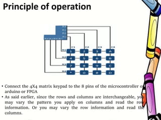
  • 9. • Connect the 4X4 matrix keypad to the 8 pins of the microcontroller or arduino or FPGA • As said earlier, since the rows and columns are interchangeable, you may vary the pattern you apply on columns and read the row information. Or you may vary the row information and read the columns. Principle of operation
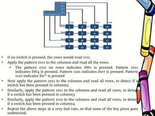
  • 10. • If no switch is pressed, the rows would read 1111. • Apply the pattern 0111 to the columns and read all the rows. • The pattern 0111 on rows indicates SW1 is pressed. Pattern 1011 indicates SW4 is pressed. Pattern 1101 indicates Sw7 is pressed. Pattern 1110 indicates Sw* is pressed • Next apply the pattern 1011 to the columns and read all rows, to detect if a switch has been pressed in column2. • Similarly, apply the pattern 1101 to the columns and read all rows, to detect if a switch has been pressed in column3 • Similarly, apply the pattern 1110 to the columns and read all rows, to detect if a switch has been pressed in column4 • Repeat the above steps at a very fast rate, so that none of the key press goes undetected.
  • 11. Summarizing, • It is the function of the microcontroller to scan the keyboard continuously to detect and identify the key pressed • To detect a pressed key, the microcontroller grounds all columns, successively, by providing 0 and then it reads the rows • If the data read from rows is 1111, no key has been pressed and the process continues till key press is detected • If one of the row bits has a zero, this means that a key press has occurred • After detecting a key press, microcontroller will go through the process of identifying the key Principle of operation
  • 12. Summarizing, • Starting with the Column 1, the microcontroller grounds it by providing a low to Column C0 only  It reads all the rows.  If the data read is all 1s, no key in that row is activated and the process is moved to the next column • It grounds the next column, reads all the rows and checks for any zero • This process continues until the column in which key is pressed is identified  After identification of the column in which the key has been pressed, Find out which row the pressed key belongs to Principle of operation
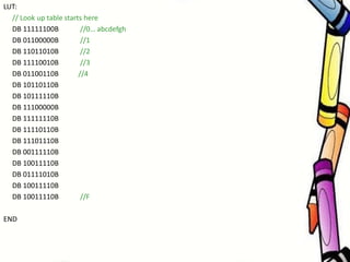
  • 13. ORG 00H MOV DPTR, #LUT // The 7-segment codes of switch press detected are stored in Code memory MOV P0, #00000000B // initializes P0 as output port; 7-segment is connected to Port 0 ;------------CONNECTIONS------------------ ;P1.0 = Col 0, P1.1 = Col 1, P1.2 = Col 2, P1.3 = Col 3, ;P1.4 = Row 0, P1.5 =Row 1 P1.6 = Row 2, P1.7 = Row 3, BACK: CLR P1.0 // makes Column 0 low,; col 1, col2 and col3 = 1 JB P1.4,NEXT1 // checks whether Row 0 is low and jumps to NEXT1 if not low MOV A,#1D // Row0 =0 when Col 0 =0,indicates that SW1 has been pressed. Display 1 ACALL DISPLAY // calls DISPLAY subroutine NEXT1:JB P1.5,NEXT2 // checks whether Row 1 is low. Row 1 =0 indicates SW2 has been pressed. MOV A,#2D // Display 2 ACALL DISPLAY NEXT2:JB P1.6,NEXT3// Check whether Row2 is low MOV A,#3D //Display 3 ACALL DISPLAY NEXT3:JB P1.7,NEXT4//Check if Row 3 is low MOV A,#10 D //Display A ACALL DISPLAY ; This completed one set of Row checking With Col0 =0. Next make Col0 =1 and col1=0, Col2 =1 and col3=1, as earlier 1 4 7 D 2 5 8 E 3 6 9 F A B C 0 P1.0 P1.1 P1.2 P1.3 P1.4 P1.5 P1.6 P1.7 Each keypad would have same internal connections, But the numbers displayed on top might vary. This code will work only for the keypad display shown
  • 14. ; column information = 1011, read rows NEXT4:SETB P1.0 CLR P1.1 JB P1.4,NEXT5 MOV A,#4D ACALL DISPLAY NEXT5:JB P1.5,NEXT6 MOV A,#5D ACALL DISPLAY NEXT6:JB P1.6,NEXT7 MOV A,#6D ACALL DISPLAY NEXT7:JB P1.7,NEXT8 MOV A,#11D ACALL DISPLAY ; column information = 1101, read rows NEXT8:SETB P1.1 CLR P1.2 JB P1.4,NEXT9 MOV A,#7D ACALL DISPLAY NEXT9:JB P1.5,NEXT10 MOV A,#8D ACALL DISPLAY NEXT10:JB P1.6,NEXT11 MOV A,#9D ACALL DISPLAY NEXT11:JB P1.7,NEXT12 MOV A,#12D ACALL DISPLAY 1 4 7 D 2 5 8 E 3 6 9 F A B C 0 P1.0 P1.1 P1.2 P1.3 P1.4 P1.5 P1.6 P1.7
  • 15. ; column information = 1110, read rows NEXT12:SETB P1.2 CLR P1.3 JB P1.4,NEXT13 MOV A,#13D ACALL DISPLAY NEXT13:JB P1.5,NEXT14 MOV A,#14D ACALL DISPLAY NEXT14:JB P1.6,NEXT15 MOV A,#15D ACALL DISPLAY NEXT15:JB P1.7,BACK MOV A,#0D ACALL DISPLAY LJMP BACK ;DPTR points to first location of LUT. Accumulator contains the offset value to be added. Fetch the byte containing the Seven segment code from LUT (in Code memory) and display DISPLAY: MOVC A,@A+DPTR // MOV P0,A // puts corresponding digit drive pattern into P0 RET
  • 16. LUT: // Look up table starts here DB 11111100B //0… abcdefgh DB 01100000B //1 DB 11011010B //2 DB 11110010B //3 DB 01100110B //4 DB 10110110B DB 10111110B DB 11100000B DB 11111110B DB 11110110B DB 11101110B DB 00111110B DB 10011110B DB 01111010B DB 10011110B DB 10011110B //F END