SlideShare a Scribd company logo
LCD Interfacing
with 8051
.
Lecture Notes: 27th March 2018- 3rd April 2018
Sudhanshu Janwadkar
TA, ECED, SVNIT
Points to discuss
• Character LCD basics
• Pin description of Character LCD
• Understanding how to use character LCD
• Interfacing with 8051
Introduction
• LCD stands for Liquid Crystal Display
• Two types:
 Character LCD
 Graphics LCD
• Used to:
 Display information
• LCDs are being widely used, because they are:
 Easy to Interface
 Easy to procure
 Well documented
LCD is finding widespread use. Factors:
• The declining prices of LCD
• The ability to display numbers, characters, and
graphics
• Incorporation of a refreshing controller into the
LCD, thereby relieving the CPU of the task of
refreshing the LCD
• Ease of programming
Introduction
• A 16×2 Liquid Crystal Display can display 32
characters at a time in two rows
 16 characters in one row
• Each character in the display of size 5×7 pixel
matrix, (although this matrix differs for
different 16×2 LCD modules)
• There are 16 pins in the LCD module
Introduction
LCD Interacing with 8051
• 5 X7 pixel matrix would mean there are 5 pixels in a
row and 7 pixels in a column for display.
• Each pixel will either be black or white to represent a
character.
• The character ‘A’ would be represented as shown:
Introduction
LCD Interacing with 8051
Pin Description of LCD
• Holding LCD towards the user, Leftmost pin is
pin 1 and rightmost is pin 16
• We can divide the LCD pins into following
categories:
 Power (Pin 1,2 and 3)
 Control (Pin 4, 5 and 6)
 Data (Pin 7 through 14)
 Backlight (Pin 15 and 16)
Pin Description of LCD
Power pins
• Pin 1 is Ground. Connect it to 0v.
• Pin 2 is VDD.
 You can connect it to 5V or 3.3V (Refer to data sheet of the LCD)
• Pin 3 is contrast pin.
 A typical character LCD would have black text in foreground
and green/blue background.
 Contrast would control the difference between background and
foreground.
 This pin would be required to make the display more dark (text
dark)
 Connect Pin3 to centre point of potentiometer and adjust
contrast with help of potentiometer.
Pin Description of LCD
Control pins
• Pin 4 is RS (Register Select)
 The LCDs have two registers: Command register & data
register in a DDRAM memory.
 The control instructions like clear LCD or shift the cursor, are
stored in Command Register (also called instruction register)
 The data to be displayed such as say some character ‘a’ ‘2’ etc, it
is stored in Data register.
 If you need to send command, select the command register by
setting RS=0. If you need to send data to be displayed on LCD,
you would select data register by setting RS=1
Pin Description of LCD
Control pins
• Pin Number 5 is Read/Write pin.
 Typically, you do not read from LCD, you write to it. Hence,
most of times, you would connect it to ground.
 If you would have to read data previously stored it LCD, you
would have to make this pin 1
• Pin 6 is enable pin.
 The transitions of Enable pin are seen as clock for the registers
in LCD. Data is latched on LCD only on positive edges of the
clock (Enable pin).
 Whenever you need to write data or command to a LCD or read
from LCD, you would have to generate a high-to low pulse on
Enable pin . Seeing this transition on LCD, the LCD would
understand that it has to perform a read/write operation.
Pin Description of LCD
Data pins
• Pin Number 7 through 14 are data pins.
 You can use 4 data pins or 8 data pins, for programming your
LCD.
 If you decide to use LCD in 4-bit mode, although the
data/command that is to be send to the LCD is of 8-bits width,
you would first send lower 4 bits of data and later you would
send the upper 4-bits, i.e. lower nibble followed by the upper
one.
 Why would one go for 4-bit mode when he/she can send 8-bit
data, at a time?
 4-bit mode saves 4-pins of the microcontroller. If your
application involves multiple interfaces, it would be wiser to
save the pins of microcontroller.
 If the application has no constraints on number of pins, it would
be wiser to use 8-bit mode as LCD writing is a slow speed
operation. You do not send any high priority data to LCD. Hence,
to make your application work faster, prefer 8-bit mode in this
case.
Pin Description of LCD
Backlight pins
• Pins 15 and 16 are for controlling Backlight
 Backlight is a LED in background.
 To control the backlight, you would connect pin 15 to positive
voltage and pin 16 to negative voltage. This would light up the
LED.
 Always connect this via a resistor, as you do not want to
damage the LED.
Pin Description of LCD
Category Pin Pin Name Function
Power Pins
1 VSS Ground Pin, connected to Ground
2 VDD or Vcc Voltage Pin (+5V or 3.3 V)
Contrast Pin 3 V0 or VEE
Contrast Setting, connected to Vcc thorough a
variable resistor.
Control Pins
4 RS
Register Select Pin
RS=0 Command mode
RS=1 Data mode
5 RW
Read/ Write pin,
RW=0 Write mode,
RW=1 Read mode
6 E
Enable, a high to low pulse need to enable the
LCD
Data Pins 7-14 D0-D7
Data Pins, Stores the Data to be displayed on
LCD or the command instructions
Backlight Pins
15 LED+ or A To power the Backlight +5V
16 LED- or K Backlight Ground
Pin Description of LCD - Summary
• RS: RS is the register select pin. You need to set it to 1, if you are
sending some data to be displayed on LCD.
– And you will set it to 0 if you are sending some command
instruction like clear the screen (hex code 01).
• RW: This is Read/write pin, you will set it to 0, if you are going
to write some data on LCD.
– And set it to 1, if you are reading from LCD module.
– Generally this is set to 0, because you do not have need to
read data from LCD.
• E: This pin is used to enable the module when a high to low pulse
is given to it.
– That transition from HIGH to LOW makes the module
ENABLE.
The Three important Control pins
Pin Description of LCD
LCD Control Instructions
Hex
Code
Command to LCD Instruction Register
0F LCD ON, cursor ON
01 Clear display screen
02 Return home
04 Decrement cursor (shift cursor to left)
06 Increment cursor (shift cursor to right)
05 Shift display right
07 Shift display left
0E Display ON, cursor blinking
80 Force cursor to beginning of first line
C0 Force cursor to beginning of second line
38 2 lines and 5×7 matrix
83 Cursor line 1 position 3
3C Activate second line
08 Display OFF, cursor OFF
C1 Jump to second line, position 1
OC Display ON, cursor OFF
Note; This is not an exclusive list of LCD instructions. The user would have to refer to
datasheet of LCD he/she is using
• Commonly used LCD instructions
• Each command is a 8-bit hexadecimal data
LCD Control Instructions
Command Interpretation
30 H LCD interprets this as the user would like to set LCD in 8-bit
mode, use only 1 line (row) of LCD and the font size of 5X7 (i.e.
5 dots (pixels) in row and 7 dots (pixels) in a column)
38 H Same as above, two lines would be used
20 H LCD interprets this as the user would like to set LCD in 4-bit
mode, use only 1 line (row) of LCD and the font size of 5X7 (i.e.
5 dots (pixels) in row and 7 dots (pixels) in a column)
28 H same as above, two lines would be used.
0E H Display is on, cursor is also on and is blinking
06 H Shift the cursor right
01 H Clear the display (i.e. the contents of LCD registers will be
erased)
80H-8FH Cursor positions in first row
C0H-CFH Cursor positions in second row
Steps to write Command/Data to LCD
Steps for displaying a character or data
• RS=1; Register select should be high
• R/W=0; Read/Write pin should be low.
• E=1->0; enable pin should be given high to
low pulse
Steps to send a command to the LCD
• RS=0; Register select should be low
• R/W=1; Read/Write pin should be high
• E=1->0; enable pin should be given high to
low pulse
Interfacing 16 X 2 LCD with 8051
Writing a code• ;------------- PIN CONNECTIONS------------------------------
//Port equ P0 ;data port to connect LCD
RS equ P2.2 ;RS pin connection
RW equ P2.3 ;RW pin connection
EN equ P2.4 ;EN pin connection
; P0 is connected to data pins of LCD
ACALL init ; Subroutine for initialising the LCD
;------------------------------------------------------------
MOV A, #‘H' ; Display ‘Hi‘ in first line of LCD
ACALL lcd_data
MOV A, #’i'
ACALL lcd_data
;------------------------------------------------------------
MOV A, #0c0H ;switch to 2nd line of LCD
ACALL lcd_cmd
MOV A, #‘P' ; Display ‘Pie'
ACALL lcd_data
MOV A, #‘i'
ACALL lcd_data
MOV A, #‘e'
ACALL lcd_data
HERE: SJMP HERE ; Infinite loop to keep displaying Hi, Pie
;--------LCD INITIALISATION------------------
init:
MOV A, #38H ; 16X 2 display, use both rows, 8bit mode; 5X7 pixel matrix
ACALL lcd_cmd
MOV A, #0EH ; display on cursor blinking
ACALL lcd_cmd
MOV A, #01H ; clear the display
ACALL lcd_cmd
RET
;------------------DELAY SUBROUTINE-------------------
delay:
MOV R0, #10H
L2: MOV R1,#0FH
L1: DJNZ R1, L1
DJNZ R0, L2
RET
lcd_cmd:
CLR RS ;clear rs, going to send command
CLR RW ;clear rw, write LCD operation
MOV P0,A ;put content of A to port
SETB EN ;make EN high
ACALL DELAY ;call a short delay routine
CLR EN ;clear EN
ACALL DELAY ; short delay
RET ;return
lcd_data:
SETB RS ;clear rs, going to send command
CLR RW ;clear rw, write LCD operation
MOV P0,A ;put content of A to port
SETB EN ;make EN high
ACALL DELAY ;call a short delay routine
CLR EN ;clear EN
ACALL DELAY ; short delay
RET ;return
END
1. The LCD register accepts the ASCII value. Send the
ASCII value of data to be displayed.
2. If required, include a Binary to ASCII subroutine
3. If 4bit mode is to be used, use masking subroutine
and split data

More Related Content

What's hot (20)

PPTX
Serial Communication in 8051
Sudhanshu Janwadkar
 
PPT
Adc interfacing
Monica Gunjal
 
PPTX
PLDs
VisualBee.com
 
PPTX
8086 in minimum mode
Sridari Iyer
 
PPTX
8051 MICROCONTROLLER ARCHITECTURE.pptx
MemonaMemon1
 
PPT
8051 instruction set
Andri Prastiyo
 
PPTX
4.programmable dma controller 8257
MdFazleRabbi18
 
PPTX
8051 Microcontroller ppt
Rahul Kumar
 
PDF
8086 modes
PDFSHARE
 
PPT
Microcontroller-8051.ppt
Dr.YNM
 
PPTX
8051 Microcontroller PPT's By Er. Swapnil Kaware
Prof. Swapnil V. Kaware
 
PPTX
Interfacing Stepper motor with 8051
Pantech ProLabs India Pvt Ltd
 
PPT
Memory organization of 8051
Muthu Manickam
 
PPTX
DRAM
rohitladdu
 
PPT
Memory & I/O interfacing
deval patel
 
PPTX
8255 PPI
deval patel
 
PPTX
MICROCONTROLLER 8051- Architecture & Pin Configuration
AKHIL MADANKAR
 
PDF
8259 Programmable Interrupt Controller
abhikalmegh
 
PPT
pin-diagram-details-of-8086-microprocessor
barsharoy19
 
PPTX
Instruction Set of 8051 Microcontroller
Multisoft Virtual Academy
 
Serial Communication in 8051
Sudhanshu Janwadkar
 
Adc interfacing
Monica Gunjal
 
8086 in minimum mode
Sridari Iyer
 
8051 MICROCONTROLLER ARCHITECTURE.pptx
MemonaMemon1
 
8051 instruction set
Andri Prastiyo
 
4.programmable dma controller 8257
MdFazleRabbi18
 
8051 Microcontroller ppt
Rahul Kumar
 
8086 modes
PDFSHARE
 
Microcontroller-8051.ppt
Dr.YNM
 
8051 Microcontroller PPT's By Er. Swapnil Kaware
Prof. Swapnil V. Kaware
 
Interfacing Stepper motor with 8051
Pantech ProLabs India Pvt Ltd
 
Memory organization of 8051
Muthu Manickam
 
Memory & I/O interfacing
deval patel
 
8255 PPI
deval patel
 
MICROCONTROLLER 8051- Architecture & Pin Configuration
AKHIL MADANKAR
 
8259 Programmable Interrupt Controller
abhikalmegh
 
pin-diagram-details-of-8086-microprocessor
barsharoy19
 
Instruction Set of 8051 Microcontroller
Multisoft Virtual Academy
 

Similar to LCD Interacing with 8051 (20)

PPTX
LCD (2).pptx
AjayPrajapathi
 
PPT
Lcd interfacing1
Monica Gunjal
 
PPTX
Lcd interfacing with microprocessor 8051
Hasnain Yaseen
 
DOCX
Lcd interfacing
AshuKaranam
 
PPTX
131080111003 mci
jokersclown57
 
PPT
Lcd interface with atmega32 avr best.ppt
SoumyaGupta836456
 
DOCX
Alp lcd
Caleb Joshua
 
DOCX
Lcd display
Nelarapu Mahesh
 
PDF
Lcd tutorial
Sujan Heuju
 
PDF
08_lcd.pdf
ssusera55490
 
PPTX
LCD_Example.pptx
julioalexanderaguila
 
PPTX
LCD interfacing
Kshitij Wagle
 
PDF
Embedded C Programming Module 7 Presentation
MarkkandanS
 
PPTX
8051_interface_LCD.pptx iii ece III ECE MPMC jntu k syllabus this is very he...
Kishore5511
 
PDF
Experiment 16 x2 parallel lcd
Prashanta Chowdhury
 
PDF
Microcontroller part 4
Keroles karam khalil
 
PPTX
Micro c lab6(lcd)
Mashood
 
PDF
AVR_Course_Day5 avr interfaces
Mohamed Ali
 
PDF
_LCD display-mbed.pdf
vidhyalakshmi153619
 
PPTX
Lcd interfaing using 8051 and assambly language programming
Vikas Dongre
 
LCD (2).pptx
AjayPrajapathi
 
Lcd interfacing1
Monica Gunjal
 
Lcd interfacing with microprocessor 8051
Hasnain Yaseen
 
Lcd interfacing
AshuKaranam
 
131080111003 mci
jokersclown57
 
Lcd interface with atmega32 avr best.ppt
SoumyaGupta836456
 
Alp lcd
Caleb Joshua
 
Lcd display
Nelarapu Mahesh
 
Lcd tutorial
Sujan Heuju
 
08_lcd.pdf
ssusera55490
 
LCD_Example.pptx
julioalexanderaguila
 
LCD interfacing
Kshitij Wagle
 
Embedded C Programming Module 7 Presentation
MarkkandanS
 
8051_interface_LCD.pptx iii ece III ECE MPMC jntu k syllabus this is very he...
Kishore5511
 
Experiment 16 x2 parallel lcd
Prashanta Chowdhury
 
Microcontroller part 4
Keroles karam khalil
 
Micro c lab6(lcd)
Mashood
 
AVR_Course_Day5 avr interfaces
Mohamed Ali
 
_LCD display-mbed.pdf
vidhyalakshmi153619
 
Lcd interfaing using 8051 and assambly language programming
Vikas Dongre
 
Ad

More from Sudhanshu Janwadkar (20)

PPTX
Presentation on Elementary Data Link Protocols
Sudhanshu Janwadkar
 
PPTX
Error Correcting and Error Detecting Codes.pptx
Sudhanshu Janwadkar
 
PPTX
DSP Processors versus ASICs
Sudhanshu Janwadkar
 
PPT
ASIC design Flow (Digital Design)
Sudhanshu Janwadkar
 
PPTX
Fpga architectures and applications
Sudhanshu Janwadkar
 
PPTX
Interrupts in 8051
Sudhanshu Janwadkar
 
PPT
SPI Bus Protocol
Sudhanshu Janwadkar
 
PPTX
I2C Protocol
Sudhanshu Janwadkar
 
PPTX
Introduction to 8051 Timer/Counter
Sudhanshu Janwadkar
 
PPTX
Intel 8051 Programming in C
Sudhanshu Janwadkar
 
PPTX
Hardware View of Intel 8051
Sudhanshu Janwadkar
 
PPTX
Architecture of the Intel 8051 Microcontroller
Sudhanshu Janwadkar
 
PPTX
Introduction to Embedded Systems
Sudhanshu Janwadkar
 
PPTX
CMOS Logic
Sudhanshu Janwadkar
 
PPTX
Interconnects in Reconfigurable Architectures
Sudhanshu Janwadkar
 
PPTX
Introduction to FPGAs
Sudhanshu Janwadkar
 
PDF
Design and Implementation of a GPS based Personal Tracking System
Sudhanshu Janwadkar
 
PDF
Embedded Logic Flip-Flops: A Conceptual Review
Sudhanshu Janwadkar
 
PPTX
Pass Transistor Logic
Sudhanshu Janwadkar
 
PPTX
Memory and Processor Testing
Sudhanshu Janwadkar
 
Presentation on Elementary Data Link Protocols
Sudhanshu Janwadkar
 
Error Correcting and Error Detecting Codes.pptx
Sudhanshu Janwadkar
 
DSP Processors versus ASICs
Sudhanshu Janwadkar
 
ASIC design Flow (Digital Design)
Sudhanshu Janwadkar
 
Fpga architectures and applications
Sudhanshu Janwadkar
 
Interrupts in 8051
Sudhanshu Janwadkar
 
SPI Bus Protocol
Sudhanshu Janwadkar
 
I2C Protocol
Sudhanshu Janwadkar
 
Introduction to 8051 Timer/Counter
Sudhanshu Janwadkar
 
Intel 8051 Programming in C
Sudhanshu Janwadkar
 
Hardware View of Intel 8051
Sudhanshu Janwadkar
 
Architecture of the Intel 8051 Microcontroller
Sudhanshu Janwadkar
 
Introduction to Embedded Systems
Sudhanshu Janwadkar
 
Interconnects in Reconfigurable Architectures
Sudhanshu Janwadkar
 
Introduction to FPGAs
Sudhanshu Janwadkar
 
Design and Implementation of a GPS based Personal Tracking System
Sudhanshu Janwadkar
 
Embedded Logic Flip-Flops: A Conceptual Review
Sudhanshu Janwadkar
 
Pass Transistor Logic
Sudhanshu Janwadkar
 
Memory and Processor Testing
Sudhanshu Janwadkar
 
Ad

Recently uploaded (20)

DOCX
Unit 5: Speech-language and swallowing disorders
JELLA VISHNU DURGA PRASAD
 
PPTX
Digital Professionalism and Interpersonal Competence
rutvikgediya1
 
PPTX
INTESTINALPARASITES OR WORM INFESTATIONS.pptx
PRADEEP ABOTHU
 
PPTX
Continental Accounting in Odoo 18 - Odoo Slides
Celine George
 
PDF
Antianginal agents, Definition, Classification, MOA.pdf
Prerana Jadhav
 
PPTX
Translation_ Definition, Scope & Historical Development.pptx
DhatriParmar
 
PPTX
Dakar Framework Education For All- 2000(Act)
santoshmohalik1
 
PPTX
I INCLUDED THIS TOPIC IS INTELLIGENCE DEFINITION, MEANING, INDIVIDUAL DIFFERE...
parmarjuli1412
 
PPTX
YSPH VMOC Special Report - Measles Outbreak Southwest US 7-20-2025.pptx
Yale School of Public Health - The Virtual Medical Operations Center (VMOC)
 
PPTX
Cleaning Validation Ppt Pharmaceutical validation
Ms. Ashatai Patil
 
PPTX
Introduction to Probability(basic) .pptx
purohitanuj034
 
PDF
Virat Kohli- the Pride of Indian cricket
kushpar147
 
PPTX
Rules and Regulations of Madhya Pradesh Library Part-I
SantoshKumarKori2
 
PPTX
The Future of Artificial Intelligence Opportunities and Risks Ahead
vaghelajayendra784
 
PPTX
TOP 10 AI TOOLS YOU MUST LEARN TO SURVIVE IN 2025 AND ABOVE
digilearnings.com
 
PDF
The Minister of Tourism, Culture and Creative Arts, Abla Dzifa Gomashie has e...
nservice241
 
DOCX
Modul Ajar Deep Learning Bahasa Inggris Kelas 11 Terbaru 2025
wahyurestu63
 
PPTX
ENGLISH 8 WEEK 3 Q1 - Analyzing the linguistic, historical, andor biographica...
OliverOllet
 
PPTX
K-Circle-Weekly-Quiz12121212-May2025.pptx
Pankaj Rodey
 
PPTX
Electrophysiology_of_Heart. Electrophysiology studies in Cardiovascular syste...
Rajshri Ghogare
 
Unit 5: Speech-language and swallowing disorders
JELLA VISHNU DURGA PRASAD
 
Digital Professionalism and Interpersonal Competence
rutvikgediya1
 
INTESTINALPARASITES OR WORM INFESTATIONS.pptx
PRADEEP ABOTHU
 
Continental Accounting in Odoo 18 - Odoo Slides
Celine George
 
Antianginal agents, Definition, Classification, MOA.pdf
Prerana Jadhav
 
Translation_ Definition, Scope & Historical Development.pptx
DhatriParmar
 
Dakar Framework Education For All- 2000(Act)
santoshmohalik1
 
I INCLUDED THIS TOPIC IS INTELLIGENCE DEFINITION, MEANING, INDIVIDUAL DIFFERE...
parmarjuli1412
 
YSPH VMOC Special Report - Measles Outbreak Southwest US 7-20-2025.pptx
Yale School of Public Health - The Virtual Medical Operations Center (VMOC)
 
Cleaning Validation Ppt Pharmaceutical validation
Ms. Ashatai Patil
 
Introduction to Probability(basic) .pptx
purohitanuj034
 
Virat Kohli- the Pride of Indian cricket
kushpar147
 
Rules and Regulations of Madhya Pradesh Library Part-I
SantoshKumarKori2
 
The Future of Artificial Intelligence Opportunities and Risks Ahead
vaghelajayendra784
 
TOP 10 AI TOOLS YOU MUST LEARN TO SURVIVE IN 2025 AND ABOVE
digilearnings.com
 
The Minister of Tourism, Culture and Creative Arts, Abla Dzifa Gomashie has e...
nservice241
 
Modul Ajar Deep Learning Bahasa Inggris Kelas 11 Terbaru 2025
wahyurestu63
 
ENGLISH 8 WEEK 3 Q1 - Analyzing the linguistic, historical, andor biographica...
OliverOllet
 
K-Circle-Weekly-Quiz12121212-May2025.pptx
Pankaj Rodey
 
Electrophysiology_of_Heart. Electrophysiology studies in Cardiovascular syste...
Rajshri Ghogare
 

LCD Interacing with 8051

  • 1. LCD Interfacing with 8051 . Lecture Notes: 27th March 2018- 3rd April 2018 Sudhanshu Janwadkar TA, ECED, SVNIT
  • 2. Points to discuss • Character LCD basics • Pin description of Character LCD • Understanding how to use character LCD • Interfacing with 8051
  • 3. Introduction • LCD stands for Liquid Crystal Display • Two types:  Character LCD  Graphics LCD • Used to:  Display information • LCDs are being widely used, because they are:  Easy to Interface  Easy to procure  Well documented
  • 4. LCD is finding widespread use. Factors: • The declining prices of LCD • The ability to display numbers, characters, and graphics • Incorporation of a refreshing controller into the LCD, thereby relieving the CPU of the task of refreshing the LCD • Ease of programming Introduction
  • 5. • A 16×2 Liquid Crystal Display can display 32 characters at a time in two rows  16 characters in one row • Each character in the display of size 5×7 pixel matrix, (although this matrix differs for different 16×2 LCD modules) • There are 16 pins in the LCD module Introduction
  • 7. • 5 X7 pixel matrix would mean there are 5 pixels in a row and 7 pixels in a column for display. • Each pixel will either be black or white to represent a character. • The character ‘A’ would be represented as shown: Introduction
  • 10. • Holding LCD towards the user, Leftmost pin is pin 1 and rightmost is pin 16 • We can divide the LCD pins into following categories:  Power (Pin 1,2 and 3)  Control (Pin 4, 5 and 6)  Data (Pin 7 through 14)  Backlight (Pin 15 and 16) Pin Description of LCD
  • 11. Power pins • Pin 1 is Ground. Connect it to 0v. • Pin 2 is VDD.  You can connect it to 5V or 3.3V (Refer to data sheet of the LCD) • Pin 3 is contrast pin.  A typical character LCD would have black text in foreground and green/blue background.  Contrast would control the difference between background and foreground.  This pin would be required to make the display more dark (text dark)  Connect Pin3 to centre point of potentiometer and adjust contrast with help of potentiometer. Pin Description of LCD
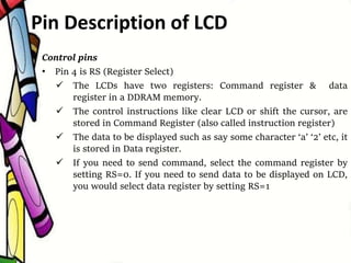
  • 12. Control pins • Pin 4 is RS (Register Select)  The LCDs have two registers: Command register & data register in a DDRAM memory.  The control instructions like clear LCD or shift the cursor, are stored in Command Register (also called instruction register)  The data to be displayed such as say some character ‘a’ ‘2’ etc, it is stored in Data register.  If you need to send command, select the command register by setting RS=0. If you need to send data to be displayed on LCD, you would select data register by setting RS=1 Pin Description of LCD
  • 13. Control pins • Pin Number 5 is Read/Write pin.  Typically, you do not read from LCD, you write to it. Hence, most of times, you would connect it to ground.  If you would have to read data previously stored it LCD, you would have to make this pin 1 • Pin 6 is enable pin.  The transitions of Enable pin are seen as clock for the registers in LCD. Data is latched on LCD only on positive edges of the clock (Enable pin).  Whenever you need to write data or command to a LCD or read from LCD, you would have to generate a high-to low pulse on Enable pin . Seeing this transition on LCD, the LCD would understand that it has to perform a read/write operation. Pin Description of LCD
  • 14. Data pins • Pin Number 7 through 14 are data pins.  You can use 4 data pins or 8 data pins, for programming your LCD.  If you decide to use LCD in 4-bit mode, although the data/command that is to be send to the LCD is of 8-bits width, you would first send lower 4 bits of data and later you would send the upper 4-bits, i.e. lower nibble followed by the upper one.  Why would one go for 4-bit mode when he/she can send 8-bit data, at a time?  4-bit mode saves 4-pins of the microcontroller. If your application involves multiple interfaces, it would be wiser to save the pins of microcontroller.  If the application has no constraints on number of pins, it would be wiser to use 8-bit mode as LCD writing is a slow speed operation. You do not send any high priority data to LCD. Hence, to make your application work faster, prefer 8-bit mode in this case. Pin Description of LCD
  • 15. Backlight pins • Pins 15 and 16 are for controlling Backlight  Backlight is a LED in background.  To control the backlight, you would connect pin 15 to positive voltage and pin 16 to negative voltage. This would light up the LED.  Always connect this via a resistor, as you do not want to damage the LED. Pin Description of LCD
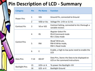
  • 16. Category Pin Pin Name Function Power Pins 1 VSS Ground Pin, connected to Ground 2 VDD or Vcc Voltage Pin (+5V or 3.3 V) Contrast Pin 3 V0 or VEE Contrast Setting, connected to Vcc thorough a variable resistor. Control Pins 4 RS Register Select Pin RS=0 Command mode RS=1 Data mode 5 RW Read/ Write pin, RW=0 Write mode, RW=1 Read mode 6 E Enable, a high to low pulse need to enable the LCD Data Pins 7-14 D0-D7 Data Pins, Stores the Data to be displayed on LCD or the command instructions Backlight Pins 15 LED+ or A To power the Backlight +5V 16 LED- or K Backlight Ground Pin Description of LCD - Summary
  • 17. • RS: RS is the register select pin. You need to set it to 1, if you are sending some data to be displayed on LCD. – And you will set it to 0 if you are sending some command instruction like clear the screen (hex code 01). • RW: This is Read/write pin, you will set it to 0, if you are going to write some data on LCD. – And set it to 1, if you are reading from LCD module. – Generally this is set to 0, because you do not have need to read data from LCD. • E: This pin is used to enable the module when a high to low pulse is given to it. – That transition from HIGH to LOW makes the module ENABLE. The Three important Control pins Pin Description of LCD
  • 18. LCD Control Instructions Hex Code Command to LCD Instruction Register 0F LCD ON, cursor ON 01 Clear display screen 02 Return home 04 Decrement cursor (shift cursor to left) 06 Increment cursor (shift cursor to right) 05 Shift display right 07 Shift display left 0E Display ON, cursor blinking 80 Force cursor to beginning of first line C0 Force cursor to beginning of second line 38 2 lines and 5×7 matrix 83 Cursor line 1 position 3 3C Activate second line 08 Display OFF, cursor OFF C1 Jump to second line, position 1 OC Display ON, cursor OFF Note; This is not an exclusive list of LCD instructions. The user would have to refer to datasheet of LCD he/she is using
  • 19. • Commonly used LCD instructions • Each command is a 8-bit hexadecimal data LCD Control Instructions Command Interpretation 30 H LCD interprets this as the user would like to set LCD in 8-bit mode, use only 1 line (row) of LCD and the font size of 5X7 (i.e. 5 dots (pixels) in row and 7 dots (pixels) in a column) 38 H Same as above, two lines would be used 20 H LCD interprets this as the user would like to set LCD in 4-bit mode, use only 1 line (row) of LCD and the font size of 5X7 (i.e. 5 dots (pixels) in row and 7 dots (pixels) in a column) 28 H same as above, two lines would be used. 0E H Display is on, cursor is also on and is blinking 06 H Shift the cursor right 01 H Clear the display (i.e. the contents of LCD registers will be erased) 80H-8FH Cursor positions in first row C0H-CFH Cursor positions in second row
  • 20. Steps to write Command/Data to LCD Steps for displaying a character or data • RS=1; Register select should be high • R/W=0; Read/Write pin should be low. • E=1->0; enable pin should be given high to low pulse Steps to send a command to the LCD • RS=0; Register select should be low • R/W=1; Read/Write pin should be high • E=1->0; enable pin should be given high to low pulse
  • 21. Interfacing 16 X 2 LCD with 8051
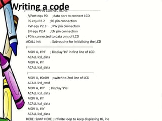
  • 22. Writing a code• ;------------- PIN CONNECTIONS------------------------------ //Port equ P0 ;data port to connect LCD RS equ P2.2 ;RS pin connection RW equ P2.3 ;RW pin connection EN equ P2.4 ;EN pin connection ; P0 is connected to data pins of LCD ACALL init ; Subroutine for initialising the LCD ;------------------------------------------------------------ MOV A, #‘H' ; Display ‘Hi‘ in first line of LCD ACALL lcd_data MOV A, #’i' ACALL lcd_data ;------------------------------------------------------------ MOV A, #0c0H ;switch to 2nd line of LCD ACALL lcd_cmd MOV A, #‘P' ; Display ‘Pie' ACALL lcd_data MOV A, #‘i' ACALL lcd_data MOV A, #‘e' ACALL lcd_data HERE: SJMP HERE ; Infinite loop to keep displaying Hi, Pie
  • 23. ;--------LCD INITIALISATION------------------ init: MOV A, #38H ; 16X 2 display, use both rows, 8bit mode; 5X7 pixel matrix ACALL lcd_cmd MOV A, #0EH ; display on cursor blinking ACALL lcd_cmd MOV A, #01H ; clear the display ACALL lcd_cmd RET ;------------------DELAY SUBROUTINE------------------- delay: MOV R0, #10H L2: MOV R1,#0FH L1: DJNZ R1, L1 DJNZ R0, L2 RET
  • 24. lcd_cmd: CLR RS ;clear rs, going to send command CLR RW ;clear rw, write LCD operation MOV P0,A ;put content of A to port SETB EN ;make EN high ACALL DELAY ;call a short delay routine CLR EN ;clear EN ACALL DELAY ; short delay RET ;return lcd_data: SETB RS ;clear rs, going to send command CLR RW ;clear rw, write LCD operation MOV P0,A ;put content of A to port SETB EN ;make EN high ACALL DELAY ;call a short delay routine CLR EN ;clear EN ACALL DELAY ; short delay RET ;return END
  • 25. 1. The LCD register accepts the ASCII value. Send the ASCII value of data to be displayed. 2. If required, include a Binary to ASCII subroutine 3. If 4bit mode is to be used, use masking subroutine and split data