Lecture1 The 8085 Microprocessor
0 likes102 views

The document details the architecture of the 8085 microprocessor, including its registers, arithmetic logic unit, and control units. It highlights the 8085's features, such as it being an 8-bit microprocessor with a clock speed of approximately 3 MHz, a memory addressing capability of 64 kB, and various input/output control functions. Additionally, the document explains the operation of interrupts and direct memory access (DMA) to enhance data transfer efficiency.


Lecture1 The 8085 Microprocessor
- 1. Presented by: Engr Zeeshan Ahmed Lodro Lecturer-Department of Electronics Engineering Technology BBS University of Technology and Skill Development Khairpur Mirs 1 Lecture-01
- 2. 2
- 3. ❑InternalArchitecture of 8085 Microprocessor ▪ Register Section ▪ Arithmetic Logic Unit ▪ Timing and Control Unit ▪ Interrupt Control ▪ IO Control ❑ Pin Description of 8085 3
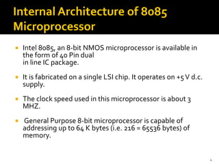
- 4. Intel 8085, an 8-bit NMOS microprocessor is available in the form of 40 Pin dual in line IC package. It is fabricated on a single LSI chip. It operates on +5V d.c. supply. The clock speed used in this microprocessor is about 3 MHZ. General Purpose 8-bit microprocessor is capable of addressing up to 64 K bytes (i.e. 216 = 65536 bytes) of memory. 4
- 5. (I) Register Section (ii) Arithmetic and Logic Unit (iii)Timing and Control Section (iv) Interrupt Control (v) Serial Input / Output Control 5
- 6. 6
- 7. The 8085 microprocessor contains eight addressable 8-bit registers namely: 1. A (Accumulator) register 2. F Flag register (Flag flip-flops) 3. B register 4. C register 5. D register 6. E register 7. H register 8. L register 7
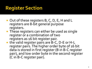
- 8. Out of these registers B, C, D, E, H and L registers are 8-bit general purpose registers. These registers can either be used as single register or a combination of two registers as 16 bit register pair. the valid register pairs are B-C, D-E or H-L register pairs.The higher order byte of 16 bit data is stored in first register (B in B-C register pair), and low order byte in the second register (C in B-C register pair). 8
- 9. The H-L register pair can also be used for register indirect addressing; since this register pair can also function as data pointer. The large number of general purpose registers gives more flexibility and ease in the programming. However, the general purpose registers are limited as registers occupy more space on the silicon chip. Beside these general purpose registers, the 8085 has remaining two 8-bit registers Accumulator (A) and Flag (F) as special purpose registers and two 16 bit registers namely Program counter (PC) and stack pointer (SP) 9
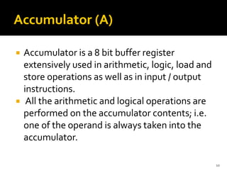
- 10. Accumulator is a 8 bit buffer register extensively used in arithmetic, logic, load and store operations as well as in input / output instructions. All the arithmetic and logical operations are performed on the accumulator contents; i.e. one of the operand is always taken into the accumulator. 10
- 11. It is an 8-bit register associated with the execution of instructions in the microprocessor. Out of the 8 bits of flag register, 5 bits contains significant information in terms of status flags. The five flags are: (i) Sign flag (S) (ii) Zero flag (Z) (iii) Carry flag (CY) (iv) Parity flag (P) (v) Auxiliary Carry flag (AC) 11
- 12. The bit positions reserved for these flags in the flag register (F) 12
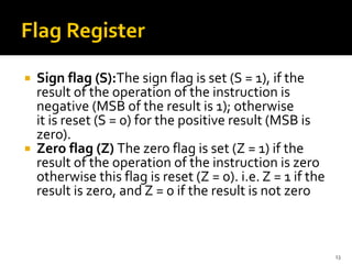
- 13. Sign flag (S):The sign flag is set (S = 1), if the result of the operation of the instruction is negative (MSB of the result is 1); otherwise it is reset (S = 0) for the positive result (MSB is zero). Zero flag (Z) The zero flag is set (Z = 1) if the result of the operation of the instruction is zero otherwise this flag is reset (Z = 0). i.e. Z = 1 if the result is zero, and Z = 0 if the result is not zero 13
- 14. Carry flag (CY) The carry flag is set to 1, if there exist a carry (or borrow) to the highest order bit (non-existent 9th position) as a result of the execution of addition or subtraction instructions. If there is no carry (or borrow) to the higher order bit, the carry flag is reset. i.e. CY = 1 if there is a carry to the highest order bit (or overflow), and CY = 0 if there is no carry to the highest order bit (or no overflow) 14
- 15. Parity flag (P) After an arithmetic and logic operation, if the result has even number of 1s, then parity bit is set. If on the other hand the result has odd number of 1s, the parity flag is reset. i.e. P = 1, if the result has even number of 1s, and P = 0, if the result has odd number of 1s. 15
- 16. Auxiliary carry (AC) This is a new flag in 8085 microprocessor.This flag (AC) is set to 1, if there is an overflow at bit 3 of the accumulator. AC flag is used in BCD arithmetic.This is illustrated as given below: 16
- 17. The program counter is a 16 bit register. It is used to send 16 bit address to fetch the instruction from the memory. It acts as a pointer which indicates the address of the next instruction to be fetched and executed. The program counter is updated after an instruction has been fetched by the processor. If an instruction is one byte instruction , then the program counter will be updated by one (i.e. PC = PC + 1). Similarly, for two and three byte instructions, the program counter will be updated by two (i.e. PC=PC+2) or three (i.e. PC=PC + 3) locations respectively. 17
- 18. The stack is an area of RAM (random access memory or read / write memory) in which temporary information is stored. It is stored on First-In-Last-Out (FILO) basis. An address in the RAM area is assigned to the stack pointer where the first information is stored as the first stack entry. This is done by initializing stack pointer by an instruction. Higher stack entries are made at the progressively decreasing addresses. 18
- 19. 8085 requires 8-bit data bus and 16-bit address bus, as the memory address is of 16 bits. More number of IC pins are required if separate address and data bus are introduced. To restrict the number of pins of 8085 to only 40, lower address linesA0- A7 and data lines D0-D7 are used in multiplexed mode. The multiplexed lines are designed as Address/Data Bus (AD0-AD7). So whenever 16-bit address is transmitted by the microprocessor 8 MSBs of the address lines are sent on the Address Bus (A15-A8) and 8 LSBs of the lines are sent on the Address/Data Bus (AD7-AD0). The 8 LSBs of the address are then latched either into memory or external latch so that the complete address remains available for further operation. The 8-bit Address/Data Bus will now be free for the data transmission 19
- 20. The arithmetic and logical unit (ALU) basically consists of accumulator (A), flag register (F) and a temporary register (which is inaccessible by the programmer or user). This unit carries out the arithmetic and logic calculations of the data stored in general purpose registers or in memory locations. The arithmetic operations are ADD, SUB, compare, increments, decrements and complements etc.; while logical operations are AND, OR, XOR and Rotate.The result of these operations could be placed in the accumulator or elsewhere through the internal bus. Arithmetic operations are usually carried out in 2’s complement adder / subtrator discussed in the preceding chapter. For these operations,ALU receives the control signals from the timing and control unit. 20
- 21. Timing and Control Unit This unit consists of the following sections: 1. Instruction Register and Decoder 2. Control signals 21
- 22. The CPU fetches an instruction from the memory for its execution.This instruction can be of 1-3 byte long. The first byte contains the op code of instruction which basically specifies the nature of operation to be performed indicating the length of the instruction. The first byte (op code of the instruction) transferred to 8-bit instruction register through the internal bus of the CPU , becomes available at the instruction decoder. The decoder decodes the op code and directs the control unit to produce the necessary control signals. 22
- 23. Following are the control signals of 8085 microprocessor needed for the operation of CPU. (i) X1, X2 and CLK Out Two pins X1 and X2 are provided to be externally connected to a quartz crystal. The clock signal of fixed frequency is generated through the internal circuitry of the processor. The frequency at which the microprocessor 8085 works is half of the crystal frequency. The quartz crystal of 6.144 MHz is used in this processor.This gives the clock frequency of 3.072 MHz (half of the crystal frequency) of 50% duty cycle. The clock period is of about 320 n sec. The output of the clock frequency is also available at CLK out terminal. 23
- 24. (ii) Address Latch Enable (ALE) The 16 bit address bus is basically divided into two sets. The most significant bits A7-A15 of the address bus are used separately and the least significant bits of the address AD0-AD7 are time multiplexed with the bits of bidirectional data bus (D0-D7). The AD0-AD7 bus serves the dual purpose as they can be used as low- order address bus as well as bidirectional data bus at different times. This is used as address bus, during the first clock cycle of the machine cycle involving memory; and during the remaining clock cycle of the machine cycle, it acts as the data bus. This is accomplished by address latch enable (ALE) signal provided in the processor. During the first clock cycle of the machine cycle ALE is high which enables the lower 8-bit of the address to be latched either into the memory or external latch. 24
- 25. (iii) Read Signal This is an active low signal to be connected to memory read input (output enable signal to memories) or to input / output read signal to enable input / output buffer (iv)WR (Write) Signal Similar to read signal ( RD ), write signal (WR ) is also active low.This signal is used to write to the memory or input / output devices (v) IO/ M (Input Output / Memory) This signal IO/ M distinguishes that the address and data is meant for either I/O devices or memory. Whenever this signal is high (1), microprocessor will communicate to the I/O devices and whenever it is low (0), microprocessor will communicate to the memory. 25
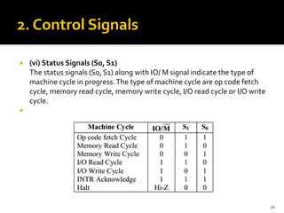
- 26. (vi) Status Signals (S0, S1) The status signals (S0, S1) along with IO/ M signal indicate the type of machine cycle in progress.The type of machine cycle are op code fetch cycle, memory read cycle, memory write cycle, I/O read cycle or I/O write cycle. 26
- 27. (vi) Hold and HLDA HOLD and HLDA (HoldAcknowledge) signals are used for DMA (Direct MemoryAccess) operation. In a microprocessor, the data transfer between I/O devices and memory will take place through the microprocessor. The involvement of the processor slows down the data transfer between I/O devices and memory. The transfer of data directly from I/O devices to memory without involvement of microprocessor is called DMA. 27
- 28. The DMA will save the time as CPU relinquishes the control of Buses. In this way DMA transfers the large amount of data in a relatively short time. The HOLD and HLDA signals are used in the operation. Whenever HOLD signal is high, CPU temporarily relinquishes its operation by floating the address, data and control buses; and DMA operation is started. A high HLDA (Hold Acknowledge) signal is also sent to DMA controller, indicating that CPU has received the hold request. Whenever the data transfer is complete, then the control to CPU is returned back by sending a HOLD signal. Further the HLDA signal goes low. 28
- 29. (viii) READY signal (Input) Some peripheral devices connected to 8085 microprocessor operate at much slower speed than the processor. To synchronize the speed of CPU and peripheral devices or to slow down the speed of 8085, the READY signal is used. If the READY signal is high the peripheral device is ready and the processor can complete the data transfer. If this signal is low the microprocessor waits (by generating a number of NOPT-states) till it goes high 29
- 30. (ix) and RESET OUT The signal may be low from the operator Reset button or from the processor. When the signal is low, the CPU will reset the program counter, instruction register and other circuits. It also sends a high RESET OUT. The RESET OUT signal goes to peripheral devices to reset or initialized. When signal goes high and RESET OUT goes low, the data processing may begin. 30
- 31. Sometimes it is necessary to interrupt the execution of the main program. For this an interrupt request is obtained from the I/O devices. After receiving the interrupt request (INTR), processor temporarily stops what it was doing and attends to the I/O device. INTA is an interrupt acknowledge signal which is sent by the microprocessor after INTR signal is received. After the work of the I/O device is complete it returns to what it was doing earlier. 31
- 32. Basically 8085A has five hardware interrupts namely: INTR RST 5.5 RST 6.5 RST 7.5 and TRAP If two or more of these interrupts are active at the same time, the 8085 takes them in order of priority level. 32
- 33. Serial input / output control circuit incorporated in this microprocessor is used for the data transmission. For this purpose two pins SID and SOD are provided in the serial input/output control unit. The SID (Serial Input Data) terminal receives the serial data stream from an input device, the control unit converts serial data stream to parallel data before it is used by the computer. After the conversion 8-bit parallel data is stored in the accumulator. Similarly, SOD (Serial Out Data) terminal outputs the 8-bit parallel available with the accumulator into serial form to the peripheral device connected with the computer 33
- 34. The pin details and logical schematics of the 40 pin dual line package (DIP) IC 8085 are shown 34
- 35. 35
- 36. 36
- 37. 37