Lecture14
Download as PPT, PDF1 like431 views

This document discusses power dissipation in VLSI systems. It defines power, energy, and average power. Dynamic power is required to charge and discharge load capacitances when transistors switch. Static power is consumed even when the chip is quiescent, due to leakage currents. Techniques for reducing power include lowering capacitance, supply voltage, frequency, and leakage through body biasing and temperature control. The document breaks down power sources and discusses dynamic voltage scaling to optimize power usage.


![Capacitive dynamic power
If the gate is switched on and off f0→1 (switching factor) times
per second, the power consumption is given by
For entire circuit
where αi is activity factor [0..0.5] in comparison to the clock
frequency (which has switching factor of 1)
Pdynamic = α CVDD 2 f
S. Reda EN160 SP’08](https://image.slidesharecdn.com/lecture14-120612013848-phpapp02/85/Lecture14-5-320.jpg)

![Dynamic power breakup
Gate
34%
Interconnect
51%
Diffusion
15%
Total dynamic Power
[source: Intel’03]
S. Reda EN160 SP’08](https://image.slidesharecdn.com/lecture14-120612013848-phpapp02/85/Lecture14-7-320.jpg)


Lecture14
- 1. Design and Implementation of VLSI Systems (EN1600) Lecture 14: Power Dissipation S. Reda EN160 SP’08
- 2. Power and Energy • Power is drawn from a voltage source attached to the VDD pin(s) of a chip. • Instantaneous Power: P(t ) = iDD (t )VDD T T • Energy: E = ∫ P(t )dt = ∫ iDD (t )VDD dt 0 0 T E 1 • Average Power: Pavg = = ∫ iDD (t )VDD dt T T 0 S. Reda EN160 SP’08
- 3. Dynamic power • Dynamic power is required to charge and discharge load capacitances when transistors switch. • One cycle involves a rising and falling output. • On rising output, charge Q = CVDD is required • On falling output, charge is dumped to GND VDD • This repeats Tfsw times iDD(t) over an interval of T C fsw S. Reda EN160 SP’08
- 4. Dynamic power dissipation Vdd Vin Vout load capacitance CL (gate + diffusion + interconnects) Energy delivered by the supply during input 1 → 0 transition: Energy stored at the capacitor at the end of 1 → 0 transition: dissipated in NMOS during discharge S. Reda EN160 SP’08 (input: 0 → 1)
- 5. Capacitive dynamic power If the gate is switched on and off f0→1 (switching factor) times per second, the power consumption is given by For entire circuit where αi is activity factor [0..0.5] in comparison to the clock frequency (which has switching factor of 1) Pdynamic = α CVDD 2 f S. Reda EN160 SP’08
- 6. Short circuit current • When transistors switch, both nMOS and pMOS networks may be momentarily ON at once • Leads to a blip of “short circuit” current. • < 10% of dynamic power if rise/fall times are comparable for input and output S. Reda EN160 SP’08
- 7. Dynamic power breakup Gate 34% Interconnect 51% Diffusion 15% Total dynamic Power [source: Intel’03] S. Reda EN160 SP’08
- 8. Static (leakage) power • Static power is consumed even when chip is quiescent. – Leakage draws power from nominally OFF devices Vgs −Vt −Vds I ds = I ds 0e nvT 1 − e vT S. Reda EN160 SP’08
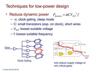
- 9. Techniques for low-power design • Reduce dynamic power Pdynamic = α CVDD 2 f – α: clock gating, sleep mode – C: small transistors (esp. on clock), short wires – VDD: lowest suitable voltage – f: lowest suitable frequency I1 I2 O1 Clock I3 I4 I5 O2 Enable I critical 6 path Clock Gating only reduce supply voltage of non critical gates S. Reda EN160 SP’08
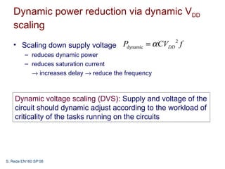
- 10. Dynamic power reduction via dynamic VDD scaling • Scaling down supply voltage Pdynamic = α CVDD f 2 – reduces dynamic power – reduces saturation current → increases delay → reduce the frequency Dynamic voltage scaling (DVS): Supply and voltage of the circuit should dynamic adjust according to the workload of criticality of the tasks running on the circuits S. Reda EN160 SP’08
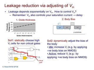
- 11. Leakage reduction via adjusting of Vth • Leakage depends exponentially on Vth. How to control Vth? – Remember: Vth also controls your saturation current → delay 1. Oxide thickness 2. Body Bias Sol1: statically choose high Sol2: dynamically adjust the bias of Vt cells for non critical gates the body I1 • idle: increase Vt (e.g. by applying I2 O1 –ve body bias on NMOS) I3 I4 • Active: reduce Vt (e.g.: by I5 O2 applying +ve body bias on NMOS) I critical 6 path S. Reda EN160 SP’08
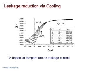
- 12. Leakage reduction via Cooling Impact of temperature on leakage current S. Reda EN160 SP’08
- 13. Summary We are still in chapter 4: Delay estimation Power estimation Interconnects and wire engineering Scaling theory S. Reda EN160 SP’08