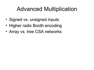
2. 2
Multiplexers
• A Multiplexer consists of n input lines and
one output line.
• 2:1 multiplexer chooses between two
inputs
S W1 W0 F
0 X 0 0
0 X 1 1
1 0 X 0
1 1 X 1
0
1
S
W0
W1
F
3. 3
Gate-Level Mux Design
•
• How many transistors are needed? 20
1 0 (too many transistors)
F SW SW
4
4
W1
W0
S F
4
2
2
2 F
2
W1
W0
S
4. 4
Transmission Gate Mux
• Non restoring MUX uses two transmission
gates
– Only 4 transistors S
S
W0
W1
F
S
5. • Verilog: 2x1 MUX
– Uses the conditional ?: operator
• Software designers detest this operator
• Hardware designers revel in its beauty
6. • Behavioral Style in Verilog
Must be reg type when used as LHS in
an always block
Sensitivity list: statements inside the always
block are only executed when one or more
signals in the list changes value
7. 7
4:1 Multiplexer
• 4:1 mux chooses one of 4 inputs using
two selects
– Two levels of 2:1 muxes
– Or four tristates
S0
D0
D1
0
1
0
1
0
1
Y
S1
D2
D3
D0
D1
D2
D3
Y
S1S0 S1S0 S1S0 S1S0
12. • Verilog: 4x1 MUX (Data Flow Style)
– This is getting complicated!
– Need a way to specify a “group” of bits like w[0:3]
– Need a way to replace ?: with “if then else”
13. • Vectored Signals in Verilog
Signals can be grouped as bit vectors
• The order of the bits is user determined
• W has 4 lines with the MSB = W[0] and the LSB = W[3]
• S has two lines with the MSB = S[1] and the LSB = S[0]
Format is [MSB:LSB]
14. • Hierarchical Design of a 16x1 MUX
w8
w11
s1
w0
s0
w3
w4
w7
w12
w15
s3
s2
f
The Verilog code for mux4x1 must be either in
the same file as mux16x1, or in a separate file
(called mux4x1.v) in the same directory as
mux16x1
Structural style Verilog
22. 22
Tree of Decoders
Implement a 4-24
decoder with 3-23
decoders.
I0
y0
y1
y7
I1
I2
0
1
2
3
4
5
6
7
I0
y8
y9
y15
I1
I2
0
1
2
3
4
5
6
7
a
d
c
b
23. 23
Implement a 6-26
decoder with 3-23
decoders.
En
D0
I2, I1, I0
D1
y0
y7
y8
y15
D7
y56
y63
En
I2, I1, I0
I2, I1, I0
I5, I4, I3
Tree of Decoders
…
…
24. 2-into-4 decoder
Gate-level diagram
Block diagram
In Block diagrams:
Circles on the input indicate the logic convention of the input signal
Circles on the output indicate the physical configuration of the output gate
29. 29
2. Encoder: Definition
yn-1 …y0
En
A
I2
n
-1
…
I0
8 inputs 3 outputs
y0
y1
y2
0
1
2
3
4
5
6
7
En
At most one Ii = 1.
(yn-1,.., y0 ) = i if Ii = 1 & n = 1
(yn-1,.., y0 ) = 0 otherwise.
A = 1 if En = 1 and one i s.t. Ii = 1
A = 0 otherwise.
Encoder Description:
A
I0
I7
0
1
2
32. • 4 to 2 Binary Encoder
Left extended by x to fill 2 bits
33. 33
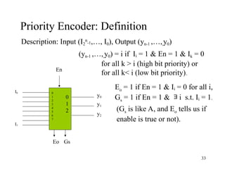
Priority Encoder: Definition
Description: Input (I2
n
-1,…, I0), Output (yn-1 ,…,,y0)
(yn-1 ,…,,y0) = i if Ii = 1 & En = 1 & Ik = 0
for all k > i (high bit priority) or
for all k< i (low bit priority).
Eo = 1 if En = 1 & Ii = 0 for all i,
Gs = 1 if En = 1 & i s.t. Ii = 1.
E
(Gs is like A, and Eo tells us if
enable is true or not).
0
1
2
3
4
5
6
7
En
Eo Gs
I0
I7
y0
y1
y2
0
1
2
34. 34
Priority Encoder: Implement a 32-input priority
encoder w/ 8 input priority encoders (high bit priority).
y32, y31, y30
I31-24
Eo Gs
y22, y21, y20
I25-16
Eo Gs
y12, y11, y10
I15-8
Eo Gs
y02, y01, y00
I7-0
Eo Gs
En
36. • 4 to 2 Priority Encoder Using a For Loop
A signal that is assigned a value multiple
times in an always block retains its last value
priority scheme relies on this for correct
setting of Y and z
43. Shift Registers
• Basic shift registers are classified by
structure according to the following types:
• Serial-in/serial-out
• Parallel-in/serial-out
• Serial-in/parallel-out
• Universal parallel-in/parallel-out
• Ring counter
50. • Machine Arithmetic
– Arithmetic combinational circuits are required for
• Addition
• Subtraction
• Multiplication
• Division (hardware implementation is optional)
– Addition / subtraction can be done easily using full
adders and a minimum of additional logic
51. Addition of Binary Numbers
Full Adder. The full adder is the fundamental building block
of most arithmetic circuits:
The sum and carry outputs are described as:
i
i
i
i
i
i
i
i
i
i
i
i
i
i
i
i
i
i
i c
b
c
a
b
a
c
b
a
c
b
a
c
b
a
c
b
a
c
1
i
i
i
i
i
i
i
i
i
i
i
i
i c
b
a
c
b
a
c
b
a
c
b
a
s
Full
Adder
Cin
Cout
si
ai bi
53. Full-Adder Implementation
Full Adder operations is defined by equations:
i
i
i
i
i
i
i
i
i
i
i
i
i
i
i
i
i
i c
p
c
b
a
c
b
a
c
b
a
c
b
a
c
b
a
s
i
i
i
i
i
i
i
i
i
i
i
i c
p
g
b
a
c
b
a
c
b
a
c
1
One-bit adder could be
implemented as shown
Carry-Propagate:
and Carry-Generate gi
i
i
i b
a
p
i
i
i b
a
g
cout
cin
si
ai bi
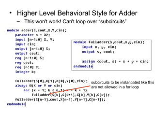
55. • Higher Level Behavioral Style for Adder
– This won't work! Can't loop over “subcircuits”
subcircuits to be instantiated like this
are not allowed in a for loop
56. High-Speed Addition
i
i
i c
p
s
i
i
i
i c
p
g
c
1
One-bit adder could be
implemented more efficiently
because MUX is faster
i
i
i b
a
p
i
i
i b
a
g
0
1
s
bi
ai
cout
si
cin
57. • Ripple-Carry Adder
– A ripple carry adder cascades full adders together
• Simple, but not the most efficient design
• Carry propagate adders are more efficient
FA
xn –1
cn cn 1
-
yn 1
–
sn 1
–
FA
x1
c2
y1
s1
FA
c1
x0 y0
s0
c0
MSB position LSB position
58. The Ripple-Carry Adder
A0 B0
S0
Co,0
Ci,0
A1 B1
S1
Co,1
A2 B2
S2
Co,2
A3 B3
S3
Co,3
(= Ci,1)
FA FA FA FA
Worst case delay linear with the number of bits
tadder N 1
–
tcarry tsum
+
td = O(N)
Goal: Make the fastest possible carry path circuit
From Rabaey
59. Inversion Property
A B
S
Co
Ci FA
A B
S
Co
Ci FA
S A B Ci
S A B Ci
=
Co A B Ci
Co A B Ci
=
From Rabaey
60. Minimize Critical Path by Reducing Inverting
Stages
A0 B0
S0
Co,0
Ci,0
A1 B1
S1
Co,1
A2 B2
S2
Co,2 Co,3
FA’ FA’ FA’ FA’
A3 B3
S3
Odd Cell
Even Cell
Exploit Inversion Property
Note: need 2 different types of cells
From Rabaey
61. Ripple Carry Adder
Carry-Chain of an RCA implemented using multiplexer from the
standard cell library: ai+1 bi+1 ai bi
ai+2
bi+2
cout
ci+1
ci
si
si+1
si+2
cin
Critical Path
Oklobdzija, ISCAS’88
62. • Ripple-Carry Adder Using Generate
compiler produces n modules with names
addstage[0].addbit, addstage[1].addbit, …,
addstage[n-1].addbit
63. Carry Look Ahead Logic (CLA)
i
i
i c
p
s
i
i
i
i c
p
g
c
1
i
i
i b
a
p
i
i
i b
a
g
0
1
s
bi
ai
cout
si
cin
64. CLA Definitions: 4-bit Adder
ai bi
Ci
gi pi
ai+1 bi+1
Ci+1
gi+1 pi+1
ai+2 bi+2
Ci+2
gi+2 pi+2
ai+3 bi+3
Ci+3
gi+3 pi+3
Ci+4
1
1
1
1
1
1
1
1
1
1
2 )
(
c
p
p
g
p
g
c
p
g
p
g
c
p
g
c
i
i
i
i
i
i
i
i
i
i
i
i
i
i
i
i
i
i
i
i
i
i
i
i
i c
p
g
b
a
c
b
a
c
b
a
c
1
65. Carry-Lookahead Adder: 4-bits
ai bi
Ci
gi pi
ai+1 bi+1
Ci+1
gi+1 pi+1
ai+2 bi+2
Ci+2
gi+2 pi+2
ai+3 bi+3
Ci+3
gi+3 pi+3
Ci+4
i
i
i
i
i
i
i
i
i
i
i
i
i
i
i
i
i
i
i
i
i
i
c
p
p
p
g
p
p
g
p
g
c
p
p
g
p
g
p
g
c
p
g
c
1
2
1
2
1
2
2
1
1
1
2
2
2
2
2
3 )
(
i
i
i
i
i
i
i
i
i
i
i
i
i
i
i
i
i
i
i
i
i
i
i
i
i
i
i
c
p
p
p
p
g
p
p
p
g
p
p
g
p
g
g
p
p
g
p
g
p
g
c
p
g
c
1
2
3
1
2
3
1
2
3
2
3
3
1
2
1
2
2
3
3
3
3
3
4 )
(
Gj Pj
66. Carry-Lookahead Adder
i
i
i
i
i
i
i
i
i
i
j g
p
p
p
g
p
p
g
p
g
G 1
2
3
1
2
3
2
3
3
i
i
i
i
j p
p
p
p
P 1
2
3
j
j
j
j c
P
G
c
)
1
(
4
One gate delay
to calculate p, g
One to calculate
P and two for G
Three gate delays
To calculate C4(j+1)
Compare that to 8 in RCA !
ai bi
Cin Cj
Gj
Pj
ai+1 bi+1
gi+1
pi+1 gi pi
ai+2 bi+2
ai+3 bi+3
gi+1pi+1
gi+1pi+1
C4(j+1)
C4j+1
C4j+2
C4j+3
P, G Group
67. Carry-Lookahead Adder
(Weinberger and Smith)
i
i
i
i
i
i
i
i
i
i
j G
P
P
P
G
P
P
G
P
G 1
2
3
1
2
3
2
3
3
*
G
i
i
i
i
j P
P
P
P
P 1
2
3
*
j
k
k
j c
P
G
c 4
)
1
(
4 *
*
Pj
G* P*
C4j+1
Gj
Pj+1
Gj+1
Pj+3
Gj+3
Pj+2
Gj+2
C4j
C4(j+1)
C4j+2
C4j+3
Additional two gate delays
C16 will take a total of 5 vs. 32 for RCA !
70. Carry lookahead addition
• Two ways in which carry=1 from the ith bit-slice
– Generated if both ai and bi are 1
•
– A CarryIn (ci) of 1 is propagated if ai or bi are 1
•
bi
ai
gi
bi
ai
pi
Are these carries generated or propagated?
71. Carry lookahead addition
• Two ways in which carry=1 from the ith bit-slice
– Generated if both ai and bi are 1
•
– A CarryIn (ci) of 1 is propagated if ai or bi are 1
•
• The carry out, ci+1, is therefore
• Using substitution, can get carries in parallel
bi
ai
gi
bi
ai
pi
ci
pi
gi
ci
1
0
0
1
2
3
0
1
2
3
1
2
3
2
3
3
4
0
0
1
2
0
1
2
1
2
2
3
0
0
1
0
1
1
2
0
0
0
1
c
p
p
p
p
g
p
p
p
g
p
p
g
p
g
c
c
p
p
p
g
p
p
g
p
g
c
c
p
p
g
p
g
c
c
p
g
c
.
.
.
72. Carry lookahead addition
• Drawbacks
– n+1 input OR and AND gates for nth
input
– Irregular structure with many long wires
• Solution: do two levels of carry
lookahead
– First level generates Result (using carry
lookahead to generate the internal
carries) and propagate and generate
signals for a group of 4 bits (Pi and Gi)
– Second level generates carry out’s for
each group based on carry in and Pi and
Gi from previous group
73. Carry lookahead addition
• Internal equations for group 0
• Group equations for group 0
• C1 output of carry lookahead unit
bi
ai
gi
bi
ai
pi
ci
pi
gi
ci
1
0
1
2
3
1
2
3
2
3
3
0 g
p
p
p
g
p
p
g
p
g
G
0
1
2
3
0 p
p
p
p
P
0
0
0
1 c
P
G
C
74. Carry lookahead addition
• Internal equations for group 1
• Group equations for group 1
• C2 output of carry lookahead unit
76. Carry-Skip Addition
• CLA group generate (Gi) hardware is complex
• Carry skip addition
– Generate Gi’s by ripple carry of a and b inputs with
cin’s = 0 (except c0)
Generate Pi’s as in carry lookahead
– For each group, combine Gi, Pi, and cin as in carry
lookahead to form group carries
– Generate sums by ripple carry from a and b inputs
and group carries
78. Carry skip addition
• Operation
– Generate Gi’s through ripple carry
– In parallel, generate Pi’s as in carry lookahead
79. Carry skip addition
• Operation
– Group carries to each block are generated or propagated
80. Carry skip addition
• Operation
– Group carries to each block are generated or propagated
– Sums are generated in parallel from group carries
81. Carry-Skip Adder
FA FA FA FA
P0 G1 P0 G1 P2 G2 P3 G3
Co,3
Co,2
Co,1
Co,0
Ci,0
FA FA FA FA
P0 G1 P0 G1 P2 G2 P3 G3
Co,2
Co,1
Co,0
Ci,0
Co,3
Multiplexer
BP=PoP1P2P3
Idea: If (P0 and P1 and P2 and P3 = 1)
then Co3 = C0, else “kill” or “generate”.
Bypass
From Rabaey
82. Carry-Skip Adder:
N-bits, k-bits/group, r=N/k groups
Gr
G r-
1
...
S
N-k-1
SN-1
a N-1bN-1 b N-k-1
aN-k-1
S (r-1)k-1 S (r-2)k
G1
Go
...
Sk
S
2k-1
a 2k-1
b 2k-1 bk
ak
S
k-1
S
0
...
...
a (r-1)k
b(r-1)k a (r-1)kb (r-1)k
...
a k-1
b k-1
a0 b0
...
Cin
... ... ... ... ... ... ... ...
Pr-1
Pr-2 P1 P0
Cout + + + +
AND
OR
OR
OR OR
AND
AND
AND
critical path, delay =2(k-1)+(N/2-2)
83. Carry-Skip Adder
SKIP
RCA
d t
N
t
k
t
2
2
1
2
N
tp
ripple adder
bypass adder
4..8
k
84. Carry-Select Addition
• For each group, do two additions in parallel
– One with cin forced to 0
– One with cin forced to 1
• Generate cin in parallel and use a MUX to select the
correct sum outputs
• Example for 8 bits
MUXes
85. Carry-select addition
• A larger design
– Why different numbers of bits in each block?
• Hint1: it’s to minimize the adder delay
• Hint2: assume a k-input block has k time units of delay, and the
AND- OR logic has 1 time unit of delay
generated carry
propagated carry
89. Carry Save Addition
• A full adder sums 3 inputs and produces 2 outputs
– Carry output has twice weight of sum output
• N full adders in parallel are called carry save adder
– Produce N sums and N carry outs
Z4
Y4
X4
S4
C4
Z3
Y3
X3
S3
C3
Z2
Y2
X2
S2
C2
Z1
Y1
X1
S1
C1
XN...1
YN...1
ZN...1
SN...1
CN...1
n-bit CSA
90. CSA Application
• Use k-2 stages of CSAs
– Keep result in carry-save redundant form
• Final CPA computes actual result
4-bit CSA
5-bit CSA
0001 0111 1101 0010
+
1011
0101_
0001
0111
+1101
1011
0101_
X
Y
Z
S
C
0101_
1011
+0010
X
Y
Z
S
C
A
B
S
91. CSA Application
• Use k-2 stages of CSAs
– Keep result in carry-save redundant form
• Final CPA computes actual result
4-bit CSA
5-bit CSA
0001 0111 1101 0010
+
1011
0101_
01010_ 00011
0001
0111
+1101
1011
0101_
X
Y
Z
S
C
0101_
1011
+0010
00011
01010_
X
Y
Z
S
C
01010_
+ 00011
A
B
S
92. CSA Application
• Use k-2 stages of CSAs
– Keep result in carry-save redundant form
• Final CPA computes actual result
4-bit CSA
5-bit CSA
0001 0111 1101 0010
+
1011
0101_
01010_ 00011
0001
0111
+1101
1011
0101_
X
Y
Z
S
C
0101_
1011
+0010
00011
01010_
X
Y
Z
S
C
01010_
+ 00011
10111
A
B
S
10111
99. Multiplication
• Example:
• M x N-bit multiplication
– Produce N M-bit partial products
– Sum these to produce M+N-bit product
1100 : 1210
0101 : 510
1100
0000
1100
0000
00111100 : 6010
multiplier
multiplicand
partial
products
product
100. General Form
• Multiplicand: Y = (yM-1, yM-2, …, y1, y0)
• Multiplier: X = (xN-1, xN-2, …, x1, x0)
• Product:
1 1 1 1
0 0 0 0
2 2 2
M N N M
j i i j
j i i j
j i i j
P y x x y
x0
y5
x0
y4
x0
y3
x0
y2
x0
y1
x0
y0
y5
y4
y3
y2
y1
y0
x5 x4 x3 x2 x1 x0
x1
y5
x1
y4
x1
y3
x1
y2
x1
y1
x1
y0
x2
y5
x2
y4
x2
y3
x2
y2
x2
y1
x2
y0
x3
y5
x3
y4
x3
y3
x3
y2
x3
y1
x3
y0
x4
y5
x4
y4
x4
y3
x4
y2
x4
y1
x4
y0
x5y5 x5y4 x5y3 x5y2 x5y1 x5y0
p0
p1
p2
p3
p4
p5
p6
p7
p8
p9
p10
p11
multiplier
multiplicand
partial
products
product
101. Dot Diagram
• Each dot represents a bit
partial products
multiplier
x
x0
x15
104. Fewer Partial Products
• Array multiplier requires N partial products
• If we looked at groups of r bits, we could
form N/r partial products.
– Faster and smaller?
– Called radix-2r
encoding
• Ex: r = 2: look at pairs of bits
– Form partial products of 0, Y, 2Y, 3Y
– First three are easy, but 3Y requires adder
105. Booth Encoding
• Instead of 3Y, try –Y, then increment next
partial product to add 4Y
• Similarly, for 2Y, try –2Y + 4Y in next
partial product
106. Booth Encoding
• Instead of 3Y, try –Y, then increment next
partial product to add 4Y
• Similarly, for 2Y, try –2Y + 4Y in next
partial product
107. Booth Encoding
• Instead of 3Y, try –Y, then increment next
partial product to add 4Y
• Similarly, for 2Y, try –2Y + 4Y in next
partial product
108. Booth Encoding
• Instead of 3Y, try –Y, then increment next
partial product to add 4Y
• Similarly, for 2Y, try –2Y + 4Y in next
partial product
109. Booth Encoding
• Instead of 3Y, try –Y, then increment next
partial product to add 4Y
• Similarly, for 2Y, try –2Y + 4Y in next
partial product
110. Booth Encoding
• Instead of 3Y, try –Y, then increment next
partial product to add 4Y
• Similarly, for 2Y, try –2Y + 4Y in next
partial product
111. Booth Encoding
• Instead of 3Y, try –Y, then increment next
partial product to add 4Y
• Similarly, for 2Y, try –2Y + 4Y in next
partial product
112. Booth Encoding
• Instead of 3Y, try –Y, then increment next
partial product to add 4Y
• Similarly, for 2Y, try –2Y + 4Y in next
partial product
113. Booth Hardware
• Booth encoder generates control lines for
each PP
– Booth selectors choose PP bits
Mi
yj
Xi
yj-1
2Xi
PPij
Booth
Selector
Booth
Encoder
x2i+1
x2i
x2i-1
114. Sign Extension
• Partial products can be negative
– Require sign extension, which is cumbersome
– High fanout on most significant bit
multiplier
x
x0
x15
0
0
0
x-1
x16
x17
s
s
s
s
s
s
s
s
s
s
s
s
s
s
s
s
s
s
s
s
s
s
s
s
s
s
s
s
s
s
s
s
s
s
s
s
s
s
s
s
s
s
s
s
s
s
s
s
s
s
s
s
s
s
s
s
s
s
s
s
s
s
s
s
s
s
s
s
s
s
s
s
PP0
PP1
PP2
PP3
PP4
PP5
PP6
PP7
PP8
115. Simplified Sign Ext.
• Sign bits are either all 0’s or all 1’s
– Note that all 0’s is all 1’s + 1 in proper column
– Use this to reduce loading on MSB
s
1
1
1
1
1
1
1
1
1
1
1
1
1
1
1
s
s
1
1
1
1
1
1
1
1
1
1
1
1
1
s
s
1
1
1
1
1
1
1
1
1
1
1
s
s
1
1
1
1
1
1
1
1
1
s
s
1
1
1
1
1
1
1
s
s
1
1
1
1
1
s
s
1
1
1
s
s
1
s
PP0
PP1
PP2
PP3
PP4
PP5
PP6
PP7
PP8
116. Even Simpler Sign Ext.
• No need to add all the 1’s in hardware
– Precompute the answer!
s
s
s
s
s
s
1
s
s
1
s
s
1
s
s
1
s
s
1
s
s
1
s
s
PP0
PP1
PP2
PP3
PP4
PP5
PP6
PP7
PP8
#51: Digital computer arithmetic is an aspect of logic design with the objective of developing appropriate algorithms in order to achieve an efficient utilization of the available hardware. Given that the hardware can only perform relatively simple and primitive set of Boolean operations, arithmetic operations are based on a hierarchy of operations that are built upon the simple ones. Since ultimately, speed, power and chip area are the most often used measures of the efficiency of an algorithm, there is a strong link between the algorithms and technology used for its implementation.
#52: Digital computer arithmetic is an aspect of logic design with the objective of developing appropriate algorithms in order to achieve an efficient utilization of the available hardware. Given that the hardware can only perform relatively simple and primitive set of Boolean operations, arithmetic operations are based on a hierarchy of operations that are built upon the simple ones. Since ultimately, speed, power and chip area are the most often used measures of the efficiency of an algorithm, there is a strong link between the algorithms and technology used for its implementation.
#53: First we should examine a realization of a one-bit adder which represents a basic building block for all the more elaborate addition schemes.
Operation of a Full Adder is defined by the Boolean equations for the sum and carry signals shown in this slide: ai, bi, and ci are the inputs to the i-th full adder stage, and si and ci+1 are the sum and carry outputs from the i-th stage, respectively.
From the above equation it is clear that the realization of the Sum function requires two XOR logic gates.
The expression for Carry function could be rewritten using the Carry-Propagate pi and Carry-Generate gi terms.
If Carry-Propagate is 1, the Carry out of the stage will be equal to the Carry signal into the stage: ci+1 = ci regardless of the carry inside the stage.
If Carry-Generate is 1, there will be a Carry signal out of the stage will be 1 regardless of the value of the incoming Carry signal.
The logical implementation of the full adder stage is shown in figure (a.) of this slide. This implementation results from a direct application of the logic equations.
The implementation (b) is more clever because it utilizes a multiplexer in the carry path. Given that the multiplexer block is often faster than a single gate, using multiplexer in the critical path helps to achieve better performance.
#56: First we should examine a realization of a one-bit adder which represents a basic building block for all the more elaborate addition schemes.
Operation of a Full Adder is defined by the Boolean equations for the sum and carry signals shown in this slide: ai, bi, and ci are the inputs to the i-th full adder stage, and si and ci+1 are the sum and carry outputs from the i-th stage, respectively.
From the above equation it is clear that the realization of the Sum function requires two XOR logic gates.
The expression for Carry function could be rewritten using the Carry-Propagate pi and Carry-Generate gi terms.
If Carry-Propagate is 1, the Carry out of the stage will be equal to the Carry signal into the stage: ci+1 = ci regardless of the carry inside the stage.
If Carry-Generate is 1, there will be a Carry signal out of the stage will be 1 regardless of the value of the incoming Carry signal.
The logical implementation of the full adder stage is shown in figure (a.) of this slide. This implementation results from a direct application of the logic equations.
The implementation (b) is more clever because it utilizes a multiplexer in the carry path. Given that the multiplexer block is often faster than a single gate, using multiplexer in the critical path helps to achieve better performance.
#61: A ripple carry adder for N-bit numbers is implemented by concatenating N full adders as shown in this slide. At the i-th bit position, the i-th bits of operands A and B and a carry signal from the preceding adder stage are used to generate the i-th bit of the sum, si, and a carry, ci+1, to the next adder stage. This scheme is called a Ripple Carry Adder, since the carry signal “ripple” from the least significant bit position to the most significant one. If the ripple carry adder is implemented by concatenating N full adders, the delay of such an adder is 2N gate delays from Cin-to-Cout.
The path from the input to the output signal that is likely to take the longest time is designated as a "critical path". In the case of a Ripple Carry Adder, this is the path from the least significant input a0 or b0 to the last sum bit sn. Assuming multiplexer based XOR gate implementation, this critical path will consist of N+1 pass transistor delays. However, such a long chain of transistors will significantly degrade the signal, thus some amplification points are necessary. In practice, we can use a multiplexer cell to build this critical path using standard cell library as shown in this slide.
#63: First we should examine a realization of a one-bit adder which represents a basic building block for all the more elaborate addition schemes.
Operation of a Full Adder is defined by the Boolean equations for the sum and carry signals shown in this slide: ai, bi, and ci are the inputs to the i-th full adder stage, and si and ci+1 are the sum and carry outputs from the i-th stage, respectively.
From the above equation it is clear that the realization of the Sum function requires two XOR logic gates.
The expression for Carry function could be rewritten using the Carry-Propagate pi and Carry-Generate gi terms.
If Carry-Propagate is 1, the Carry out of the stage will be equal to the Carry signal into the stage: ci+1 = ci regardless of the carry inside the stage.
If Carry-Generate is 1, there will be a Carry signal out of the stage will be 1 regardless of the value of the incoming Carry signal.
The logical implementation of the full adder stage is shown in figure (a.) of this slide. This implementation results from a direct application of the logic equations.
The implementation (b) is more clever because it utilizes a multiplexer in the carry path. Given that the multiplexer block is often faster than a single gate, using multiplexer in the critical path helps to achieve better performance.
#82: Since the Cin-to-Cout represents the longest path in the ripple-carry-adder an obvious attempt is to accelerate carry propagation through the adder. This is accomplished by using Carry-Propagate pi signals within a group of bits. If all the pi signals within the group are set to pi = 1, the condition exist for the carry to bypass the entire group:
Carry Skip Adder divides the words to be added into groups of equal size of k-bits.
The basic structure of an N-bit Carry Skip Adder is shown here. Within the group, carry propagates in a ripple-carry fashion. In addition, an AND gate is used to form the group propagate signal. If group propagate signal is “true” the condition exists for carry to bypass, the group as shown in this slide.
The maximal delay of a Carry Skip Adder is encountered when carry signal is generated in the least-significant bit position, rippling through k-1 bit positions, skipping over N/k-2 groups in the middle, rippling through the k-1 bits of most significant group and being assimilated in the Nth bit position to produce the sum SN:
Thus, Carry Skip Adder is faster than Ripple Carry Adder at the expense of a few relatively simple modifications. The delay of the Carry Skip Adder is still linearly dependent on the size of the adder N, however this linear dependence is reduced by a factor of 1/k.
#87: The theoretically fastest scheme for addition of two numbers is "Conditional-Sum Addition" proposed by Sklansky in 1960. The essence of this scheme is in the realization that we can add two numbers without waiting for the carry signal to arrive.
Simply, the numbers are added in two instances: one assuming Cin = 0 and the other assuming Cin = 1. The conditionally produced results: Sum0, Sum1 and Carry0, Carry1 are selected by a multiplexer using an incoming carry signal Cin as a multiplexer control.
Similarly to the Carry-Lookahead Adder the input bits are divided into groups which are in this case added "conditionally".
It is apparent that while building Conditional-Sum Adder the hardware complexity starts to grow rapidly starting from the Least Significant Bit position. Therefore, in practice, the full-blown implementation of the CNSA is not found.
However, the idea of adding the Most Significant portion of the operands conditionally and selecting the results once the carry-in signal is computed in the Least Significant portion, is attractive. Such a scheme, which is a subset of Conditional-Sum Adder, is known as "Carry-Select Adder".
Carry Select Adder divides the words to be added into blocks and forms two sums for each block in parallel:
-one with a carry in of ZERO and the other with a carry in of ONE.
In this slide an example of a 16 bit carry select adder in shown:
The carry-out from the Least Significant 4-bit block controls a multiplexer that selects the sum from the Most Significant portion. The carry out is computed using the equation for the carry out of the group, since the group propagate signal Pi is the carry out of an adder with a carry input of ONE and the group generate Gi signal is the carry out of an adder with a carry input of ZERO.
This speeds-up the computation of the carry signal which is necessary for selection in the next block.
The upper 8-bits are computed conditionally using two Carry-Select Adders similar to the one used in the Least Significant 8-bit portion.
The delay of this adder is determined by the speed of the Least Significant k-bit block (4-bit RCA in this example) and delay of multiplexers in the Most Significant path.
Generally the delay of such adder is proportional to the log function of the size of the adder.


![• Verilog: 4x1 MUX (Data Flow Style)
– This is getting complicated!
– Need a way to specify a “group” of bits like w[0:3]
– Need a way to replace ?: with “if then else”](https://image.slidesharecdn.com/unitiv-250430175943-93aa84d0/85/ME-applied-electronics-Vlsi-UNIT-IV-ppt-12-320.jpg)
![• Vectored Signals in Verilog
Signals can be grouped as bit vectors
• The order of the bits is user determined
• W has 4 lines with the MSB = W[0] and the LSB = W[3]
• S has two lines with the MSB = S[1] and the LSB = S[0]
Format is [MSB:LSB]](https://image.slidesharecdn.com/unitiv-250430175943-93aa84d0/85/ME-applied-electronics-Vlsi-UNIT-IV-ppt-13-320.jpg)


![• Ripple-Carry Adder Using Generate
compiler produces n modules with names
addstage[0].addbit, addstage[1].addbit, …,
addstage[n-1].addbit](https://image.slidesharecdn.com/unitiv-250430175943-93aa84d0/85/ME-applied-electronics-Vlsi-UNIT-IV-ppt-62-320.jpg)