


![EXAMPLE-4 Consider a system in which the 64kb memory space is implemented using eight numbers of 8kb memory. Interface the EPROM and RAM with 8085 processor. The total memory capacity is 64Kb. So, let 3 numbers of 8Kb EPROM and 5 numbers of 8Kb RAM. Each 8kb memory requires 13 address lines. So the address line A0 - A12 of the processor are connected to 13address pins of all the memory lCs. The address lines A13, A14 and A]5 are decoded using a 3-to-8 coder to generate eight chip select signals. These eight chip select signals can be used to select one of the eight memories at any one time.](https://image.slidesharecdn.com/memoryintrfaceandaddrsmodes-110122042346-phpapp02/85/Memory-intrface-and-addrs-modes-19-320.jpg)


Memory intrface and addrs modes
- 1. By : Balbir Virdi
- 3. Instruction cycle Instruction cycle is defined as the time required to complete the execution of an instruction. 8085 instruction cycle consist of one to six machine cycle or one to six operation. Machine cycle is defined as the time required to complete one operation of accessing memory, I/O or Acknowledging an external request. This cycle may consist of three to six T cycle. T-state is defined as one subdivision of the operation performed in one clock period . Each T-state is precisely equal to one clock period. These two terms are often used synonymously.
- 4. Memory is made up of semiconductor material used to store the programs and data. Three types of memory is, Process memory Primary or main memory Secondary memory
- 5. EPROM AND STATIC RAM: Typical semiconductor memory IC will have n address pins, m data pins (or output pins). Having two power supply pins (one for connecting required supply voltage (V and the other for connecting ground). The control signals needed for static RAM are chip select (chip enable), read control (output enable) and write control (write enable). The control signals needed for read operation in EPROM are chip select (chip enable) and read control (output enable).
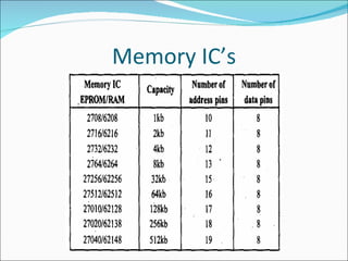
- 6. Memory IC’s
- 7. DECODER It is used to select the memory chip of processor during the execution of a program. No. of IC's used for decoder is, 2-4 decoder (74LS139) 3-8 decoder (74LS138)
- 10. Consider a system in which the full memory space 64kb is utilized for EPROM memory. Interface the EPROM with 8085 processor. The memory capacity is 64 Kbytes. i.e. 2^n = 64 x 1000 bytes where n = address lines. So, n = 16. In this system the entire 16 address lines of the processor are connected to address input pins of memory IC in order to address the internal locations of memory. The chip select (CS) pin of EPROM is permanently tied to logic low (i.e., tied to ground). Since the processor is connected to EPROM, the active low RD pin is connected to active low output enable pin of EPROM. The range of address for 64 Kbytes EPROM is 0000H to FFFFH.
- 11. Consider a system in which the full memory space 64kb is utilized for EPROM memory. Interface the EPROM with 8085 processor. The memory capacity is 64 Kbytes. i.e. 2^n = 64 x 1000 bytes where n = address lines. So, n = 16.
- 12. In this system the entire 16 address lines of the processor are connected to address input pins of memory IC in order to address the internal locations of memory. The chip select (CS) pin of EPROM is permanently tied to logic low (i.e., tied to ground). Since the processor is connected to EPROM, the active low RD pin is connected to active low output enable pin of EPROM. The range of address for 64 Kbytes EPROM is 0000H to FFFFH.
- 13. EXAMPLE 2 Consider a system in which the available 64kb memory space is equally divided between EPROM and RAM. Interface the EPROM and RAM with 8085 processor.
- 14. The 32kb memory requires 15 address lines and so the address lines A0 - A14 of the processor are connected to 15 address pins of both EPROM and RAM. The unused address line A15 is used as to chip select. If A15 is 1, it select RAM and If A15 is 0, it select EPROM. Inverter is used for selecting the memory. The memory used is both Ram and EPROM, so the low RD and WR pins of processor are connected to low WE and OE pins of memory respectively. The address range of EPROM will be 0000H to 7FFFH and that of RAM will be 8000H to FFFFH.
- 15. EXAMPLE-3 Consider a system in which 32kb memory space is implemented using four numbers of 8kb memory. Interface the EPROM and RAM with 8085 processor.
- 17. The total memory capacity is 32Kb. So, let two number of 8kb n memory be EPROM and the remaining two numbers be RAM. Each 8kb memory requires 13 address lines and so the address lines A0- A12 of the processor are connected to 13 address pins of all the memory. The address lines and A13 - A14 can be decoded using a 2-to-4 decoder to generate four chip select signals. These four chip select signals can be used to select one of the four memory IC at any one time. The address line A15 is used as enable for decoder.
- 18. The address allotted to each memory IC is shown in following table.
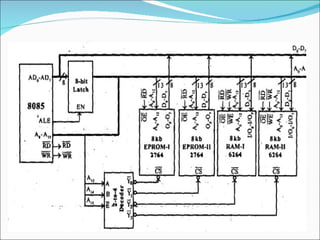
- 19. EXAMPLE-4 Consider a system in which the 64kb memory space is implemented using eight numbers of 8kb memory. Interface the EPROM and RAM with 8085 processor. The total memory capacity is 64Kb. So, let 3 numbers of 8Kb EPROM and 5 numbers of 8Kb RAM. Each 8kb memory requires 13 address lines. So the address line A0 - A12 of the processor are connected to 13address pins of all the memory lCs. The address lines A13, A14 and A]5 are decoded using a 3-to-8 coder to generate eight chip select signals. These eight chip select signals can be used to select one of the eight memories at any one time.
- 22. Programming model Programming model is a conceptual representation of a real object. It can take any form, such as text description, a drawing, or a built structure. Like the architecture model of a building, microprocessor can be represented in terms of its physical electronic components and information needed to write programs. The programming model consist of some segments of the ALU and the registers.
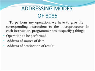
- 24. ADDRESSING MODES OF 8085 To perform any operation, we have to give the corresponding instructions to the microprocessor. In each instruction, programmer has to specify 3 things: Operation to be performed. Address of source of data. Address of destination of result.
- 25. The method by which the address of source of data or the address of destination of result is given in the instruction is called Addressing Modes. The term addressing mode refers to the way in which the operand of the instruction is specified.
- 26. Types of Addressing Modes Intel 8085 uses the following addressing modes: 1. Direct Addressing Mode 2. Register Addressing Mode 3. Register Indirect Addressing Mode 4. Immediate Addressing Mode 5. Implicit Addressing Mode
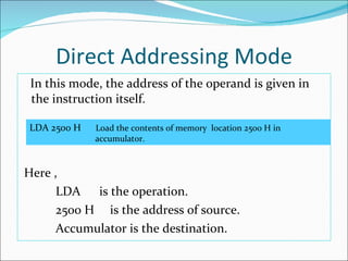
- 27. Direct Addressing Mode In this mode, the address of the operand is given in the instruction itself. Here , LDA is the operation. 2500 H is the address of source. Accumulator is the destination. LDA 2500 H Load the contents of memory location 2500 H in accumulator.
- 28. Register Addressing Mode In this mode, the operand is in general purpose register. MOV is the operation. B is the source of data. A is the destination. MOV A, B Move the contents of register B to A.
- 29. Register Indirect Addressing Mode In this mode, the address of operand is specified by a register MOV is the operation. M is the memory location specified by H-L register pair. A is the destination register pair. MOV A, M Move data from memory location specified by H-L pair to accumulator.
- 30. Immediate Addressing Mode In this mode, the operand is specified within the instruction itself. MVI is the operation. 05 H is the immediate data (source). A is the destination. MVI A, 05 H Move 05 H in accumulator.
- 31. Implicit Addressing Mode If address of source of data as well as address of destination of result is fixed, then there is no need to give any operand along with the instruction. CMA is the operation. A is the source. A is the destination. CMA Complement accumulator.