Memory mapping techniques and low power memory design
Download as PPTX, PDF9 likes2,866 views

This document discusses memory mapping techniques and low power memory design. It describes three main memory mapping techniques: direct mapping, fully-associative mapping, and set-associative mapping. It then discusses a proposed method for low power off-chip memory design for video decoders using an embedded bus-invert coding scheme. The method aims to minimize power consumption of external memory in an efficient way without increasing algorithm complexity or requiring system modifications.


Memory mapping techniques and low power memory design
- 1. Memory Mapping Techniques and Low Power Memory Design Presented By: Babar Shahzaad 14F-MS-CP-12 Department of Computer Engineering , Faculty of Telecommunication and Information Engineering , University of Engineering and Technology (UET), Taxila
- 2. Outline Memory Mapping Techniques Direct Mapping Fully-Associative Mapping Set-Associative Mapping Summary of Memory Mapping Techniques Low-Power Off-Chip Memory Design for Video Decoder Using Embedded Bus-Invert Coding
- 4. Memory Mapping Techniques There are three main types of memory mapping techniques: 1. Direct Mapping 2. Fully-Associative Mapping 3. Set-Associative Mapping For the coming explanations, let us assume 1GB main memory, 128KB Cache Memory and Cache Line Size 32B
- 6. Direct Mapping Each block of main memory maps to only one cache line i.e. if a block is in cache, it must be in one specific place Address is in two parts Least Significant w bits identify unique word/byte Most Significant s bits specify one memory block The MSBs are split into a cache line field r and a tag of s-r (most significant)
- 7. Direct Mapping (Cont…) TAG LINE or SLOT(r) OFFSET S W For the given example, we have: 1GB Main Memory = 220 bytes Cache Size = 128KB = 217 bytes Block Size = 32B = 25 bytes No. of Cache Line = 217/ 25 = 212 , thus 12 bits are required to locate 212 lines
- 8. Direct Mapping (Cont…) Also, offset is 25 bytes and thus 5 bits are required to locate individual byte Thus Tag bits = 32 – 12 – 5 = 15 bits 15 12 5
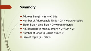
- 9. Summary Address Length = (s + w) bits Number of Addressable Units = 2s+w words or bytes Block Size = Line Size = 2w words or bytes No. of Blocks in Main Memory = 2s+w/2w = 2s Number of Lines in Cache = m = 2r Size of Tag = (s – r) bits
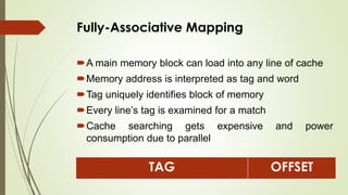
- 11. Fully-Associative Mapping A main memory block can load into any line of cache Memory address is interpreted as tag and word Tag uniquely identifies block of memory Every line’s tag is examined for a match Cache searching gets expensive and power consumption due to parallel TAG OFFSET
- 12. Fully-Associative Mapping (Cont…) For the given example, we have: 1GB Main Memory = 220 bytes Cache Size = 128KB = 217 bytes Block Size = 32B = 25 bytes Here, offset is 25 bytes and thus 5 bits are required to locate individual byte Thus Tag bits = 32 – 5 = 27 bits 27 5
- 13. Summary Address Length = (s + w) bits Number of Addressable Units = 2s+w words or bytes Block Size = Line Size = 2w words or bytes No. of Blocks in Main Memory = 2s+w/2w = 2s Number of Lines in Cache = Total Number of Cache Blocks Size of Tag = s bits
- 15. Set-Associative Mapping Cache is divided into a number of sets Each set contains a number of lines A given block maps to any line in a given set e.g. Block B can be in any line of set i If 2 lines per set 2 way set associative mapping A given block can be in one of 2 lines in only one set TAG SET(d) OFFSET S W
- 16. Set-Associative Mapping(Cont…) For the given example, we have: 1GB Main Memory = 220 bytes Cache Size = 128KB = 217 bytes Block Size = 32B = 25 bytes Let be a 2-way Set Associative Cache No. of Sets = 217/ (2*25)= 211 , thus 11 bits are required to locate 211 sets and each set containing 2 lines
- 17. Set-Associative Mapping(Cont…) Also, offset is 25 bytes and thus 5 bits are required to locate individual byte Thus Tag bits = 32 – 11 – 5 = 16 bits 16 11 5
- 18. Summary Address Length = (s + w) bits Number of Addressable Units = 2s+w words or bytes Block Size = Line Size = 2w words or bytes No. of Blocks in Main Memory = 2s+w/2w = 2s Number of Lines in Set = k Number of Sets = v = 2d Number of Lines in Cache = k*v = k * 2d Size of Tag = (s-d) bits
- 19. Summary of Memory Mapping Techniques Number of Misses Direct Mapping > Set-Associative Mapping > Full- Associative Mapping Access Latency Direct Mapping < Set-Associative Mapping < Full- Associative Mapping
- 20. Low-Power Off-Chip Memory Design for Video Decoder Using Embedded Bus-Invert Coding
- 21. Abstract Simple, efficient and low power memory design proposed Exploits features of DRAM memory and video application Overcomes the drawbacks of the algorithm complexity and system modification of embedded compression Integration of scheme into video decoder Simple bus-invert encoding scheme Fault tolerance of human eyes and lossy processing of video decoding application
- 22. Introduction High Definition(HD) video applications Computation optimized Memory system is still a problem An external SDRAM chip is always needed for the video codec The external memory power consumption is a bottleneck of video decoder system
- 24. Introduction (Cont…) Minimizing the power consumption of the external memory is the key issue for the embedded video application To decrease the power consumption of off-chip memory: The most popular way is embedded compression Two drawbacks: 1. Algorithm complexity 2. System modification
- 25. SDRAM Memory
- 26. Proposed Method
- 31. Conclusion A simple, efficient, low power SDRAM design is proposed in video coding applications Firstly, it exploits the features of power consumption of off- chip SDRAM memory Secondly, the analysis of video decoding is provided Thirdly, this scheme is easy to be integrated into complete video coding system