


![ TIMER MODES OF OPERATION
Timers of 8051:• 8051 has 2, 16-bit Up Counters T1 and T0.
• If the counter counts internal clock pulses it is known as timer.
• If it counts external clock pulses it is known as counter.
• Each counter is divided into 2, 8-bit registers TH1 - TL1 and TH0 - TL0.
• The timer action is controlled mainly by the TCON and the TMOD registers.
TCON - Timer Control (SFR) [Bit-Addressable As TCON.7 to TCON.0]
TF1 and TF0: (Timer Overflow Flag)
• Set (1) when Timer 1 or Timer 0 overflows respectively i.e. its bits roll over from all 1's to all 0's.
• Cleared (0) when the processor executes ISR (address 001BH for Timer 1 and 000BH for Timer 0).
TR1 and TR0: (Timer Run Control Bit)
• Set (1) - Starts counting on Timer 1 or Timer 0 respectively.
• Cleared (0) - Halts Timer 1 or Timer 0 respectively.
IE1 and IE0: (External Interrupt Edge Flag) Set (1) when external interrupt signal received at INT1 or
INT0 respectively. Cleared (0) when ISR executed (address 0013H for Timer 1 and 0003H for Timer 0)
IT1 and IT0: (External Interrupt Type Control Bit)
• Set (1) - Interrupt at INT1 or INT0 must be -ve edge triggered. Cleared (0) - Interrupt at INT1 or
INT0 must be low-level triggered.](https://image.slidesharecdn.com/mpmcpptr20-250130054036-199969d1/85/Microprocessors-Microcomputers-and-Assembly-Language-Microprocessor-Architecture-and-Microcomputer-Systems-78-320.jpg)
![TMOD - Timer Mode Control (SFR) [NOT Bit-Addressable]
C/T: (Counter/Timer)
•Set (1) - Acts as Counter (Counts external frequency on T1 and T0
pin inputs).
•Cleared (0) - Acts as Timer (Counts internal clock frequency,
fosc/12).
Gate: (Gate Enable Control bit)
•Set (1) - Timer controlled by hardware i.e. INTX signal.
•Cleared (0) – Counting independent of INTX signal.
M1, M0: (Mode Selection bits)
Used to select the operational](https://image.slidesharecdn.com/mpmcpptr20-250130054036-199969d1/85/Microprocessors-Microcomputers-and-Assembly-Language-Microprocessor-Architecture-and-Microcomputer-Systems-79-320.jpg)


Microprocessors, Microcomputers and Assembly Language, Microprocessor Architecture and Microcomputer Systems
- 1. Department of Electronics & Communication Engineering UNIT-I Microprocessors, Microcomputers and Assembly Language, Microprocessor Architecture and Microcomputer Systems
- 2. COURSE OBJECTIVES The objectivesof thiscourse: 1. To understand the basic architecture of computer, evolution, and its applications 2. To learn the architectures of Microprocessor and Microcontroller 3. To learn the programming of Microprocessors and Microcontrollers using their programming model 4. To learn the interfacing of memory, I/O, sensors and actuators to microprocessors and microcontrollers
- 3. COURSE OUTCOMES On successful completion of this course, the student will be able 1. Understand the evolution of computers, processors, and its applications 2. Explain the various software and hardware parts of a microprocessors and computer 3. Understand the architectures of 8085,8086 microprocessors and 8051 microcontroller system 4. Analyze the programming model of 8085,8086 Microprocessors & 8051 microcontroller development environment. 5. Implement the techniques of interfacing memories, various I/O devices, sensors and actuators with microprocessor and microcontrollers 6. Design and develop various microprocessor/microcontroller- based systems for the real-life problems
- 4. Content ➢Microprocessors ➢Microprocessor instruction set and computer languages ➢From large computers to single chip microcontrollers ➢Application: Microprocessor controlled temperature system (MCTS) ➢Microprocessor Architecture and Microcomputer Systems: ➢Microprocessor Architecture and its operation Memory ➢Input and output devices ➢Example of a microcomputer system
- 5. MICROPROCESSOR •Microprocessor is a small chip Part to control functions of digital systems like music players, electronic calculators, computers and others. (OR) •A microprocessor is a component that performs the instructions and task involved in computer processing. (OR) •An integrated circuit that contains all the functions of a central processing unitof a computer.
- 7. 8 Microprocessortypes 🠶 Microprocessors can be characterized based on 🠶 the word size 🠶 4bit(4004),8bit (8085 ), 16 bit(8086), 32 bit(80386,80486), 64 bit(intel core i3,i5,i7) etc. 🠶 Instruction set structure 🠶 RISC (Reduced Instruction Set Computer), CISC (Complex Instruction Set Computer) 🠶 Functions 🠶 General purpose, special purpose such image processing, floating point calculations 🠶 And more …
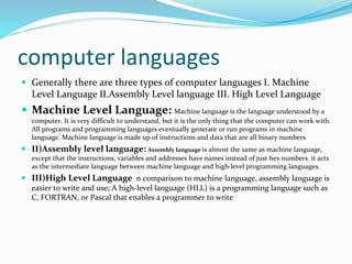
- 8. computer languages Generally there are three types of computer languages I. Machine Level Language II.Assembly Level language III. High Level Language Machine Level Language: Machine language is the language understood by a computer. It is very difficult to understand, but it is the only thing that the computer can work with. All programs and programming languages eventually generate or run programs in machine language. Machine language is made up of instructions and data that are all binary numbers II)Assembly level language: Assembly language is almost the same as machine language, except that the instructions, variables and addresses have names instead of just hex numbers. it acts as the intermediate language between machine language and high-level programming languages. III)High Level Language n comparison to machine language, assembly language is easier to write and use; A high-level language (HLL) is a programming language such as C, FORTRAN, or Pascal that enables a programmer to write
- 9. CLASSIFICATION OF COMPUTERS FROM LARGE COMPUTERS TO SINGLE CHIP MICROCONTROLLERS: Computers are classified into mainly three types i)Large Computers ii). Medium size Computers iii). Microcomputers i)Large computers Large computers are multipurpose, multiuser, multitasking computers. These are used in computer scientific and engineering calculations, handle large records for large corporations and government agencies. Large computers are two types 1) Main frames and 2) Super computers Main frames A mainframe computer (as storage for large database and serve as maximum number of users simultaneously) is a computer used primarily by large organizations for critical applications, bulk data processing such as the census and industry and consumer statistics, enterprise resource planning, and large- scale transaction processing Super computers Super computers (large and complex mathematical Computations)are fastest high-performance systems available at any given time. Such computers have been used primarily for scientific and engineering work requiring exceedingly high- speed computations.
- 10. ii)Medium size computers (Minicomputers support more than 100 users at a time with multi terminal and time sharing) Medium-size computer systems provide faster operating speeds and larger storage capacities than minicomputer systems. They can support a large number of high-speed input/output devices and several disk drives can be used to provide online access to large data files as required for direct access processing and their operating systems also support both multiprogramming and virtual storage. iii)Microcomputers A microcomputer is a complete computer on a small scale, designed for use by one person at a time. microcomputer is now primarily called a personal computer (PC), or a device based on a single-chip microprocessor. Common microcomputers include laptops and desktops. PERSONAL COMPUTERS (PC) These microcomputers are single-user systems and are used for a variety of purposes, such as payroll, business accounts, word processing, legal and medical record keeping, personal finance, accessing Internet resources (e-mail. Web search, newsgroup), and instruction. They are also known as personal computers (PC) or desktop computers. Typically, the price ranges from $500 to $5000 for a single-user system. Examples include such microcomput- ers as the IBM Personal Computer (Aptiva series), the Hewlett-Packard Pavilion series, and the Apple Macintosh series. At the low end of the microcomputer spectrum, a typical configuration includes a 32- bit (or 64- bit) microprocessor, 32 to 256 MB (megabytes) of system memory, a video screen (monitor), a 3" high-density floppy disk, a hard disk with storage capacity of more than 10 gigabytes, a CDROM, and a Zip disk.
- 11. SINGLE-BOARD MICROCOMPUTERS These microcomputers are primarily used in college laboratories and industries for instructional purposes or to evaluate the performance of a given microprocessor. They can also be part of some larger systems. Typically, these microcomputers include an 8 or 16-bit microprocessor, from 256 bytes to 8K bytes of ser memory, a Hes keyboard, and seven-segment LEDs as display. The interaction between the microprocessor, memory, and I/Os in these small systems is looked after by a program called a system monitor program, which is generally small in size, stored in less than 2K bytes of ROM.
- 12. SINGLE-CHIP MICROCOMPUTERS (MICROCONTROLLERS) These microcomputers are designed on a single chip, which typically includes a micro- processor, 256 bytes of R/W memory, from IK to 8K bytes of ROM, and several signal limes to connect I/Os. These are complete microcomputers on a chip: they are also known as microcontrollers. They are used primarily for such functions as controlling appliances and traffic lights. Typical examples of these microcomputers include such chips as the Zilog 28. Intel MCS 51 series, Motorola 68HC11, and the Microchip Technology PIC family.
- 14. MICROPROCESSOR ARCHITECTURE AND ITS OPERATION 1)Microprocessor-initiated operations 2) Internal operations 3) Peripheral (or externally initiated) operations Microprocessor-Initiated Operations and 8085 Organization The MPU performs primarily four operations 1. Memory Read: Reads data (or instructions) from memory 2. Memory Write: Writes data (or instructions) into memory. 3. I/O Read: Accepts data from input devices. 4. I/O Write: Sends data to output devices. All these operations are part of the communication process between the MPU and peripheral devices (including memory). To communicate with a peripheral (or a memory location), the MPU needs to perform the following steps: Step 1: Identify the peripheral or the memory location (with its address). Step 2: Transfer binary information (data and instructions). Step 3: Provide timing or synchronization signals.
- 15. ADDRESS BUS The address bus is a group of 16 lines generally identified as A15 to A0. The address bus is unidirectional: hits flow in one direction-from the MPU to peripheral devices. The MPU uses the address bus to perform the first function: identifying a peripheral or a memory location (Step 1). In a computer system, each peripheral or memory location is identified by a binary called an address, and the address bus is used to carry a 16-bit address.
- 16. DATA BUS The data bus is a group of eight lines used for data flow (Figure 5). These lines are bidirectional data flow in both directions between the MPU and memory and peripheral devices. The MPU uses the data bus to perform the second function: transferring binary information (Step 2). The eight data lines enable the MPU to manipulate 8 bit data ranging from 00 to FF (28=256 numbers). The largest number that can appear on the data bus is 11111111 (25510) The 8085 is known as an 8-bit microprocessor Microprocessors such as the Intel 8086, Zilog Z8000, and Motorola 68000 have 16 data lines; thus they are known as 16- bit microprocessors. The Intel 80386/486 have 32 data lines; thus they are classified as 32-bit microprocessor CONTROL BUS The control bus is comprised of various single lines that carry synchronization signals. The MPU uses such lines to perform the third function: providing timing signals (Step 3). The term bus, in relation to the control signals, is somewhat confusing. These are not groups of lines like address or data buses, but individual lines that provide a pulse to indicate an MPU operation. The MPU generates specific control signals for every operation (such as Memory Read or I/O Write) it performs.
- 18. Internal Data Operations and the 8085 Registers The internal architecture of the 8085 uP determines how and what operations can be performed with the data.. These operations are: 1. Store 8-bit 2. Perform arithmetic and logical operations 3. Test for conditions 4. Sequence the execution of instructions 5. Store data temporarily during execution in the defined R/W memory location called the stack
- 19. Peripheral or Externally Initiated Operations External devices (or signals) can initiate the following operations, for which individual pins on the microprocessor chip are assigned: Reset, Interrupt. Ready, Hold. Reset: When the reset pin is activated by an external key (also called a reset key), all internal operations are suspended and the program counter is cleared (it holds 0000H) Now the program execution can again begin at the zero memory address. The microprocessor can be interrupted from the normal execution of instructions and asked to execute some other instructions called a service routine (for example, emergency procedures). The microprocessor resumes its operation after completing the service routine.
- 20. Four latches as 4-bit Register
- 21. calculation of Memory Address Lines In the last two examples, the address lines of the memory chips were given. The number of address lines necessary for a given chip can be obtained from data sheets. However, we need to know the relationship between the number of registers in a memory chip and the number of address lines. For a chip with 256 registers, we need 256 binary numbers to identify each register. Each address line can assume only two logic states (0 and 1); therefore, we need to find the power of 2 that will give us 256 combinations. The problem can be restated as follows: Find where 2256. By taking the log of both sides, we get: log 2^x = log 256 -> x log 2 = log 256 x = log 256/log 2 = 8
- 23. INPUT AND OUTPUT (I/O) DEVICES Input Device: Input devices are used for feeding data into the CPU, examples of these devices are toggle switches, analog-to-digital converters, paper tape readers, card readers, keyboards, disk etc.
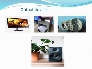
- 25. Output Device The output devices are used for delivering the results of computations to the outside world; examples are light emitting diodes, cathode ray tube (CRT) displays, digital-to-analog converters, card and paper-tape punches, character printers, plotters, communication lines etc.
- 26. Output devices
- 27. EXAMPLE OF A MICROCOMPUTER SYSTEM On the basis of the discussion in the previous sections, we can expand the microcomputer system shown in Figure 1 to include additional details. Figure 12 illustrates such a system. It shows the 8085 MPU, two types of memory (EPROM and R/WM), input and output, and the buses linking all peripherals (memory and I/Os) to the MPU.
- 28. References https://www.youtube.com/watch?v=oNKqRPv8c9M https://www.youtube.com/watch?v=eG3Vg_EZTYk https://www.slideshare.net/Johnrebel999/microcontroller-8051- 22899728 https://www.youtube.com/watch?v=te5Xe3TgPC4(addition of two numbers with animation) https://what-when-how.com/8051-microcontroller/assembling-and-running- an-8051-program/
- 29. Siddartha Institute of Science and Technology (Autonomous) (Approved by AICTE, New Delhi & Affiliated to JNTUA, Anantapuramu) (NAAC Accredited Institution with ‘A’ Grade) SIDDHARTH NAGAR, NARAYANAVANAM ROAD, PUTTUR – 517 583 CHITTOOR DIST., A.P., INDIA Department of Electronics & Communication Engineering UNIT-II 8085 Microprocessor Architecture SUBJECT:MICROPROCESSORS ANDMICROCONTROLLERS Academic Year-2022-23 Year/Semester-III/I HDr. Savitesh M. Sharma Mr Thyagarajan Prasad
- 30. COURSE OBJECTIVES Theobjectivesofthiscourse: 1. To understand the basic architecture of computer, evolution, and its applications 2. To learn the architectures of Microprocessor and Microcontroller 3. To learn the programming of Microprocessors and Microcontrollers using their programming model 4. To learn the interfacing of memory, I/O, sensors and actuators to microprocessors and microcontrollers
- 31. COURSE OUTCOMES On successful completion of this course, the student will be able 1. Understand the evolution of computers, processors, and its applications 2. Explain the various software and hardware parts of a microprocessors and computer 3. Understand the architectures of 8085,8086 microprocessors and 8051 microcontroller system 4. Analyze the programming model of 8085,8086 Microprocessors & 8051 microcontroller development environment. 5. Implement the techniques of interfacing memories, various I/O devices, sensors and actuators with microprocessor and microcontrollers 6. Design and develop various microprocessor/microcontroller- based systems for the real-life problems
- 32. Content ➢8085 Microprocessor Architecture: ❑The 8085 MPU - The 8085 Microprocessor, Microprocessor communication and bus timings, Demultiplexing the bus AD7-AD0, ❑Generating control signals ❑A detailed look at the 8085 MPU and its architecture– Instruction ❑Data format and Data Storage ❑Overview of the 8085 Instruction set .
- 33. 8085 MPU Microprocessor is a Central Processing Unit (CPU) etched on a single chip. A single Integrated Circuit (IC) has all the functional components of a CPU namely Arithmetic Logic Unit (ALU), Control Unit and registers. The 8085 microprocessor is an 8-bit processor that includes on its chip most of the logic circuitry for performing computing tasks and for communicating with peripherals.
- 34. 8085 microprocessor 8 bit microprocessor(8085 microprocessor can read or write or perform arithmetic and logical operations on 8-bit data at time) It has 8 data lines and 16 address lines hence capacity is 216 = 64 kB of memory Cock frequency is 3 MHz It requires +5V power supply. It is a single chip NMOS device implemented with 6200 transistors. It provides 74 instructions with five addressing modes. It provides 5 hardware interrupt and 8 software interrupts.
- 35. 8085 PIN DIAGRAM All the signals can be classified into six groups: (1) address bus, (2) data bus, (3) control and status signals, (4) power supply and frequency signals. (5) externally initiated signals, and (6) serial I/O ports ADDRESS BUS: The 8085 has 16 signal lines (pins) that are used as the address bus; however, these lines are split into two segments: A15-A8, and AD7-AD,0 The eight signal lines, A15-A8, a unidirectional and used for the most significant bits, called the high-order address of a 16-bit address. The signal lines AD7-AD0, are used for a dual purpose, as explained in the next section MULTIPLEXED ADDRESS/DATA BUS: The signal lines AD7-AD0, are bidirectional: they serve a dual purpose. They are used as the loworder address bus as well as the data bus. In executing an instruction, during the earlier part of the cycle, these lines are used as the low-order address bus.
- 36. PIN DIAGRAM
- 37. SIGNALS This group of signals includes two control signals (RD’ and WR’), three status signals (1O/M’, S1. and S0 to identify the nature of the operation, and one special signal (ALE) to indicate the beginning of the operation. These signals are as follows: 1) ALE-Address Latch Enable: This is a positive going pulse generated every time the 8085 begins an operation (machine cycle); it indicates that the bits on AD7-AD0, are address bits. This signal is used primarily to latch the low- order address from the multiplexed bus and generate a separate set of eight address lines, A7-A0. 2) RD’-Read: This is a Read control signal (active low). This signal indicates that the selected 1/O or memory device is to be read and data are available on the data bus. 3) WR’-Write: This is a Write control signal (active low). This signal indicates that the data on the data bus are to be written into a selected memory or I/O location. 4) IO/M’: This is a status signal used to differentiate between I/O and memory operations. When it is high, it indicates an I/O operation; when it is low, it indicates a memory operation. This signal is combined with RD’ (Read) and WR’ (Write) to generate I/O and memory control signals
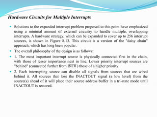
- 38. EXTERNALLY INITIATED SIGNALS, INCLUDING INTERRUPTS The 8085 has five interrupt signals that can be used to interrupt a program execution. One of the signals. INTR (Interrupt Request), is identical to the 8080A microprocessor interrupt signal (INT); the others are enhancements to the 8080A. The microprocessor acknowledges an interrupt request by the INTA (Interrupt Acknowledge) signal. In addition to the interrupts, three pins-RESET. HOLD, and READY-accept the externally initiated signals as inputs. To respond to the HOLD request, the 8085 has one signal called HLDA (Hold Acknowledge). RESET IN: When the signal on this pin goes low, the program counter is set to zero, the buses are tristated, and the MPU is reset. RESET OUT: This signal indicates that the MPU is being reset. The signal can be used to reset other devices. 8085 Interrupts and Externally initiated Signals INTR (Input); Interrupt Request: This is used as a general-purpose interrupt. it is similar to the INT signal of the 8080A. INTA’ (Output) :Interrupt Acknowledge: This is used to acknowledge an interrupt. RST 7.5 (Inputs)RST6.5, RST5.5 : Restart Interrupts: These are vectored interrupts that transfer the program control to specific memory locations. They have higher priorities than the INTR interrupt. Among these three, the priority order is 7.5. 6.5, and 5.5. HOLD (Input): This signal indicates that a peripheral such as a DMA (Direct Memory Access) controller is requesting the use of the address and data buses. HLDA (Output): Hold Acknowledge: This signal acknowledges the HOLD request. READY (Input): This signal is used to delay the microprocessor Read or Write cycles until a slow responding peripheral is ready to send or accept data. When this signal goes low, the microprocessor waits for an integral number of clock cycles until it goes high.
- 39. MICROPROCESSOR COMMUNICATION AND BUS TIMING 1. A courier gets the address from the office; he or she drives the pickup van, finds the street, and looks for your house number. 2. The courier rings the bell. 3. Somebody in the house opens the door and gives the package to the courier, and the courier returns to the office with the package. 4. The internal office staff disposes the package according to the instructions given by the customer Now let us examine the steps in the following example of how the microprocessor fetches or gets a machine code from memory.
- 40. Data Flow from Memory to the MPU
- 41. Timing: transfer byte from memory to MPU
- 42. DEMULTIPLEXING THE BUS AD7-AD0
- 43. Schematic to Generate Read/Write Control Signals for meory and I/O There are four different control signals are generated by combining the signals RD’, WR’, and IO/M’. The signal IO/M’ goes low for the memory operation. This signal is ANDed with RD and WR signals by using the 74LS32 quadruple two-input OR gates, as shown in Figure The OR gates are functionally connected as negative NAND gates. When both input signals go low, the outputs of the gates go low and generate MEMR’ (Memory Read) and MEMW’ (Memory Write) control signals. When the IO/M’ signal goes high, it indicates the peripheral I/O operation. Figure 5 shows that this signal is complemented using the Hex inverter 74LS04 and ANDed with the RD’ and WR’ signals to generate IOR (I/O Read) and IOW (I/O Write) control signals.
- 44. The 8085A Microprocessor: Functional Block Diagram
- 45. TIMING AND CONTROL UNIT This unit synchronizes all the microprocessor operations with the clock and generates the control signals necessary for communication between the microprocessor and peripherals. The control signals are similar to a sync pulse in an oscilloscope. The RD’ and WR’ signals are sync pulses indicating the availability of data on the data bus. INSTRUCTION REGISTER AND DECODER The instruction register and the decoder are part of the ALU. When an instruction is fetched from memory, it is loaded in the instruction register. The decoder decodes the instruction and establishes the sequence of events to follow. The instruction register is not programmable and cannot be accessed through any instruction REGISTER ARRAY The programmable registers are used to store the data temporarily. Two additional registers, called temporary registers W and Z, are included in the register array. These registers are used to hold 8-bit data during the execution of some instructions. However, because they are used internally, they are not available to the programmer. Decoding and Executing an Instruction Decoding and executing an instruction after it has been fetched can be illustrated with the example Example: Assume that the accumulator contains data byte 82H, and the instruction MOV C, A (4FH) is List the steps in decoding and executing the instruction. To decode and execute the instruction, the following steps are performed
- 47. Data Format of 8085 Microprocessor: The operand is an another name for data. It may appear in different forms : Addresses Numbers/Logical data and Characters Addresses : The address is a 16-bit unsigned integer ,number used to refer a memory location. Numbers/Data : The 8085 supports following numeric data types. • Signed Integer : A signed integer number is either a positive number or a negative number. In 8085, 8-bits are assigned for signed integer, in which most significant bit is used for sign and remaining seven bits are used for Sign bit 0 indicates positive number whereas sign bit 1 indicates negative number. • Unsigned Integer : The 8085 microprocessor supports 8-bit unsigned integer. • BCD : The term BCD number stands for binary coded decimal number. It uses ten digits from 0 through 9. The 8-bit register of 8085 can store two digit BCD Characters : The 8085 uses ASCII code to represent characters. It is a 7-bit alphanumeric code that represents decimal numbers, English alphabets, and other special characters.
- 48. DATA STORAGE: For storing data and Instructions Data storage known as memory are used with microprocessor. Memory is a storage of binary bits. Memory chips used in most systems are 8-bit registers stacked one above the other. It includes four registers and each register can store 8 bits. This chip can be referred to as a 4-byte or 32 bit (4X8 ) bits memory chip. It has two address lines A0 and A1 to identify four registers, 8 data lines to store 8 bits and three timing control signals: Read (RD’), Write (WR’) and Chip select (CS’): all control signals are designed to be active low. The processor can select this chip and identify its register and store (write) or access (read) 8 bit at a time.The memory addresses assigned to these registers are determined by the interfacing logic used in the system.
- 49. OVERVIEW OF THE 8085 INSTRUCTION SET The 8085 microprocessor instruction set has 74 operation codes that result in 246 in- structions. The set includes all the 8080A instructions plus two additional instructions (SIM and RIM, related to serial I/O). It is an overwhelming experience for a beginner to study these instructions. You are strongly advised not to attempt to read all these instructions at one time. However, you should be able to grasp an overview of the set by examining the frequently used instructions listed below The following notations are used in the description of the instructions
- 50. Data Transfer (Copy) Instructions: These instructions perform the following six operations. (i) Load an 8-bit number in a register (ii) Copy from register to register (iii) Copy between I/O and accumulator (iv) Load 16-bit number in a register pair (v) Copy between register and memory (vi) Copy between registers and stack memory
- 51. Summary – Data transfer MOV Move MVI Move Immediate LDA Load Accumulator Directly from Memory STA Store Accumulator Directly in Memory LHLD Load H & L Registers Directly from Memory SHLD Store H & L Registers Directly in Memory 8085 Instruction Set 51
- 52. Summary Data transfer An 'X' in the name of a data transfer instruction implies that it deals with a register pair (16-bits); LXI Load Register Pair with Immediate data LDAX Load Accumulator from Address in Register Pair STAX Store Accumulator in Address in Register Pair XCHG Exchange H & L with D & E XTHL Exchange Top of Stack with H & L 8085 Instruction Set 52
- 53. Summary - Arithmetic Group Add, Subtract, Increment / Decrement data in registers or memory. ADD Add to Accumulator ADI Add Immediate Data to Accumulator ADC Add to Accumulator Using Carry Flag ACI Add Immediate data to Accumulator Using Carry SUB Subtract from Accumulator SUI Subtract Immediate Data from Accumulator SBB Subtract from Accumulator Using Borrow (Carry) Flag SBI Subtract Immediate from Accumulator Using Borrow (Carry) Flag INR Increment Specified Byte by One DCR Decrement Specified Byte by One INX Increment Register Pair by One DCX Decrement Register Pair by One DAD Double Register Add; Add Content of Register Pair to H & L Register Pair 8085 Instruction Set 53
- 54. Summary Logical Group This group performs logical (Boolean) operations on data in registers and memory and on condition flags. These instructions enable you to set specific bits in the accumulator ON or OFF. ANA Logical AND with Accumulator ANI Logical AND with Accumulator Using Immediate Data ORA Logical OR with Accumulator OR Logical OR with Accumulator Using Immediate Data XRA Exclusive Logical OR with Accumulator XRI Exclusive OR Using Immediate Data 8085 Instruction Set 54
- 55. The Compare instructions compare the content of an 8-bit value with the contents of the accumulator; CMP Compare CPI Compare Using Immediate Data The rotate instructions shift the contents of the accumulator one bit position to the left or right: RLC Rotate Accumulator Left RRC Rotate Accumulator Right RAL Rotate Left Through Carry RAR Rotate Right Through Carry Complement and carry flag instructions: CMA Complement Accumulator CMC Complement Carry Flag STC Set Carry Flag 8085 Instruction Set 55
- 56. Summary - Branch Group Unconditional branching JMP Jump CALL Call RET Return Conditions NZ Not Zero (Z = 0) Z Zero (Z = 1) NC No Carry (C = 0) C Carry (C = 1) PO Parity Odd (P = 0) PE Parity Even (P = 1) P Plus (S = 0) M Minus (S = 1) Conditional branching 8085 Instruction Set 56 Summary -Machine control instruction HLT Stop processing and wait NOP Do not perform any operation
- 57. TEXT BOOKS 1. Ramesh Gaonkar, Microprocessor Architecture, programming and applications with the 8085, Penram International Publications Pvt Ltd. 6th Edition, 2015. 2. Kenneth J Ayala, The 8051 microcontroller, Penram International Publications Pvt Ltd, 2 nd Edition, 1997 REFERENCES 1. Ray Bhurchandi, Advanced Microprocessors & Peripheral interfacing, MC graw hill Publications, 3 rd edition, 2012. 2. N.Senthil Kumar, M.Saravanan, S.Jeevanathan, Microprocessor and Microcontrollers, Oxford Publishers. 1 st Edition, 2015. References
- 59. Siddartha Institute of Science and Technology (Autonomous) (Approved by AICTE, New Delhi & Affiliated to JNTUA, Anantapuramu) (NAAC Accredited Institution with ‘A’ Grade) SIDDHARTH NAGAR, NARAYANAVANAM ROAD, PUTTUR – 517 583 CHITTOOR DIST., A.P., INDIA Department of Electronics & Communication Engineering UNIT -III The 8051 Microcontroller Architecture SUBJECT:MICROPROCESSORSAND MICROCONTROLLERS Academic Year-2022-23 Year/Semester-III/I HDr. Savitesh M. Sharma Mr Thyagarajan Prasad
- 60. COURSE OBJECTIVES The objectivesof thiscourse: 1. To understand the basic architecture of computer, evolution, and its applications 2. To learn the architectures of Microprocessor and Microcontroller 3. To learn the programming of Microprocessors and Microcontrollers using their programming model 4. To learn the interfacing of memory, I/O, sensors and actuators to microprocessors and microcontrollers
- 61. COURSE OUTCOMES On successful completion of this course, the student will be able 1. Understand the evolution of computers, processors, and its applications 2. Explain the various software and hardware parts of a microprocessors and computer 3. Understand the architectures of 8085,8086 microprocessors and 8051 microcontroller system 4. Analyze the programming model of 8085,8086 Microprocessors & 8051 microcontroller development environment. 5. Implement the techniques of interfacing memories, various I/O devices, sensors and actuators with microprocessor and microcontrollers 6. Design and develop various microprocessor/microcontroller- based systems for the real-life problems
- 62. Content ➢The 8051 Architecture: ❑ Introduction ❑8051 microcontroller hardware ❑Input/output pins ❑ports and circuits ❑External memory ❑Counters and timers ❑ Serial data input/output ❑Interrupts
- 64. ALL OF THE FEATURES UNIQUE TO MICROCONTROLLERS 8051 Internal ROM and RAM I/O ports with programmable pins Timers and counters Serial data communication The figure also shows the usual CPU components: program counter, ALU, working registers, and clock circuits. The 8051 architecture consists of these specific features: Eight-bit CPU with registers A (the accumulator) and B Sixteen-bit program counter (PC) and data pointer (DPTR) Eight-bit program status word (PSW) Eight-bit stack pointer (SP) Internal ROM or EPROM (8751) of 0 (8031) to 4K (8051) Internal RAM of 128 bytes: Four register banks, each containing eight registers Sixteen bytes, which may be addressed at the bit level Eighty bytes of general-purpose data memory Thirty-two input/output pins arranged as four 8-bit ports: PO-P3 Two 16-bit timer/counters: TO and TI Full duplex serial data receiver/transmitter: SBUF Control registers: TCON, TMOD, SCON, PCON, IP, and IE Two external and three internal interrupt sources
- 65. PIN DIAGRAM OF 8051 A pinout of the 8051 packaged in a 40-pin DIP is shown in Figure show with the full and abbreviated names of the signals for each pin. It is important to note that many of the pins are used for more than one function (the alternate functions are shown in parentheses in Figure 2). Not all of the possible 8051 features may be used at the same time
- 66. The 8051 Oscillator and Clock The heart of the 8051 is the circuitry that generates the clock pulses by which all internal operations are synchronized. Pins XTALI and XTAL2 are provided for connecting a resonant network to form an oscillator. Typically, a quartz crystal and capacitors are employed, as shown in Figure 3. The crystal frequency is the basic internal clock frequency of the microcontroller. The manufacturers make available 8051 designs that can run at specified maximum and minimum frequencies, typically I megahertz to 16 megahertz. Minimum frequencies imply that some internal memories are dynamic and must always operate above a minimum frequency, or data will be lost
- 67. PROGRAM COUNTER AND DATA POINTER The 8051 contains two 16-bit registers: the program counter (PC) and the data pointer (DPTR). Each is used to hold the address of a byte in memory. Program instruction bytes are fetched from locations in memory that are addressed by the PC. Program ROM may be on the chip at addresses 0000h to OFFFh, external to the chip for addresses that exceed 0FFFh, or totally external for all addresses from 0000h to FFFFh. The PC is automatically incremented after every instruction byte is fetched and may also be altered by certain instructions. The PC is the only register that does not have an internal address
- 68. Flags and the Program Status Word (PSW) Flags are 1-bit registers provided to store the results of certain program instructions. Other instructions can test the condition of the flags and make decisions based upon the flag states. In order that the flags may be conveniently addressed, they are grouped inside the program status word (PSW) and the power control (PCON) registers.
- 69. INTERNAL MEMORY A functioning computer must have memory for program code bytes, commonly in ROM, and RAM memory for variable data that can be altered as the program runs. The 8051 has internal RAM and ROM memory for these functions. Additional memory can be added externally using suitable circuits. INTERNAL RAM The 128-byte internal RAM, which is shown generally in Figure 1 and in detail in Figure 5, is organized into three distinct areas: 1. Thirty-two bytes from address 00h to 1 Fh that make up 32 working registers organized as four banks of eight registers each. The four register banks are numbered 0 to 3 and are made up of eight registers named R0 to R 7. Each register can be addressed by name (when its bank is selected) or by its RAM address. Thus R0 of bank 3 is R0 (if bank 3 is currently selected) or address 18h (whether bank 3 is selected or not). Bits RS0 and RS 1 in the PSW determine which bank of registers is currently in use at any time when the program is running. Register banks not selected can be used as general-purpose RAM. Bank 0 is selected upon reset.
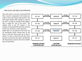
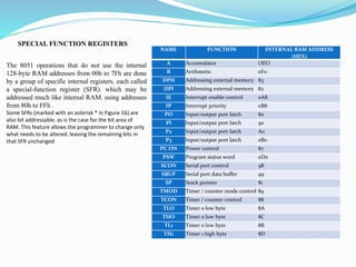
- 70. THE STACK AND THE STACK POINTER The stack refers to an area of internal RAM that is used in conjunction with certain op- codes to store and retrieve data quickly. The 8-bit stack pointer (SP) register is used by the 8051 to hold an internal RAM address that is called the "top of the stack." The address held in the SP register is the location in internal RAM where the last byte of data was stored by a stack operation. When data is to be placed on the stack, the SP increments before storing data on the stack so that the stack grows up as data is stored. As data is retrieved from the stack, the byte is read from the stack, and then the SP decrements to point to the next available byte of stored data.
- 71. SPECIAL FUNCTION REGISTERS NAME FUNCTION INTERNAL RAM ADDRESS (HEX) A Accumulator OEO B Arithmetic 0F0 DPH Addressing external memory 83 DPl Addressing external memory 82 IE Interrupt enable control 0A8 IP Interrupt priority 0B8 PO Input/output port latch 80 Pl Input/output port latch 90 P2 Input/output port latch A0 P3 Input/output port latch 0B0 PC ON Power control 87 PSW Program status word 0D0 SCON Serial port control 98 SBUF Serial port data buffer 99 SP Stack pointer 81 TMOD Timer / counter mode control 89 TCON Timer / counter control 88 TLO Timer 0 low byte 8A THO Timer 0 low byte 8C TL1 Timer 0 low byte 8B TH1 Timer 1 high byte 8D The 8051 operations that do not use the internal 128-byte RAM addresses from 00h to 7Fh are done by a group of specific internal registers. each called a special-function register (SFR). which may be addressed much like internal RAM. using addresses from 80h to FFh . Some SFRs (marked with an asterisk * in Figure 1b) are also bit addressable. as is the case for the bit area of RAM. This feature allows the programmer to change only what needs to be altered. leaving the remaining bits in that SFR unchanged
- 72. INPUT/OUTPUT PINS, PORT AND CIRCUITS I/O ports of 8051: There are four ports P0, P1, P2 and P3 each use 8 pins, making them 8-bit ports. All the ports upon RESET are configured as output, ready to be used as output ports. To use any of these ports as an input port, it must be programmed. Each port of 8051 has bidirectional capability. Port 0 is called 'true bidirectional port' as it floats (tristated) when configured as input. Port-1, 2, 3 are called 'quasi bidirectional port'. Configuration : • The below figures represent one bit (one line) of Port 0, 1,2 & 3. • Every port line has a one-bit latch, in the form of a D Flip Flop • It is used to hold the value on the port, when used as an output port. • The latch will capture a “0” or a “1” from the internal bus, on getting “write to latch” signal. • The port also has buffers that allow us to either read from the latch or read from the port line. Input operation: • When a “1” is written to the latch, the port becomes an input port, by turning the FETs off. Output operation: • To send a “0”: Write a “0” on the latch. This turns ON the FET and the port pin gets grounded, so the port pin contains logic “0”. • To send a “1”: Write a “1” on the latch. This turns OFF the FET and the port line “floats”, containing neither logic 0 nor1 (just like input). • By connecting VCC using an external pull up resister, we can output a “1” on the port line. Alternate function: • Port 0 can also be used as the multiplexed bus AD7 – AD0, and can carry address or data. • Port 1 does not have alternate functions. • Port 2 can be used as the higher order address bus (A15 – A8). • The “control” signal shown in the Port 0, Port 2 diagrams directs the address line to the “gate” of the FET. • Port 3 can be used as (P3.0-RXD, P3.1-TXD, P3.2-INT0, P3.3-INT1,P3.4- T0, P3.5 – T1, P3.6 – WR, P3.7 – RD). The “Alternate Output function” signal directs the alternate function to the “gate” of the FET
- 73. PORT 0 PIN CONGIGURATION PORT 1 PIN CONGIGURATION
- 74. PORT 2 PIN CONGIGURATION PORT 3 PIN CONGIGURATION
- 75. EXTERNAL MEMORY The system designer is not limited by the amount of internal RAM and ROM available on chip. Two separate external memory spaces are made available by the 16-bit PC and DPTR and by different control pins for enabling external ROM and RAM chips. Internal control circuitry accesses the correct physical memory, depending upon the machine cycle state and the op code being executed. There are several reasons for adding external memory, particularly program memory, when applying the 8051 in a system. When the project is in the prototype stage, the expense—in time and money—of having a masked internal ROM made for each program "try" is prohibitive.
- 77. COUNTER AND TIMERS it is a device that counts down from a specified time interval and used to generate a time delay, for example, an hourglass is a timer. a counter is a device that stores (and sometimes displays) the number of times a particular event or process occurred, with respect to a clock signal. FIGURE TIMER/COUNTER LOGIC TIMER COUNTER INTERRUPTS It is a device that counts down from a specified time interval and used to generate a time delay, for example, an hourglass is a timer. A counter is a device that stores (and sometimes displays) the number of times a particular event or process occurred, with respect to a clock signal. For example, an interrupt occurs when a down counting timer reaches 0 and reloads the modulus in the main counter. The timer sends a hardware signal to an “interrupt controller” which suspends execution of the main program and makes the processor jump to a software function called an “interrupt service routine” or ISR
- 78. TIMER MODES OF OPERATION Timers of 8051:• 8051 has 2, 16-bit Up Counters T1 and T0. • If the counter counts internal clock pulses it is known as timer. • If it counts external clock pulses it is known as counter. • Each counter is divided into 2, 8-bit registers TH1 - TL1 and TH0 - TL0. • The timer action is controlled mainly by the TCON and the TMOD registers. TCON - Timer Control (SFR) [Bit-Addressable As TCON.7 to TCON.0] TF1 and TF0: (Timer Overflow Flag) • Set (1) when Timer 1 or Timer 0 overflows respectively i.e. its bits roll over from all 1's to all 0's. • Cleared (0) when the processor executes ISR (address 001BH for Timer 1 and 000BH for Timer 0). TR1 and TR0: (Timer Run Control Bit) • Set (1) - Starts counting on Timer 1 or Timer 0 respectively. • Cleared (0) - Halts Timer 1 or Timer 0 respectively. IE1 and IE0: (External Interrupt Edge Flag) Set (1) when external interrupt signal received at INT1 or INT0 respectively. Cleared (0) when ISR executed (address 0013H for Timer 1 and 0003H for Timer 0) IT1 and IT0: (External Interrupt Type Control Bit) • Set (1) - Interrupt at INT1 or INT0 must be -ve edge triggered. Cleared (0) - Interrupt at INT1 or INT0 must be low-level triggered.
- 79. TMOD - Timer Mode Control (SFR) [NOT Bit-Addressable] C/T: (Counter/Timer) •Set (1) - Acts as Counter (Counts external frequency on T1 and T0 pin inputs). •Cleared (0) - Acts as Timer (Counts internal clock frequency, fosc/12). Gate: (Gate Enable Control bit) •Set (1) - Timer controlled by hardware i.e. INTX signal. •Cleared (0) – Counting independent of INTX signal. M1, M0: (Mode Selection bits) Used to select the operational
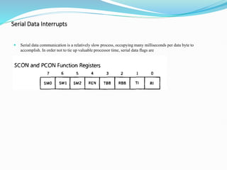
- 80. SERIAL DATA INPUT /OUTPUT Computers must be able to communicate with other computers in modern multiprocessor distributed systems. One cost-effective way to communicate is to send and receive data bits serially. The 8051 has a serial data communication circuit that uses register SBUF to hold data. Register SCON controls data communication, register PCON controls data rates, and pins RXD (P3.0) and TXD (P3.1) connect to the serial data network. SBUf is physically two registers. One is write only and is used to hold data to be transmitted out of the 8051 via TXD. The other is read only and holds received data from external sources via RXD. Both mutually exclusive registers use address 99h. There are four programmable modes for serial data communication that are chosen by setting the SMX bits in SCON. Baud rates are determined by the mode chosen. Figure 13 shows the bit assignments for SCON and PCON.
- 81. Serial Data Interrupts Serial data communication is a relatively slow process, occupying many milliseconds per data byte to accomplish. In order not to tie up valuable processor time, serial data flags are
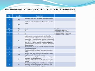
- 82. THE SERIAL PORT CONTROL (SCON) SPECIAL FUNCTION REGISTER Bit symbol Function 7 SM0 Serial port mode bit 0. Set/cleared by program to select mode. 6 SM1 Serial port mode bit 1. Set/cleared by program to select mode. SM0 SM1 Mode Description 0 0 0 Shift register; baud = f/12 0 1 1 8-bit UART; baud = variable 1 0 2 9-bit UART; baud = 1/32 or f/64 1 1 3 9-bit UART; baud = variable 5 SM2 Multiprocessor communications bit. Set/cleared by program to enable multiprocessor communications in modes 2 and 3. When set to 1 an interrupt is generated if bit 9 of the received data is a 1; no interrupt is generated if bit 9 is a 0. If set to 1 for mode 1, no interrupt will be generated unless a valid stop bit is received. Clear to 0 if mode 0 is in use. 4 REN Receive enable bit. Set to 1 to enable reception; cleared to 0 to disable reception. 3 TB8 Transmitted bit B. Set/cleared by program in modes 2 and 3. 2 RB8 Received bit B. Bit B of received data in modes 2 and 3; stop bit in mode 1. Not used in mode 0. 1 T1 Transmit interrupt flag. Set to one at the end of bit 7 time in mode 0, and at the beginning of the stop bit for other modes. Must be cleared by the program. 0 R1 Receive interrupt flag. Set to one at the end of bit 7 time in mode 0, and halfway through the stop bit for other modes. Must be cleared by the program.
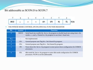
- 83. Bit addressable as SCON.O to SCON.7 THE POWER MODE CONTROL (PCON) SPECIAL FUNCTION REGISTER Bit symbol Function 7 SMOD Serial baud rate modify bit. Set to 1 by program to double baud rate using timer 1 for modes 1, 2, and 3. Cleared to 0 by program to use timer 1 baud rate. 6-4 - Not implemented. 3 GF1 General purpose user flag bit 1. Set/cleared by program. 2 GF0 General purpose user flag bit 0 . Set/cleared by program. 1 PD Power down bit. Set to 1 by program to enter power down configuration for CHMOS processors. 0 IDL Idle mode bit. Set to 1 by program to enter idle mode configuration for CHMOS processors. PCON is not bit addressable.
- 84. DATA TRANSMISSION Transmission of serial data bits begins anytime data is written to SBUF. T1 is set to a 1 when the data has been transmitted and signifies that SBUF is empty (for transmission purposes) and that another data byte can be sent. If the program fails to wait for the T1 flag and overwrites SBUF while a previous data byte is in the process of being transmitted, the results will be unpredictable (a polite term for "garbage out"). DATA RECEPTION Reception of serial data will begin if the receive enable bit (REN) in SCON is set to 1 for all modes. In addition, for mode 0 only, R1 must be cleared to 0 also. Receiver interrupt flag R1 is set after data has been received in all modes. Setting REN is the only direct program control that limits the reception of unexpected data; the requirement that R1 also be 0 for mode 0 prevents the reception of new data until the program has dealt with the old data and reset R1. SERIAL DATA TRANSMISSION MODES The 8051 designers have included four modes of serial data transmission that enable data communication to be done in a variety of ways and a multitude of baud rates. Modes are selected by the programmer by setting the mode bits SM0 and SM1 in SCON. Baud rates are fixed for mode 0 and variable, using timer 1 and the serial baud rate modify bit (SMOD) in PCON, for modes 1. 2. and 3.
- 85. SERIAL DATA MODE 0-SHIFT REGISTER MODE Setting bits SM0 and SM 1 in SCON to 00b configures SBUF to receive or transmit eight data bits using pin RXD for both functions. Pin TXD is connected to the internal shift frequency pulse source to supply shift pulses to external circuits. The shift frequency, or baud rate, is fixed at 1/12 of the oscillator frequency, the same rate used by the timers when in the timer configuration. The TXD shift clock is a square wave that is low for machine cycle states S3-S4-S5 and high for S6-S1-S2. Figure 14 shows the timing for mode 0 shift register data transmission.
- 86. INTERRUPTS Interrupts are the events that temporarily suspend the main program, pass the control to other functions or sources and execute their task. It then passes the control to the main program where it had left off. As code size increases and your application handles multiple modules, sequential coding would be too long and too complex. The interrupt mechanism helps to embed your software with hardware in a much simpler and efficient manner. In this topic, we will discuss the interrupts in 8051 using AT89S52 microcontroller. TIMER FLAG INTERRUPTS Each Timer is associated with a Timer interrupt. When a timer has finished counting, the Timer interrupt will notify the microcontroller by setting the required flag bit SERIAL PORT INTERRUPT This interrupt is used for serial communication. When enabled, it notifies the controller when a byte has been received or transmitted according to how the interrupt is configured. EXTERNAL INTERRUPTS 8051 based AT89S52 microcontroller has two active-low external interrupts, INT0 and INT1. See more information here: EXTERNAL INTERRUPT IN 8051 MICROCONTROLLER.
- 87. IE register (Interrupt Enable Register) EA bit enables or disables all interrupt sources (globally): • 0 – disables all interrupts (even enabled). 1 – enables specific interrupts. EX0 bit enables or disables External interrupt 0: • 0 – External interrupt 0 disabled.1 – External interrupt 0 enabled. ET0 bit enables or disables Timer T0 interrupt: • 0 – Timer T0 interrupt disabled. 1 – Timer T0 interrupt enabled. EX1 bit enables or disables External interrupt 1: • 0 – External interrupt 1 disabled. 1 – External interrupt 1 enabled. ET1 bit enables or disables Timer 1 overflow interrupt: • 0 – Timer 1 overflow interrupt disabled. 1 – Timer 1 overflow interrupt enabled. ES bit enables or disables serial port interrupt : • 0 – serial port interrupt disabled. 1 – serial port interrupt enabled. ET2 bit enables or disables Timer 2 overflow interrupt : • 0 – Timer 2 overflow interrupt disabled. 1 – Timer 2 overflow interrupt enabled.
- 88. IP Register (Interrupt Priority Register) • PT2: It defines the Timer 2 interrupt priority level (8052 only). • PS: It defines the serial port interrupt priority level. • PT1: It defines the Timer 1 interrupt priority level. • PX1: It defines the external interrupt priority level. • PT0: It defines the Timer 0 interrupt priority level. • PX0: It defines the external interrupt 0 priority level. Interrupt Subroutine ( ISR ) Once all the configurations are done, the next step is to write the functions to execute when an interrupt occurs. And this is done by writing ISR functions. This function gets called automatically when an interrupt occurs.
- 89. RESET A reset can be considered to be the ultimate interrupts because the program may not block the action of the voltage on the RST pin, this type of interrupt is often called non maskable ,because no combination of bit in any register can stop or mask the reset action .unlike other interrupts the PC is not stored for later program resumption . INTERRUPT CONTROL The program must be able at critical times to inhibit the action of some or all of the interrupts so that crucial operational can be finished. the IE register hold s the programmable bit that can enable or disable all the interrupts as a group or if the group is enabled each individual interrupt source can be enabled or disabled INTERRUPT ENABLE/DISABLE Bits in the IE register are set to 1 if the corresponding interrupt source is to be enabled and set to 0 to disable the interrupt source. bit EA is a master or global bit that can enable or disable all of the interrupts
- 90. INTERRUPT PRIORITY Register IP bits determine if any interrupt is to have a hight or low priority, bits set to 1 give the accompanying interrupt a high priority a 0 assigns a low priority. 0 assigns low priority. IE0 TF0 1E1 TF1 SERIAL=RI OR TI INTERRUPT DESTINATIONS each interrupt source causes the program to do a hardware call to one of the dedicated addresses in program memory it is the responsibility of the program to place a routine at the address that will service the interrupt.
- 91. TEXT BOOKS 1. Ramesh Gaonkar, Microprocessor Architecture, programming and applications with the 8085, Penram International Publications Pvt Ltd. 6th Edition, 2015. 2.Kenneth J Ayala, The 8051 microcontroller, Penram International Publications Pvt Ltd, 2 nd Edition, 1997 REFERENCES 1. Ray Bhurchandi, Advanced Microprocessors & Peripheral interfacing, MC graw hill Publications, 3 rd edition, 2012. 2. N.Senthil Kumar, M.Saravanan, S.Jeevanathan, Microprocessor and Microcontrollers, Oxford Publishers. 1 st Edition, 2015. References
- 93. Siddartha Institute of Science and Technology (Autonomous) (Approved by AICTE, New Delhi & Affiliated to JNTUA, Anantapuramu) (NAAC Accredited Institution with ‘A’ Grade) SIDDHARTH NAGAR, NARAYANAVANAM ROAD, PUTTUR – 517 583 CHITTOOR DIST., A.P., INDIA Department of Electronics & Communication Engineering UNIT -1V PROGRAMMINGTHE 8051 SUBJECT:MICROPROCESSORSAND MICROCONTROLLERS Academic Year-2022-23 Year/Semester-III/I HDr. Savitesh M. Sharma Mr Thyagarajan Prasad
- 94. COURSE OBJECTIVES The objectivesof thiscourse: 1. To understand the basic architecture of computer, evolution, and its applications 2. To learn the architectures of Microprocessor and Microcontroller 3. To learn the programming of Microprocessors and Microcontrollers using their programming model 4. To learn the interfacing of memory, I/O, sensors and actuators to microprocessors and microcontrollers
- 95. COURSE OUTCOMES On successful completion of this course, the student will be able 1. Understand the evolution of computers, processors, and its applications 2. Explain the various software and hardware parts of a microprocessors and computer 3. Understand the architectures of 8085,8086 microprocessors and 8051 microcontroller system 4. Analyze the programming model of 8085,8086 Microprocessors & 8051 microcontroller development environment. 5. Implement the techniques of interfacing memories, various I/O devices, sensors and actuators with microprocessor and microcontrollers 6. Design and develop various microprocessor/microcontroller- based systems for the real-life problems
- 96. Content ➢Programming with 8051: ✓Addressing modes ✓Moving data ✓Logical opearations ✓Airthmetic ✓Jump and call
- 97. ADDRESSING MODES Register Direct Indirect Immediate Indexed
- 98. Immediate addressing mode In this addressing mode, the data on which the operation is to be performed is mentioned in the instruction. Instead of specifying an address, the instruction specifies an operand along with the operation that is to be performed. The instruction is 2 bytes when there is 8-bit data and 4 bytes when there is 16-bit data. Examples of instructions that use immediate addressing mode are: • MVI B 05 – This instruction transfers the data, that is 05, to register B. • JMP address – This instruction moves the execution of the program to the specified address. • LXI H 3000 – This instruction transfers the data, that is, 3000, to the H-L pair register.
- 99. Register addressing mode In this addressing mode, the instruction mentions a register which stores some data. The operation specified by the instruction is performed in the register specified by it. The instruction can also specify two registers. The size of the instructions in register addressing mode is 1 byte. The instruction’s opcode includes both the register and the operation to be performed. Examples of instructions that use register addressing mode are: • ADD B – This instruction adds the data within register B with the data in the accumulator and stores the result in the accumulator. • INR B – This instruction increases the data stored in register B by 1. • MOVE B, D – This instruction moves the content of register D to register B. • PCHL – This instruction transfers the contents stored in the HL pair to the program counter.
- 100. Direct addressing mode In this addressing mode, the instruction specifies some address which stores the data. This memory location is mentioned in the instruction as an operand. The size of an instruction in the direct addressing mode is 3 bytes. However, input/output instructions in direct addressing mode are 2 bytes. Examples of instructions that use direct addressing mode are: • IN 35 – This instruction reads the data from a port. The address of the port is 35. • LHLD address – This instruction loads the data stored in the memory location specified by ‘address’ into the HL pair. LDA 2050 – This instruction stores the contents of the memory location 2050H into the accumulator STA 2050 – This instruction stores the contents of the accumulator in the memory location 2050H.
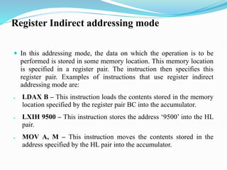
- 101. Register Indirect addressing mode In this addressing mode, the data on which the operation is to be performed is stored in some memory location. This memory location is specified in a register pair. The instruction then specifies this register pair. Examples of instructions that use register indirect addressing mode are: • LDAX B – This instruction loads the contents stored in the memory location specified by the register pair BC into the accumulator. • LXIH 9500 – This instruction stores the address ‘9500’ into the HL pair. • MOV A, M – This instruction moves the contents stored in the address specified by the HL pair into the accumulator.
- 102. Implied/Implicit addressing mode In this addressing mode, the operand is described implicitly in the definition of the instruction. The operand is specified with the opcode of the instruction. The size of an implied addressing mode instruction is 1 byte. The instructions generally operate on data stored in the accumulator. Examples of instructions that use implied addressing mode are as follows: • RRC – This instruction rotates the contents of the accumulator to the right by one bit. • RLC – This instruction rotates the contents of the accumulator to the left by one bit. • CMA – This instruction complements the content stored in the accumulator. The result is then stored in the accumulator itself.
- 103. EXTERNAL DATA MOVES It is possible to expand RAM and Rom memory space by adding external memory chips to the 8051 microcontroller the external memory can be as large as 64k for each of the RAM &ROM memory areas. opcodes that access this external memory always use indirect addressing to specify the external memory
- 104. Code memory read-only data moves Data moves between RAM locations and 8051 registers are made by using MOV and MOVX opcodes. The data is usually of a temporary or "scratch pad" nature and disappears when the system is powered down. There are times when access to a preprogrammed mass of data is needed, such as when using tables of predefined bytes. This data must be permanent to be of repeated use and is stored in the program ROM using assembler directives that store programmed data anywhere in ROM that the programmer wishes. Mnemonic Operation MOVC A,@A+DPTR Copy the code byte, found at the ROM address formed by adding A and the DPTR, to A MOVC A,@A+PC Copy the code byte, found at the ROM address formed by adding A and the PC, to A
- 105. PUSH AND POP OPCODE The PUSH and POP opcodes specify the direct address of the data. The data moves between an area of internal RAM, known as the stack, and the specified direct address. The stack pointer special-function register (SP) contains the address in RAM where data from the source address will be PUSHED, or where data to be POPED to the destination address is found. The SP register actually is used in the indirect addressing mode but is not named in the mnemonic. It is implied that the SP holds the indirect address whenever PUSHING or POPING. Figure 3.3 shows the operation of the stack pointer as data is PUSHED or POPED to the stack area in internal RAM. Mnemo nic Operation PUSH add Increment SP; copy the data in add to the internal RAM address contained in SP POP addCopy the data from the internal RAM address contained in SP to add; decrement the sp Mnemonic Operation MOV 81h,#30h Copy the immediate data 30h to the SP MOV R0, #0ACh Copy the immediate data ACh to R0 PUSH 00h SP = 31h; address 31h contains the number ACh PUSH 00h SP = 32h; address 32h contains the number ACh POP 0lh SP = 31 h; register R 1 now contains the number Ach POP 80h SP = 30h; port 0 latch now contains the number ACh
- 106. EXCHANGEOPCODES Exchanges between A and any port location copy the data on the port pins to A, while the data in A is copied to the port latch. Register A is used for so many instructions that the XCH opcode provides a very convenient way to "save" the contents of A without the necessity of using a PUSH opcode and then a POP opcode. Mnemonic Operation XCH A,Rr Exchange data bytes between register Rr and A XCH A,add Exchange data bytes between add and A XCH A,@Rp Exchange data bytes between A and address in Rp XCHD A,@Rp Exchange lower nibble between A and address in Rp Mnemonic Operation XCH A,R7 Exchange bytes between register A and register R7 XCH A,0F0h Exchange bytes between register A and register B XCH A,@R1 Exchange bytes between register A and address in R 1 XCHD A,@R1 Exchange lower nibble in A and the address in R 1
- 107. LOGICAL OPERATION BOOLEAN OPERATOR 8051 MNEMONIC AND ANL (AND logical) OR ORL (OR logical) XOR XRL (exclusive OR logical) NOT CPL (complement) The two data levels, byte or bit, at which the Boolean instructions operate are shown in the following table: Mnemonic Operation RL Rotate a byte to the left; the Most Significant Bit (MSB) becomes the Least Significant Bit (LSB) RLC Rotate a byte and the carry bit left; the carry becomes the LSB, the MSB becomes the carry RR Rotate a byte to the right; the LSB becomes the MSB RRC Rotate a byte and the carry to the right; the LSB becomes the carry, and the carry the MSB SWAP Exchange the low and high nibbles in a byte
- 108. Byte-Level Logical Operations The byte-level logical operations use all four addressing modes for the source of a data byte. The A register or a direct address in internal RAM is the destination of the logical operation result. Mnemonic Operation ANL A,#n AND each bit of A with the same bit of immediate number n; put the results in A ANL. A.add AND each bit of A with the same bit of the direct RAM address; put the results in A ANLA,Rr AND each bit of A with the same bit of register Rr; put the results in A AND each bit of A with the same bit of the contents of the RAM address contained in Rp; put the results in A ANL A,@Rp AND each bit of A with the direct RAM address; put the results in the direct RAM address ANL add.A AND each bit of the RAM address with the same bit in the number n; put the result in the RAM address ANL add,#n OR each bit of A with the same bit of n; put the results in A ORL A,#n OR each bit of A with the same bit of the direct RAM address; put the results in A ORL A,add OR each bit of A with the same bit of register Rr; put the results in A OR each bit of A with the same bit of the contents of the RAM address contained in Rp; put the results in A ORL A,Rr OR each bit of A with the direct RAM address; put the results in the direct RAM address ORL A,@Rp OR each bit of the RAM address with the same bit in the number n; put the result in the RAM address ORL add.A XOR each bit of A with the same bit of n; put the results in A ORL add,#n XOR each bit of A with the same bit of the direct RAM address; put the results in A XRL A,#n XOR each bit of A with the same bit of register Rr; put the results in A XOR each bit of A with the same bit of the contents of the RAM address contained in Rp; put the results in A XRL A,add XOR each bit of A with the direct RAM address; put the results in the direct RAM address XRL A,Rr Operation XRL A,@Rp AND each bit of A with the same bit of immediate number n; put the results in A XRL add.A AND each bit of A with the same bit of the direct RAM address; put the results in A XRL add,#n XOR each bit of the RAM address with the same bit in the number n; put the result in the RAM address CLRA Clear each bit of the A register to zero CPL A Complement each bit of A; every I becomes a 0, and each 0 becomes a 1
- 109. Bit-Level Logical Operations Certain internal RAM and SFRs can be addressed by their byte addresses or by the address of each bit within a byte. Bit addressing is very convenient when you wish to alter a single bit of a byte, in a control register for instance, without having to wonder what you need to do to avoid altering some other crucial bit of the same byte. The assembler can also equate bit addresses to labels that make the program more readable. For example, bit 4 of TCON can become TR0, a label for the timer 0 run bit.
- 110. Internal RAM Bit Addresses The availability of individual bit addresses in internal RAM makes the use of the RAM very efficient when storing bit information. Whole bytes do not have to be used up to store one or two bits of data. BYTE ADDRESS (HEX) BIT ADDRESSES (HEX) 20 00-07 21 08-0F 22 10-17 23 18-lF 24 20-27 25 28-2F 26 30-37 27 38-3F 28 40-47 29 48-4F 2A 50-57 28 58-5F 2C 60-67 20 68-6F 2E 70-77 2F 78-7F
- 111. SFR Bit Addresses All SFRs may be addressed at the byte level by using the direct address assigned to it, but not all of the SFRs are addressable at the bit level. The SFRs that are also bit addressable form the bit address by using the five most significant bits of the direct address for that SFR, together with the three least significant bits that identify the bit position from position 0 (LSB) to 7 (MSB). SFR DIRECT ADDRESS (HEX) BIT ADDRESSES (HEX) A OED OEO-OE7 6 OFO OFO-OF7 IE OAS OAS-OAF IP 06S 06S-06F PO so SO-S7 Pl 90 90-97 P2 OAO OAO-OA7 P3 060 060-067 PSW ODO ODO-OD7 TCON SS SS-SF SCON 9S 9S-9F
- 112. Bit-Level Boolean Operations The bit-level Boolean logical opcodes operate on any addressable RAM or SFR bit. The carry flag (C) in the PSW special-function register is the destination for most of the opcodes because the flag can be tested and the program flow changed using instructions covered The following table lists the Boolean bit-level operations. Mnemonic Operation ANL C,b AND C and the addressed bit; put the result in C ANL C,/b AND C and the complement of the addressed bit; put the result in C; the addressed bit is not altered ORL C,b OR C and the addressed bit; put the result in C ORLC,/b OR C and the complement of the addressed bit; put the result in C; the addressed bit is not altered CPLC Complement the C flag CPL b Complement the addressed bit CLRC Clear the C flag to zero CLR b Clear the addressed bit to zero MOV C,b Copy the addressed bit to the C flag MOV b,C Copy the C flag to the addressed bit SETB C Set the flag to one SETB b Set the addressed bit to one
- 113. Bit-Addressable Control Registers 7 6 5 4 3 2 1 0 CY AC F0 RSI RS0 0V Reserved P PROGRAM STATUS WORD (PSW) SPECIAL FUNCTION REGISTER. BIT ADDRESSES D0h to D7h. Bit Function 7 Carry flag 6 Auxiliary carry flag 5 User flag 0 4 Register bank select bit 1 3 Register bank select bit 0 2 Overflow flag 1 Not used (reserved for future) 0 Parity flag
- 114. INTERRUPT ENABLE (IE) SPECIAL FUNCTION REGISTER. BIT ADDRESSES A8h TO AFh. 7 6 5 4 3 2 1 0 EA Reserve d Reserve d ES ET1 EX 1 ET0 EX0 Bit Function 7 Disables all interrupts 6 Not used (reserved for future) 5 Not used (reserved for future) 4 Serial port interrupt enable 3 Timer 1 overflow interrupt enable 2 External interrupt 1 enable 1 Timer 0 interrupt enable 0 External interrupt 0 enable EA disables all interrupts when cleared to 0; if EA = 1 then each individual interrupt will be enabled if 1, and disabled if 0.
- 115. INTERRUPT PRIORITY (IP) SPECIAL FUNCTION REGISTER. BIT ADDRESSES B8h to BFh. 7 6 5 4 3 2 1 0 * * Reserved PS PT1 PX1 PT0 PX0 Bit Function 7 Not implemented 6 Not implemented 5 Not used (reserved for future) 4 Serial port interrupt priority 3 Timer 1 interrupt priority 2 External interrupt 1 priority 1 Timer 0 interrupt priority The priority bit may be set to 1 (highest) or 0 (lowest).
- 116. TIMER/COUNTER CONTROL (TCON) SPECIAL FUNCTION REGISTER. BIT ADDRESSES 88h to 8Fh 7 6 5 4 3 2 1 0 TF1 TR1 TF0 TR0 IE1 IT1 IE0 IT0 Bit Function 7 Timer 1 overflow flag 6 Timer run control 5 Timer 0 overflow flag 4 Timer 0 run control 3 External interrupt 1 edge flag 2 External interrupt 1 mode control 1 External interrupt 0 edge flag 0 External interrupt 0 mode control All flags can be set by the indicated hardware action; the flags are cleared when interrupt is serviced by the processor
- 117. SERIAL PORT CONTROL (SCON) SPECIAL FUNCTION REGISTER. BIT ADDRESSES 98h to 9Fh 7 6 5 4 3 2 1 0 SM0 SM1 SM2 REN TBB RBB TI RI Bit Function 7 Serial port mode bit 0 6 Serial port mode bit 1 5 Multiprocessor communications enable 4 Receive enable 3 Transmitted bit in modes 2 and 3 2 Received bit in modes 2 and 3 1 Transmit interrupt flag 0 Receive interrupt flag
- 118. Rotate and Swap Operations The ability to rotate data is useful for inspecting bits of a byte without using individual bit opcodes. The A register can be rotated one bit position to the left or right with or without including the C flag in the rotation. If the C flag is not included, then the rotation involves the eight bits of the A register. If the C flag is included, then nine bits are involved in the rotation. Including the C flag enables the programmer to construct rotate operations involving any number of bytes. Mnemonic Operation RL A Rotate the A register one bit position to the left; bit A0 to bit A I, A I to A2. A2 to A3. A3 to A4, A4 to A5, A5 to A6. A6 to A 7, and A 7 to A0 RLC A Rotate the A register and the carry flag. as a ninth bit, one bit position to the left; bit A0 to bit Al, Al to A2, A2 to A3, A3 to A4, A4 to A5. A5 to A6, A6 to A 7, A 7 to the carry flag, and the carry flag to A0 RR A Rotate the A register one bit position to the right; bit A0 to bit A 7, A6 to A5, A5 to A4, A4 to A3, A3 to A2. A2 to Al, and At to A0 RRC A Rotate the A register and the carry flag, as a ninth bit, one bit position to the right; bit A0 to the carry flag. carry flag to A 7, A 7 to A6, A6 to A5, A5 to A4, A4 to A3, A3 to A2, A2 to Al, and Al to A0 SWAP A Interchange the nibbles of register A; put the high nibble in the low nibble position and the low nibble in the high nibble position
- 119. Figure Register a rotate operation
- 120. The following table shows examples of rotate and swap operations: Mnemonic Operation OY A,#OA5h A = I0l00I0lb = A5h RR A A = I I0I00I0b = D2h RR A A = 0l I0l00lb = 69h RR A A = I0I l0I00b = B4h RR A A = 0I0l I0I0b = 5Ah SWAP A A= I0I00I0lb = A5h CLR C C = 0; A = I0I00I0lb = A5h RRC A C = I; A= 0I0I00I0b = 52h RRC A C = 0; A = l0I0J00lb = A9h RL A A= 0I0I00llb = 53h RL A A = I0I00l I0b = A6h SWAP A C = 0; A = 0l 101010b = 6Ah RLC A C = 0; A = 1 I0I0l00b = D4h RLC A C = l; A= I0I0l000b = A8h SWAP A C = l; A= l000I0I0b = 8Ah
- 121. ARITHMETIC OPERATIONS FLAGS a key part of performing arithmetic operation is the ability to store certain results of those operation that affect the way in which the program operation example adding together two 1-byte number result in an 1-byte partial sum because the 8051 is an 8-bit machine. INSTRUCTIONS AFFECTING FLAGS The c, ac and over flags are arithmetical flags. they are set to 1 or clear to automatically depending on the outcomes of the instruction shown in table the instruction set includes all instruction that modify the flags and is not confined to arithmetic instruction
- 122. INCREMENTING AND DECREMENTING The simplest arithmetic operations involve adding or subtracting a binary I and a number. These simple operations become very powerful when coupled with the ability to repeat the operation-that is, to "INCrement" or "OECrement" -until a desired result is reached.' Register, Direct, and Indirect addresses may be INCremented or DECremented. No math flags (C, AC, OV) are affected. The following table lists the increment and decrement mnemonics. Mnemonic Operation INC A Add a one to the A register INC Rr Add a one to register Rr INC add Add a one to the direct address INC@Rp Add a one to the contents of the address in Rp INC DPTR Add a one to the lti-bit DPTR DEC A Subtract a one from register A DECRr Subtract a one from register Rr DEC add Subtract a one from the contents of the direct address DEC@Rp Subtract a one from the contents of the address in register Rp
- 123. Addition All addition is done with the A register as the destination of the result. All addressing modes may be used for the source: an immediate number, a register, a direct address, and an indirect address. Some instructions include the carry flag as an additional source of a single bit that is included in the operation at the least significant bit position. The following table lists the addition mnemonics Mnemonic Operation ADD A.#n Add A and the immediate number n; put the sum in A ADD A,Rr Add A and register Rr; put the sum in A ADD A,add Add A and the address contents; put the sum in A ADD A,@Rp Add A and the contents of the address in Rp; put the sum in A
- 124. Unsigned and Signed Addition The programmer may decide that the numbers used in the program are to be unsigned numbers-that is, numbers that are 8-bit positive binary numbers ranging from 00h to FFh. Alternatively, the programmer may need to use both positive and negative signed numbers. Unsigned Addition Unsigned numbers make use of the carry flag to detect when the result of an ADD operation is a number larger than Ffb. If the carry is set to one after an ADD, then the carry can be added to a higher order byte so that the sum is not lost. For instance, 95d = 0101111 lb 189d = 10111101b 284d 1 000111 00b = 284d The C flag is set to I to account for the carry out from the sum. The program could add the carry flag to another byte that forms the second byte of a larger number.
- 125. Signed Addition Signed numbers may be added two ways: addition of like signed numbers and addition of unlike signed numbers. If unlike signed numbers are added, then it is not possible for the result to be larger than -128d or + 127d, and the sign of the result will always be correct. For example, -001d 11111111b +027d = 0001 1011b +026d 0001 1010b = +026d
- 126. Multiple-Byte Signed Arithmetic The nature of multiple-byte arithmetic for signed and unsigned numbers is distinctly different from single byte arithmetic. Using more than one byte in unsigned arithmetic means that carries or borrows are propagated from low- order to high-order bytes by the simple technique of adding the carry to the next highest byte for addition and subtracting the borrow from the next highest byte for subtraction. The following table lists the add with carry mnemonics: Mnemonic Operation ADDC A,#n Add the contents of A, the immediate number n, and the C Hag; put the sum in A ADDC A,add Add the contents of A, the direct address contents, and the C Hag; put the sum in A ADDC A,Rr A Add the contents of A, register Rr, and the C Hag; put the sum in A DDC A,@Rp Add the contents of A, the contents of the indirect address in Rp, and the C flag; put the sum in A
- 127. Subtraction Subtraction can be done by taking the 2's complement of the number to be subtracted, the subtrahend, and adding it to another number, the minuend. The 8051, however, has commands to perform direct subtraction of two signed or unsigned numbers. Register A is the destination address for subtraction. All four addressing modes may be used for source addresses. The commands treat the carry flag as a borrow and always subtract the carry flag as part of the operation The following table lists the subtract mnemonics. Mnemonic Operation SUBB A,#n Subtract immediate number n and the C flag from A; put the result in A SUBB A,add Subtract the contents of add and the C flag from A; put the result in A SUBB A,Rr Subtract Rr and the C flag from A; put the result in A SUBB A,@Rp Subtract the contents of the address in Rp and the C flag from A; put the result in A
- 128. Unsigned and Signed Subtraction Again, depending on what is needed, the programmer may choose to use bytes as signed or unsigned numbers. The carry flag is now thought of as a borrow flag to account for situations when a larger number is subtracted from a smaller number. The OV flag indicates results that must be adjusted whenever two numbers of unlike signs are subtracted and the result exceeds the planned signed magnitudes Unsigned Subtraction Because the C flag is always subtracted from A along with the source byte, it must be set to 0 if the programmer does not want the flag included in the subtraction. If a multi-byte subtraction is done, the C flag is cleared for the first byte and then included in subsequent higher byte operations.
- 129. Multiplication and Division The 8051 has the capability to perform 8-bit integer multiplication and division using the A and B registers. Register B is used solely for these operations and has no other use except as a location in the SFR space of RAM that could be used to hold data. The A register holds one byte of data before a multiply or divide operation, and one of the result bytes after a multiply or divide operation. Multiplication Multiplication operations use registers A and B as both source and destination addresses for the operation. The unsigned number in register A is multiplied by the unsigned number in register B, as indicated in the following table: Mnemoni c Operation MULAB Multiply A by B: put the low-order byte of the product in A, put the high-order byte in B
- 130. Division Division operations use registers A and B as both source and destination addresses for the operation. The unsigned number in register A is divided by the unsigned number in register B, as indicated in the following table: Mnemonic Operation DIV AB Divide A by B; put the integer part of quotient in register A and the integer part of the remainder in B Decimal Arithmetic Most 8051 applications involve adding intelligence to machines where the hexadecimal numbering system works naturally. There are instances, however, when the application involves interacting with humans, who insist on using the decimal number system. In such cases, it may be more convenient for the programmer to use the decimal number system to represent all numbers in the program The 8051 does all arithmetic operations in pure binary. When BCD numbers are being used the result will often be a non-BCD number, as shown in the following example: Mnemoni c Operation DA A Adjust the sum of two packed BCD numbers found in A register; leave the
- 131. The Jump and Call Program Range A jump or call instruction can replace the contents of the program counter with a new program address number that causes program execution to begin at the code located at the new address. The difference, in bytes, of this new address from the address in the program where the jump or call is located is called the range of the jump or call. For example, if a jump instruction is located at program address 0100h, and the jump causes the program counter to become 0 I 20h, then the range of the jump is 20h bytes Mnemonic Operation JC radd Jump relative if the carry flag is set to 1 JNC radd Jump relative if the carry flag is reset to 0 JB b,radd Jump relative if addressable bit is set to 1 JNB b,radd Jump relative if addressable bit is reset to 0 JBC b.radd Jump relative if addressable bit is set, and clear the addressable bit to 0
- 132. Unconditional Jumps Unconditional jumps do not test any bit or byte to determine whether the jump should be taken. The jump is always taken. All jump ranges are found in this group of jumps. and these are the only jumps that can jump to any location in memory. The following table shows examples of unconditional jumps Mnemonic Operation JMP@A+DPTR Jump to the address formed by adding A to the DPTR; this is an unconditional jump and will always be done; the address can be anywhere in program memory; A, the DPTR, and the flags are unchanged AJMP sadd Jump to absolute short range address sadd; this is an unconditional jump and is always taken; no flags are affected LJMP !add Jump to absolute long range address ladd; this is an unconditional jump and is always taken; no flags are affected SJMP radd Jump to relative address radd; this is an unconditional jump and is always taken; no flags are affected NOP Do nothing and go to the next instruction; NOP (no operation) is used to waste time in a software timing loop; or to leave room in a program for later additions; no flags are affected
- 133. Calls and Subroutines The life of a microcontroller would be very tranquil if all programs could run with no thought as to what is going on in the real world outside. However, a microcontroller is specifically intended to interact with the real world and to react, very quickly, to events that require program attention to correct or control. Subroutines A subroutine is a program that may be used many times in the execution of a larger pro- gram. The subroutine could be written into the body of the main program everywhere it is needed, resulting in the fastest possible code execution. Using a subroutine in this manner has several serious drawbacks. Common practice when writing a large program is to divide the total task among many programmers in order to speed completion. The entire program can be broken into smaller parts and each programmer given a part to write and debug. The main program can then call each of the parts, or subroutines. that have been developed and tested by each individual of the team
- 134. Calls and the Stack A call, whether hardware or software initiated, causes a jump to the address where the called subroutine is located. At the end of the subroutine the program resumes operation at the opcode address immediately following the call. As calls can be located anywhere in the program address space and used many times, there must be an automatic means of storing the address of the instruction following the call so that program execution can continue after the subroutine has executed Figure diagrams the following sequence of events 1. A call opcode occurs in the program software, or an interrupt is generated in the ardware circuitry. 2. The return address of the next instruction after the call instruction or interrupt is found in the program counter. 3. The return address bytes are pushed on the stack, low byte first. 4. The stack pointer is incremented for each push on the stack. 5. The subroutine address is placed in the program counter. 6. The subroutine is executed. 7. A RET (return) opcode is encountered at the end of the subroutine. 8. Two pop operations restore the return address to the PC from the stack area in internal RAM. 9. The stack pointer is decremented for each address byte pop. All of these steps are automatically handled by the 8051 hardware. It is the responsibility of the programmer to ensure that the subroutine ends in a RET instruction and that the stack does not grow up into data areas that are used by the program.
- 135. Calls and Returns Mnemonic Operation ACALL sadd Call the subroutine located on the same page as the address of the opcode immediately following the ACALL instruction: push the address of the instruction immediately after the call on the stack LCALL Ladd Call the subroutine located anywhere in program memory space; push the address of the instruction immediately following the call on the stack RET Pop two bytes from the stack into the program counter Interrupts and Returns INTERRUPT ADDRESS (HEX) CALLED IE0 0003 TF0 0008 IE1 0013 TF1 0018 SERIAL 0023
- 136. TEXT BOOKS 1. Ramesh Gaonkar, Microprocessor Architecture, programming and applications with the 8085, Penram International Publications Pvt Ltd. 6th Edition, 2015. 2. Kenneth J Ayala, The 8051 microcontroller, Penram International Publications Pvt Ltd, 2 nd Edition, 1997 REFERENCES 1. Ray Bhurchandi, Advanced Microprocessors & Peripheral interfacing, MC graw hill Publications, 3 rd edition, 2012. 2. N.Senthil Kumar, M.Saravanan, S.Jeevanathan, Microprocessor and Microcontrollers, Oxford Publishers. 1 st Edition, 2015. References
- 137. REFERENCES WEB SITE https://www.youtube.com/watch?v=g7Gypl9zNz8 https://www.youtube.com/watch?v=myw7ycAgJYM http://www.polyengineeringtutor.com/8051%20Asse mbly%20Programming.pdf https://gcekbpatna.ac.in/assets/documents/lecture notes/MPMC_module_4.pdf
- 138. Siddartha Institute of Science and Technology (Autonomous) (Approved by AICTE, New Delhi & Affiliated to JNTUA, Anantapuramu) (NAAC Accredited Institution with ‘A’ Grade) SIDDHARTH NAGAR, NARAYANAVANAM ROAD, PUTTUR – 517 583 CHITTOOR DIST., A.P., INDIA Department of Electronics & Communication Engineering Microprocessors, Microcomputers andAssembly Language, MicroprocessorArchitecture and Microcomputer Systems UNIT-V SUBJECT: APPLICATIONS Academic Year-2022-23 Year/Semester-III/I HDr. Savitesh M. Sharma Mr Thyagarajan Prasad
- 139. COURSE OBJECTIVES The objectivesof thiscourse: 1. To understand the basic architecture of computer, evolution, and its applications 2. To learn the architectures of Microprocessor and Microcontroller 3. To learn the programming of Microprocessors and Microcontrollers using their programming model 4. To learn the interfacing of memory, I/O, sensors and actuators to microprocessors and microcontrollers
- 140. COURSE OUTCOMES On successful completion of this course, the student will be able 1. Understand the evolution of computers, processors, and its applications 2. Explain the various software and hardware parts of a microprocessors and computer 3. Understand the architectures of 8085,8086 microprocessors and 8051 microcontroller system 4. Analyze the programming model of 8085,8086 Microprocessors & 8051 microcontroller development environment. 5. Implement the techniques of interfacing memories, various I/O devices, sensors and actuators with microprocessor and microcontrollers 6. Design and develop various microprocessor/microcontroller- based systems for the real-life problems
- 141. Contents ➢Applications: ✓Introduction ✓ Keyboards ✓ Displays ✓D/A and A/D Conversion ✓Multiple interrupts
- 142. KEYBOARDS The predominant interface between humans and computers is the keyboard. These range in complexity from the "up-down" buttons used for elevators to the personal computer QWERTY layout, with the addition of function keys and numeric keypads. One of the first mass uses for the microcontroller was to interface between the keyboard and the main processor in personal computers. Industrial and commercial applications fall somewhere in between these extremes, using layouts that might feature from six to twenty keys.
- 143. Human Factors The keyboard application program must guard against the following possibilities: More than one key pressed (simultaneously or released in any sequence) Key pressed and held Rapid key press and release All of these situations can be addressed by hardware or software means; software, which is the most cost effective, is emphasized here.
- 144. Key Switch Factors The universal key characteristic is the ability to bounce: The key contacts vibrate open and close for a number of milliseconds when the key is hit and often when it is released. These rapid pulses are not discernible to the human, hut they last a relative eternity in the microsecond-dominated life of the microcontroller. Keys may be purchased that do not bounce, keys may be debounced with RS flip-flops, or debounced in software with time delays.
- 145. Keyboard Configurations Keyboards are commercially produced in one of the three general hypothetical wiring configurations for a 16-key layout shown in Figure 8. I. The lead-per-key configuration is typically used when there are very few keys to be sensed. Since each key could tie up a port pin, it is suggested that the number be kept to 16 or fewer for this keyboard type. This configuration is the most cost effective for a small number of keys. The X- Y matrix connections shown in Figure 8. I are very popular when the number of keys exceeds ten. The matrix is most efficient when arranged as a square so that N leads for X and N leads for Y can be used to sense as many as N2 keys. Matrices are the most cost effective for large numbers of keys.
- 146. Hypothetical Keyboard Wiring Configurations
- 147. ALL KEYBOARD TYPES Programs for Key boards: Programs that deal with humans via keyboards approach the human and key switch factors identified in the following manner: Bounce: A time delay that is known to exceed the manufacturer's specification is used to wait out the bounce period in both directions. Multiple keys: Only patterns that are generated by a valid key pressed are accepted- all others are ignored-and the first valid pattern is accepted. Key held: Valid key pattern accepted after valid de bounce delay; no additional keys accepted until all keys are seen to be up for a certain period of time. Rapid key hit: The design is such that the keys are scanned at a rate faster than any human reaction time.
- 148. A Scanning Program for Small Keyboards
- 149. Interrupt-Driven Programs for Small Keyboards If the application is so time sensitive that the delays associated with debouncing and awaiting an "all-up" cannot be tolerated, then some form of interrupt must be used so that the main program can run unhindered. A compromise may be made by polling the keyboard as the main program looks, but all time delays are done using timers so that the main program does not wait for a software delay. The "Get key" program can be modified to use a timer to generate the delays associated with the key down de bounce time and the "all-up" delay.
- 150. In key The program "lnkey" uses hardware timer T1 to generate all time delays. The keyboard sequence is initiated when a key is found to be down; otherwise, the program continues and checks for a key down in the next look. A key down initiates a de bounce time delay in timer T1 and sets a timer Hag to notify the interrupt program of the use of the timer. The interrupt program checks that a key is still down and is valid. Valid keys are stored, and a Hag is set that may be tested by the main program. Code key The completely interrupt-driven small keyboard example given in this section requires no program action until a key has been pressed. Hardware must be added to attain a completely interrupt-driven event. The circuit of Figure 8.4 is used. KEY CODE(HEX) 0 EE 1 ED 2 EB 3 E7 4 DE 5 DD 6 DB 7 D7 8 BE 9 BD
- 151. Program for a Large Matrix Keyboard A 64-key keyboard, arranged as an 8-row by 8-column matrix will be interfaced to the 8051 rnicrocontroller, as shown in Figure 8.5. Port I will be used to bring each row low, one row at a time, using an 8-bit latch that is strobed by port 3.2. Pl will then read the 8-bit column pattern by enabling the tri-state buffer from port 3.3. A pressed key will have a unique row-column pattern of one row low, one column low. Multiple key presses are rejected by either an invalid pattern or a failure to match for three complete cycles. Each row is scanned at an interval of I millisecond, or an 8 millisecond cycle for the entire keyboard. A valid key must be seen to be the same key for 3 cycles (24 milliseconds). There must then be three cycles with no key down before a new key will be accepted. The I millisecond delay between scans is generated by timer TO in an interrupt mode. Big key The "Big key" program scans an 8 x 8 keyboard matrix using TO to generate a periodic I ms delay in an interrupt mode. Each row is scanned via an external latch driven by port I and strobed by port 3.2. Columns are read via a tri-state buffer under control of port 3.3. Keys found to be valid are passed to the main program by setting the flag "new fig" and placing the key identifiers in locations "new row" and "new col." The main program resets "new flag" when the new key is fetched. R4 is used as a cycle counter for successful matches and up time cycles. R5 is used to hold the row scan pattern: only one bit low
- 152. Displays If keyboards are the predominant means of interface to human input, then visible displays are the universal means of human output. Displays may be grouped I͞N͞T͞0 three broad categories: 1. Single light(s) 2. Single character(s) 3. Intelligent alphanumeric Single light displays include incandescent and, more likely, LED indicators that are treated as single binary points to be switched off or on by the program. Single character displays include numeric and alphanumeric arrays. These may be as simple as a seven segment numeric display up to intelligent dot matrix displays that accept an 8-bit ASCII character and convert the ASCII code to the corresponding alphanumeric pattern. Intelligent alphanumeric displays are equipped with a built-in microcontroller that has been optimized for the application. Inexpensive displays are represented by multicharacter LCD windows, which are becoming increasingly popular in hand-held wands, factory fl00r terminals, and automotive dashboards. The high-cost end is represented by CRT ASCII terminals of the type commonly used to interface to a multi-user computer.
- 153. Seven-Segment Numeric Display Seven-segment displays commonly contain LED segments arranged as an "8," with one common lead (anode or cathode) and seven individual leads for each segment. Figure 8.6 shows the pattern and an equivalent circuit representation of our example, a common cathode display. If more than one display is to be used, then they can be time multiplexed; the human eye can not detect the blinking if each display is relit every JO milliseconds or so. The I 0 milliseconds is divided by the number of displays used to find the interval between updating each display
- 154. FIGURE SEVEN-SEGMENT DISPLAY CIRCUIT USED FOR "SVNSEQ" PROGRAM
- 155. INTELLIGENT LCD DISPLAY In this section, we examine an intelligent LCD display of two lines, 20 characters per line, that is interfaced to the 8051 . The protocol (handshaking) for the display is shown in Figure 8.8, and the interface to the 8051 show in a Figure The display contains two internal byte-wide registers, one for commands (RS = 0) and the second for characters to be displayed (RS = l). It also contains a user- programmed RAM area (the character RAM) that can be programmed to generate any desired character that can be formed using a dot matrix. To distinguish between these two data areas, the hex command byte 80 will be used to signify that the display RAM address 00h is chosen
- 156. LCD DISPLAY The program "Icdisp" sends the message "hello" to an intelligent LCD display shown rn Figure Port 1 supplies the data byte. Port 3.2 selects the command (0) or data t I 1 registers. Port 3.3 enables a read (0) or write (I) level, and port 3.4 generates an active. low-enable strobe. FIGURE Intelligent LCD Circuit for "Lcd display “.
- 157. Pulse Measurement Sensors used for industrial and commercial control applications frequenT1y produce pulses that contain information about the quantity sensed. Varying the sensor output frequency, using a constant duty cycle but variable frequency pulses to indicate changes in the measured variable, is most common. Varying the duration of the pulse width, resulting in constant frequency but variable duty cycle, is also used. In this section, we examine programs that deal with both techniques. Measuring Frequency Timers TO and T 1 can be used to measure external frequencies by configuring one timer as a counter and using the second timer to generate a timing interval over which the first can count. The frequency of the counted pulse train is.then Unknown frequency = Counter/timer For example, if the counter counts 200 pulses over an interval of .1 second generated by the timer. the frequency is UF = 200/. 1 = 2000 Hz Certain fundamental limitations govern the range of frequencies that can be measured. An input pulse must make a l-to-0 transition lasting two machine cycles. or f/24, to be counted. This restriction on pulse deviation yields a frequency of 667 kilohertz using our 16 megahertz crystal (assuming a square wave input).
- 158. Pulse Width Measurement Theoretically, if the input pulse is known to be a perfect square wave, the pulse frequency can be measured by finding the time the wave is high (Th). The frequency is then If Th is 200 microseconds, for example, then UF is 2500 hertz. The accuracy of the measurement will fall as the input wave departs from a 50 percent duty cycle. Timer X may be configured so that the internal clock is counted only when the corresponding I͞N͞T͞X pin is high by setting the GATE X bit in TMOD. The accuracy of the measurement is within approximately one-half of the timer clock period, or .375 microsecond for a 16 megahertz crystal. This accuracy can only be attained if the measurement is started when the input wave is low and stopped when the input next goes low. Pulse widths greater than the capacity of the counter, which is 49.152 milliseconds for a 16 megahertz crystal, can be measured by counting the overflows of the timer flag and adding the final contents in the counter.
- 159. D/ A and A/D Conversions Conversion between the analog and digital worlds requires the use of integrated circuits that have been designed to interface with computers. Highly intelligent converters are commercially available that all have the following essential characteristics: Parallel data bus: tri-state, 8-bit Control bus: enable (chip select), read/write, ready/busy The choice the designer must make is whether to use the converter as a RAM memory location connected to the memory busses or as an I/O device connected to the ports. Once that choice is made, the set of instructions available to the programmer becomes limited. The memory location assignment is the most restrictive, having only MOVX available. The design could use the additional 32K RAM address space with the addition of circuitry for A 15. By enabling the RAM when A 15 is low, and the converter when A 15 is high, the designer could use the upper 32K RAM address space for the converter, as was done to expand port capacity by memory mapping in Chapter 7. All of the examples examined here are connected to the ports.
- 160. D/A Conversions A generic R-2R type D/A converter, based on several commercial models, is connected to ports I and 3 as shown in Figure 8. I 0. Port I furnishes the digital byte to be converted to an analog voltage; port 3 controls the Conversion process. The converter has these features: Vout = -Yref X (byte in/io0H), Yref = ± io V Conversion time: 5 µs Control sequence: ͞C͞S then ͞W͞R For this example, a io00 hertz sine wave that will be generated can have a program- mable frequency. Vref is chosen to be -io volts, and the wave will swing from +9.96 volts to O volt around a midpoint of 4.48 volts. The program uses a lookup table to generate the amplitude of each point of the sine wave; the time interval at which the converter is fed bytes from the table determines the wave frequency.
- 161. D/A Converter Circuit The design tension is high frequency versus high resolution. For a io00 hertz wave, S could be 200d samples. In reality, we cannot use this many samples; the program cannot fetch the data, latch it to port I, and strobe port 3.3 in 5 microseconds. An inspection of the program will show that the time needed for a single wave point is 6 microseconds, and setting up for the next wave takes another 2.25 microseconds. S becomes 166d samples using the 6 microseconds interval. and the addition of 2.25 microseconds at the end of every wave yields a true frequency of io01. 75 hertz
- 162. A/D Conversion The easiest A/D converters to use are the "flash" types, which make Conversions based upon an array of internal comparators. The Conversion is very fast, typically in less than 1 microsecond. Thus, the converter can be told to start, and the digital equivalent of the input analog value will be read one or two instructions later. Modern successive approximation register (SAR) converters do not lag far behind, however, with Conversion times in the 2-4 microsecond range for eight bits. A/D Converter Circuit
- 163. Multiple Interrupts The 8051 is equipped with two external interrupt input pins: I͞N͞T͞0 and INTI (P3.2 and P3.3). These are sufficient for small systems, but the need may arise for more than two interrupt points. There are many schemes available to multiply the number of interrupt points; they all depend upon the following strategies
- 164. Hardware Circuits for Multiple Interrupts Solutions to the expanded interrupt problem proposed to this point have emphasized using a minimal amount of external circuitry to handle multiple, overlapping interrupts. A hardware strategy, which can be expanded to cover up to 256 interrupt sources, is shown in Figure 8.13. This circuit is a version of the "daisy chain" approach, which has long been popular. The overall philosophy of the design is as follows: 1. The most important interrupt source is physically connected first in the chain, with those of lesser importance next in line. Lower priority interrupt sources are "behind" (connected further from I͞N͞T͞0 ) those of a higher priority. 2. Each interrupting source can disable all signals from sources that are wired behind it. All sources that lose the INACTOUT signal (a low level) from the source(s) ahead of it will place their source address buffer in a tri-state mode until INACTOUT is restored.
- 165. 3. A requesting source pulls its I͞N͞T͞0 UT line low and places its 8-bit identifier on the tri-state bus connected to port I . The interrupt routine at the I͞N͞T͞0 vector location reads Pl and, using a lookup table, finds the address of the subroutine that handles that interrupt. The address is placed on the stack and a RETI executed to go to that routine and re-arm the interrupt structure Multi-tasking circuit using memory mapping i/o
- 166. This chapter introduced the RS232 serial communications standard and placed it in context with newer forms of serial communications. It also discussed the role of the UART and external transceiver circuits necessary to transmit bits of data at the proper voltage. On the software side, this chapter discussed how to configure the serial port using the special function registers and also discussed issues pertaining to baud rate generation. Finally, reading and writing to the serial port was addressed and both software and hardware handshaking concepts were introduced. Summary
- 167. TEXT BOOKS 1. Ramesh Gaonkar, Microprocessor Architecture, programming and applications with the 8085, Penram International Publications Pvt Ltd. 6th Edition, 2015. 2. Kenneth J Ayala, The 8051 microcontroller, Penram International Publications Pvt Ltd, 2 nd Edition, 1997 REFERENCES 1. Ray Bhurchandi, Advanced Microprocessors & Peripheral interfacing, MC graw hill Publications, 3 rd edition, 2012. 2. N.Senthil Kumar, M.Saravanan, S.Jeevanathan, Microprocessor and Microcontrollers, Oxford Publishers. 1 st Edition, 2015. References
- 168. WEB SITE https://exploreembedded.com/wiki/LCD_16_x_2_Basics https://www.tutorialspoint.com/interfacing-8279-keyboard- with-8085-microprocessor https://www.youtube.com/watch?v=XiXMdcvX2Lc https://www.youtube.com/watch?v=yFIiJ6bJUNE https://circuitdigest.com/microcontroller- projects/interfacing-adc0808-with-8051-microcontroller https://openlabpro.com/guide/adc-interfacing-with-8051/ https://www.circuitstoday.com/interfacing-adc-to-8051 http://8051-microcontrollers.blogspot.com/2014/10/8051- logical-operations-byte-level.html https://archive.nptel.ac.in/courses/108/105/108105102/