EASA Part 66 Module 4 diode
Download as PPTX, PDF13 likes3,246 views

The document is a comprehensive syllabus on diodes, covering their symbols, characteristics, functional testing, and various types including silicon controlled rectifiers, light emitting diodes, and zener diodes. It discusses how diodes function, their maintenance, identification markings, and precautions when handling them. Additionally, it outlines the specifics of different diode types, including their applications and switching characteristics.


EASA Part 66 Module 4 diode
- 1. MODULE 4.1 Semiconductors - Diode
- 2. Syllabus for Diode Diode symbols Diode characteristics and properties Diodes in series and parallel Main characteristics and use of silicon controlled rectifiers (thyristors), light emitting diode, photo conductive diode, varistor, rectifier diodes; Functional testing of diodes
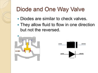
- 3. Diode and One Way Valve Diodes are similar to check valves. They allow fluid to flow in one direction but not the reversed.
- 4. How Diode Works The PN junction consists of P and N material joint together. The area where P material meets the N material is called the junction.
- 5. Current in N-Type Material The flow is made up of electron, similar to the current in copper. The electrons leave the crystal and flow towards the positive terminals of the battery.
- 6. Current Flow in P-Type Material Holes flow within the semiconductor from +ve terminal to -ve. The flow external to the semiconductor is always electron.
- 7. Junction Barrier Both N and P types of semiconductors are electrically neutral. The number of electrons and What happen, the electrons from N material move to P material, thus creating protons is balanced. ++ ions on N material. We expected the The hole transferred to N material. This create a field barriers, ++ at N electrons will material and -- at P material. neutralize and balance the holes, but that do not
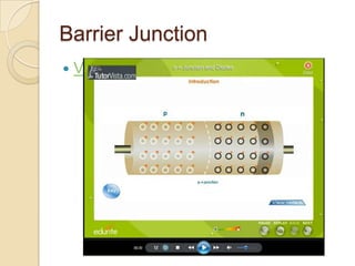
- 8. Barrier Junction Video
- 9. Forward Biased PN Junction
- 10. Reverse Biased PN junction Reverse biased ◦ No current due to majority carrier. ◦ small current due to minority carrier. Resistance characteristic. ◦ Small resistance in forward bias ◦ High resistance in in reversed bias. Refer to the graph.
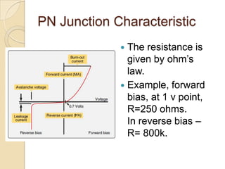
- 11. PN Junction Characteristic The resistance is given by ohm’s law. Example, forward bias, at 1 v point, R=250 ohms. In reverse bias – R= 800k.
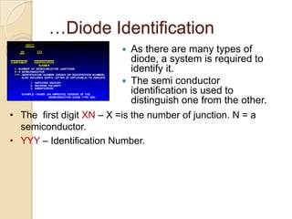
- 12. Diode Identification… As there are many types of diode, a system is required to identify it. The semi conductor identification is used to distinguish one from the other.
- 13. …Diode Identification As there are many types of diode, a system is required to identify it. The semi conductor identification is used to distinguish one from the other. • The first digit XN – X =is the number of junction. N = a semiconductor. • YYY – Identification Number.
- 14. Diode Markings There is the needs to identify anode/cathode The cathode is marked as “k”, “+” or color code or band.
- 15. Diodes Color Code Example ◦ Brown, orange and white bands Brown = 1 Orange = 3 White 9 ◦ So the diode is 1N139
- 17. Diode Maintenance… Diodes are rugged and design to last a long time. Damages can be due to: ◦ Current overloads can damage the junction ◦ Excess voltage ◦ High temperature. Heat increases the current flow which in turn produce more heat which will cause higher current.
- 18. … diode maintenance The followings are the precautions when working with diodes: ◦ Power off when installing and removing diodes ◦ Do not use force to pull the diode from the PCB. ◦ Soldering diode need care to avoid excessive heat. ◦ Replace of diode – must be direct replacement, right direction. ◦ Avoid touching the exposed wires to avoid static electricity.
- 19. Checking Diodes - analogue Checking Diode – Positive lead is black + – Why? + –
- 20. Checking Diodes digital Fwd bias – about 1 Reverse bias – open K circuit.
- 21. Different Types of Diodes
- 22. … Different Types of Diodes ◦ Point Contact Diode ◦ PN Junction ◦ Schottky diodes ◦ Schottky Barrier Diode ◦ Varicap or varactor diode ◦ Zener diode
- 23. Different Types of Diodes … Different types of diodes are manufactured for different purposes: ◦ Laser diode – the diode produces laser light. The laser generation function is cheaper than the alternative, however the diode is more expensive than other types of diodes.
- 24. LED – Light Emitting Diode
- 25. Photodiode When light strikes, it produces electrons or holes causing current flow. Used to detect light. Typically photo-diodes are operated under reverse bias conditions where even small amounts of current flow resulting from the light can be easily detected.
- 26. Diode – PIN Diode The pin diode acts as an ordinary diode at frequencies up to about 100 megahertz, but above this frequency the operational characteristics change. The large intrinsic region increases the transit time of electrons crossing the region. Above 100 megahertz, electrons begin to accumulate in the intrinsic region. The carrier storage in the intrinsic region causes the diode to stop acting as a rectifier and begin acting as a variable resistance.
- 27. Point Contact Diode A point-contact diode works the same as the junction diodes, but their construction is simpler. A block of n-type semiconductor is built, and a conducting sharp-point contact made with some group-3 metal is placed in contact with the semiconductor. Some metal migrates into the semiconductor to make a small region of p-type semiconductor near the contact. The long-popular 1N34 germanium version is still used in radio receivers as a detector and occasionally in specialized analog electronics.
- 28. Schottky Diodes Lower forward voltage drop about 0.15 – 0.4 v Different Construction – metal to semiconductor contact Mainly used for clamping circuit
- 29. Schottky Barrier Diodes Use for rectification Shorter reverse time thus suited for high frequency switching.
- 30. Diode Switching Characteristics When diode is switched from forward biased to reverse biased state or vice versa, it takes finite time to attain a steady state. This time consists of a transient and an inter val of time before the diode attain the steady state is attained. The behavior of the diode during this time is called switching characteristics of the diode. In the forward-bias state, there are a large number of electrons from the n side diffusing to the p side. This diffusion process establishes a large nu mber of minority carriers in each material
- 31. Zener Diode
- 32. RESOURCES CAA UK Recommended Books My Blog Title Author ISBN Aircraft Electricity and Eisman 0-02-801859-1 Electronics Art of Electronics Horowitz 0-521-37095-7 Horowitz /Hill /Hill Elements of Hickey/ 0070286957 Electronics Villines Modern Aviation Helfrich 0-13-118803-8 Electronics Micro Electronics in E Pallet 0-273-08612-X Aircraft systems