SlideShare a Scribd company logo
5
Most read
6
Most read
7
Most read
Name: Dhrumil I. Panchal
Subject: Microprocessor and Interfacing
Branch: Computer Engineering (B.E.)
Year: 2019-20
Instruction cycle(Bus timing diagram) of MVI B, 05H
MVI Instruction
Timing Diagram
Opcode Fetch Cycle
Memory Read Cycle
Frequency
It stores the immediate 8 bit data to a register
or memory location.
Example: MVI B, 05H
Opcode: MVI
Operand: B is the destination register and 05
is the source data which needs to be
transferred to the register.
‘05’ data is stored in the B register.
 Here, opcode is ‘MVI B’ and data is 05.
 Assume the memory address of the opcode and
the data. For example: MVI B, 05
2000: Opcode
2001: 45
 The opcode fetch will be same in all the
instructions.
 Only the read instruction of the opcode needs to
be added in the successive T states.
 For the opcode read the IO/M (low active) = 0,
S1 = 1 and S0 = 0. Also, only 3 T states will be
required.
Timing Diagram of MVI Instruction of 8085 Microprocessor
 00 – lower bit of address where opcode is stored, i.e.,
00
 20 – higher bit of address where opcode is stored,
i.e., 20.
 ALE – Provides signal for multiplexed address and
data bus.
 Only in t1 it used as address bus to fetch lower bit of
address otherwise it will be used as data bus.
 RD (low active) – Signal is 1 in t1, t2 & t4, no data is
read by microprocessor. Signal is 0 in t3, data is read
by microprocessor.
 WR (low active) – Signal is 1 throughout, no data is
written by microprocessor.
 IO/M (low active), S0 and S1 – Signal is 1 in
throughout, operation is performing on input/output.
 00 – lower bit of address where opcode is stored, i.e, 01
 20 – higher bit of address where opcode is stored, i.e, 20.
 ALE – Provides signal for multiplexed address and data
bus. Only in t5 it used as address bus to fetch lower bit of
address otherwise it will be used as data bus.
 RD (low active) – Signal is 1 in t1, t2 & t4, no data is read
by microprocessor. Signal is 0 in t3, data is read by
microprocessor.
 WR (low active) – Signal is 1 throughout, no data is
written by microprocessor.
 IO/M (low active) and S1 – Signal is 1 in throughout,
operation is performing on input/output.
S0 – Signal is 0 throughout, operation is performing on
memory.
Assume that the clock Frequency = 2 MHz
T state = clock period = (1/f) = 0.5 us
Execution Time for
Opcode Fetch = 4*T = 2 us
Memory Read = 3*T = 1.5 us
Total Time = 2+1.5 = 3.5 us
Inspiration from Prof. Parul Bakaraniya
Notes of MI
Book of MI (By Gaonkar)
Images from Google Images
Some My Own Knowledge
Timing Diagram of MVI Instruction of 8085 Microprocessor

More Related Content

What's hot (20)

PPTX
Module4: opamp as a V-I & I-V Converter
chandrakant shinde
 
PDF
Serial communication in 8085
Nitin Ahire
 
PPT
8051 ch9-950217
Gopal Krishna Murthy C R
 
PPTX
NYQUIST CRITERION FOR ZERO ISI
FAIZAN SHAFI
 
PDF
Difference among 8085,8086,80186,80286,80386 Microprocessor.pdf
Mahbubay Rabbani Mim
 
PPTX
System bus timing 8086
mpsrekha83
 
PPTX
Delta Modulation & Adaptive Delta M.pptx
rubini Rubini
 
PPTX
Keyboard Interfacing .pptx
livaunnoor
 
PPTX
Pulse Modulation ppt
sanjeev2419
 
PPT
Programming 8051 Timers
ViVek Patel
 
PPTX
Design of Filters PPT
Imtiyaz Rashed
 
PPTX
Key board interfacing with 8051
DominicHendry
 
PDF
Question paper with solution the 8051 microcontroller based embedded systems...
manishpatel_79
 
PPTX
PIC-18 Microcontroller
ASHISH RANJAN
 
PPTX
Multirate DSP
@zenafaris91
 
PDF
control engineering revision
ragu nath
 
PPTX
Adc and dac
nitugatkal
 
PPTX
Adder
anuppatel111
 
PDF
Fast Fourier Transform
op205
 
PPTX
Differential amplifier
sarunkutti
 
Module4: opamp as a V-I & I-V Converter
chandrakant shinde
 
Serial communication in 8085
Nitin Ahire
 
8051 ch9-950217
Gopal Krishna Murthy C R
 
NYQUIST CRITERION FOR ZERO ISI
FAIZAN SHAFI
 
Difference among 8085,8086,80186,80286,80386 Microprocessor.pdf
Mahbubay Rabbani Mim
 
System bus timing 8086
mpsrekha83
 
Delta Modulation & Adaptive Delta M.pptx
rubini Rubini
 
Keyboard Interfacing .pptx
livaunnoor
 
Pulse Modulation ppt
sanjeev2419
 
Programming 8051 Timers
ViVek Patel
 
Design of Filters PPT
Imtiyaz Rashed
 
Key board interfacing with 8051
DominicHendry
 
Question paper with solution the 8051 microcontroller based embedded systems...
manishpatel_79
 
PIC-18 Microcontroller
ASHISH RANJAN
 
Multirate DSP
@zenafaris91
 
control engineering revision
ragu nath
 
Adc and dac
nitugatkal
 
Adder
anuppatel111
 
Fast Fourier Transform
op205
 
Differential amplifier
sarunkutti
 

Similar to Timing Diagram of MVI Instruction of 8085 Microprocessor (20)

PPTX
timing_diagram_of_8085.pptx
BhagyarajKosamia
 
PPT
8085 Architecture
deval patel
 
PDF
Unit 2 Timing Diagram.pdf
HimanshuPant41
 
PPT
Micro
Brojen Talukdar
 
PPTX
Machine cycles
WafaAbied
 
PPTX
architecture of computer 8085 IO/M addressing mahine cycle and bus
tecmustafa
 
PPTX
A word processor would most likely be used to do which of the following
tecmustafa
 
PPTX
Unit 1 8085 Timing diagram - lecture 5b
Dickson Nkongo
 
PDF
8086 pin.pdfdkdkdkkdldkkkkkkdkdkkdkdkkdk
baijusurya7
 
PPTX
An introduction to microprocessor architecture using INTEL 8085 as a classic...
Prasad Deshpande
 
PPT
Pin diagram of 8085
ShivamSood22
 
PDF
5 pin-diagram-of-8085-181203034237
sunilkumar4879
 
PPTX
Microprocessor history1
HarshitParkar6677
 
PPTX
Microprocessor history1
HarshitParkar6677
 
PPT
8085 Architecture
tsajuraj
 
PPT
8085
tsajuraj
 
PPT
Minimum And Maximum Modes Of 80826
LAVANYA PALANIYAPPAN
 
PPT
architect.ppt
SELVAPRIYAA2
 
PPTX
Microprocessor and Microcontroller.pptx
pvg123456
 
PPT
Timing diagram.ppt
Ganesan Kndsmy
 
timing_diagram_of_8085.pptx
BhagyarajKosamia
 
8085 Architecture
deval patel
 
Unit 2 Timing Diagram.pdf
HimanshuPant41
 
Machine cycles
WafaAbied
 
architecture of computer 8085 IO/M addressing mahine cycle and bus
tecmustafa
 
A word processor would most likely be used to do which of the following
tecmustafa
 
Unit 1 8085 Timing diagram - lecture 5b
Dickson Nkongo
 
8086 pin.pdfdkdkdkkdldkkkkkkdkdkkdkdkkdk
baijusurya7
 
An introduction to microprocessor architecture using INTEL 8085 as a classic...
Prasad Deshpande
 
Pin diagram of 8085
ShivamSood22
 
5 pin-diagram-of-8085-181203034237
sunilkumar4879
 
Microprocessor history1
HarshitParkar6677
 
Microprocessor history1
HarshitParkar6677
 
8085 Architecture
tsajuraj
 
8085
tsajuraj
 
Minimum And Maximum Modes Of 80826
LAVANYA PALANIYAPPAN
 
architect.ppt
SELVAPRIYAA2
 
Microprocessor and Microcontroller.pptx
pvg123456
 
Timing diagram.ppt
Ganesan Kndsmy
 
Ad

More from Dhrumil Panchal (20)

PPTX
YouTube Cryptocurrency Scam
Dhrumil Panchal
 
PPTX
This and Static Keyword
Dhrumil Panchal
 
PPTX
Servlet and Servlet Life Cycle
Dhrumil Panchal
 
PPTX
Properties and Indexers
Dhrumil Panchal
 
PPTX
Chomsky Normal Form
Dhrumil Panchal
 
PPTX
IEEE 802.11 Architecture and Services
Dhrumil Panchal
 
PPTX
Key roles for successful analytic project in Data Mining
Dhrumil Panchal
 
PPTX
Dynamic Programming Code-Optimization Algorithm (Compiler Design)
Dhrumil Panchal
 
PPTX
Different Software Testing Types and CMM Standard
Dhrumil Panchal
 
PPTX
Web Design Issues
Dhrumil Panchal
 
PPTX
Toy Interpreter
Dhrumil Panchal
 
PPTX
Traditional Problems Associated with Computer Crime
Dhrumil Panchal
 
PPTX
Breadth First Search (BFS)
Dhrumil Panchal
 
PPTX
File Management – File Concept, access methods, File types and File Operation
Dhrumil Panchal
 
PPTX
Constructor and Types of Constructors
Dhrumil Panchal
 
PPTX
Types of Instruction Format
Dhrumil Panchal
 
PPTX
Types of Cables(Guided Media for Transmisson)
Dhrumil Panchal
 
PPTX
Global Service for Mobile Communication
Dhrumil Panchal
 
PPTX
Denial of Service Attack
Dhrumil Panchal
 
PPTX
Fourier Series
Dhrumil Panchal
 
YouTube Cryptocurrency Scam
Dhrumil Panchal
 
This and Static Keyword
Dhrumil Panchal
 
Servlet and Servlet Life Cycle
Dhrumil Panchal
 
Properties and Indexers
Dhrumil Panchal
 
Chomsky Normal Form
Dhrumil Panchal
 
IEEE 802.11 Architecture and Services
Dhrumil Panchal
 
Key roles for successful analytic project in Data Mining
Dhrumil Panchal
 
Dynamic Programming Code-Optimization Algorithm (Compiler Design)
Dhrumil Panchal
 
Different Software Testing Types and CMM Standard
Dhrumil Panchal
 
Web Design Issues
Dhrumil Panchal
 
Toy Interpreter
Dhrumil Panchal
 
Traditional Problems Associated with Computer Crime
Dhrumil Panchal
 
Breadth First Search (BFS)
Dhrumil Panchal
 
File Management – File Concept, access methods, File types and File Operation
Dhrumil Panchal
 
Constructor and Types of Constructors
Dhrumil Panchal
 
Types of Instruction Format
Dhrumil Panchal
 
Types of Cables(Guided Media for Transmisson)
Dhrumil Panchal
 
Global Service for Mobile Communication
Dhrumil Panchal
 
Denial of Service Attack
Dhrumil Panchal
 
Fourier Series
Dhrumil Panchal
 
Ad

Recently uploaded (20)

PPTX
Green Building & Energy Conservation ppt
Sagar Sarangi
 
PPTX
265587293-NFPA 101 Life safety code-PPT-1.pptx
chandermwason
 
DOCX
8th International Conference on Electrical Engineering (ELEN 2025)
elelijjournal653
 
PPTX
原版一样(Acadia毕业证书)加拿大阿卡迪亚大学毕业证办理方法
Taqyea
 
PPTX
GitOps_Without_K8s_Training_detailed git repository
DanialHabibi2
 
PPTX
Depth First Search Algorithm in 🧠 DFS in Artificial Intelligence (AI)
rafeeqshaik212002
 
PDF
MAD Unit - 2 Activity and Fragment Management in Android (Diploma IT)
JappanMavani
 
PPTX
Lecture 1 Shell and Tube Heat exchanger-1.pptx
mailforillegalwork
 
PDF
Pressure Measurement training for engineers and Technicians
AIESOLUTIONS
 
PDF
MAD Unit - 1 Introduction of Android IT Department
JappanMavani
 
PPTX
Evaluation and thermal analysis of shell and tube heat exchanger as per requi...
shahveer210504
 
PDF
Basic_Concepts_in_Clinical_Biochemistry_2018كيمياء_عملي.pdf
AdelLoin
 
PPTX
MobileComputingMANET2023 MobileComputingMANET2023.pptx
masterfake98765
 
PPTX
Arduino Based Gas Leakage Detector Project
CircuitDigest
 
PPTX
Element 11. ELECTRICITY safety and hazards
merrandomohandas
 
PPTX
GitOps_Repo_Structure for begeinner(Scaffolindg)
DanialHabibi2
 
PDF
GTU Civil Engineering All Semester Syllabus.pdf
Vimal Bhojani
 
PPT
PPT2_Metal formingMECHANICALENGINEEIRNG .ppt
Praveen Kumar
 
PDF
Biomechanics of Gait: Engineering Solutions for Rehabilitation (www.kiu.ac.ug)
publication11
 
PPTX
Types of Bearing_Specifications_PPT.pptx
PranjulAgrahariAkash
 
Green Building & Energy Conservation ppt
Sagar Sarangi
 
265587293-NFPA 101 Life safety code-PPT-1.pptx
chandermwason
 
8th International Conference on Electrical Engineering (ELEN 2025)
elelijjournal653
 
原版一样(Acadia毕业证书)加拿大阿卡迪亚大学毕业证办理方法
Taqyea
 
GitOps_Without_K8s_Training_detailed git repository
DanialHabibi2
 
Depth First Search Algorithm in 🧠 DFS in Artificial Intelligence (AI)
rafeeqshaik212002
 
MAD Unit - 2 Activity and Fragment Management in Android (Diploma IT)
JappanMavani
 
Lecture 1 Shell and Tube Heat exchanger-1.pptx
mailforillegalwork
 
Pressure Measurement training for engineers and Technicians
AIESOLUTIONS
 
MAD Unit - 1 Introduction of Android IT Department
JappanMavani
 
Evaluation and thermal analysis of shell and tube heat exchanger as per requi...
shahveer210504
 
Basic_Concepts_in_Clinical_Biochemistry_2018كيمياء_عملي.pdf
AdelLoin
 
MobileComputingMANET2023 MobileComputingMANET2023.pptx
masterfake98765
 
Arduino Based Gas Leakage Detector Project
CircuitDigest
 
Element 11. ELECTRICITY safety and hazards
merrandomohandas
 
GitOps_Repo_Structure for begeinner(Scaffolindg)
DanialHabibi2
 
GTU Civil Engineering All Semester Syllabus.pdf
Vimal Bhojani
 
PPT2_Metal formingMECHANICALENGINEEIRNG .ppt
Praveen Kumar
 
Biomechanics of Gait: Engineering Solutions for Rehabilitation (www.kiu.ac.ug)
publication11
 
Types of Bearing_Specifications_PPT.pptx
PranjulAgrahariAkash
 

Timing Diagram of MVI Instruction of 8085 Microprocessor

  • 1. Name: Dhrumil I. Panchal Subject: Microprocessor and Interfacing Branch: Computer Engineering (B.E.) Year: 2019-20
  • 2. Instruction cycle(Bus timing diagram) of MVI B, 05H
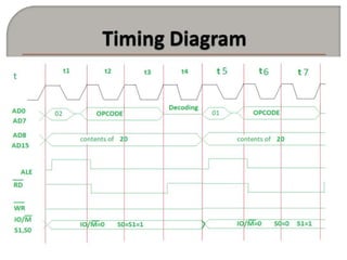
  • 3. MVI Instruction Timing Diagram Opcode Fetch Cycle Memory Read Cycle Frequency
  • 4. It stores the immediate 8 bit data to a register or memory location. Example: MVI B, 05H Opcode: MVI Operand: B is the destination register and 05 is the source data which needs to be transferred to the register. ‘05’ data is stored in the B register.
  • 5.  Here, opcode is ‘MVI B’ and data is 05.  Assume the memory address of the opcode and the data. For example: MVI B, 05 2000: Opcode 2001: 45  The opcode fetch will be same in all the instructions.  Only the read instruction of the opcode needs to be added in the successive T states.  For the opcode read the IO/M (low active) = 0, S1 = 1 and S0 = 0. Also, only 3 T states will be required.
  • 7.  00 – lower bit of address where opcode is stored, i.e., 00  20 – higher bit of address where opcode is stored, i.e., 20.  ALE – Provides signal for multiplexed address and data bus.  Only in t1 it used as address bus to fetch lower bit of address otherwise it will be used as data bus.  RD (low active) – Signal is 1 in t1, t2 & t4, no data is read by microprocessor. Signal is 0 in t3, data is read by microprocessor.  WR (low active) – Signal is 1 throughout, no data is written by microprocessor.  IO/M (low active), S0 and S1 – Signal is 1 in throughout, operation is performing on input/output.
  • 8.  00 – lower bit of address where opcode is stored, i.e, 01  20 – higher bit of address where opcode is stored, i.e, 20.  ALE – Provides signal for multiplexed address and data bus. Only in t5 it used as address bus to fetch lower bit of address otherwise it will be used as data bus.  RD (low active) – Signal is 1 in t1, t2 & t4, no data is read by microprocessor. Signal is 0 in t3, data is read by microprocessor.  WR (low active) – Signal is 1 throughout, no data is written by microprocessor.  IO/M (low active) and S1 – Signal is 1 in throughout, operation is performing on input/output. S0 – Signal is 0 throughout, operation is performing on memory.
  • 9. Assume that the clock Frequency = 2 MHz T state = clock period = (1/f) = 0.5 us Execution Time for Opcode Fetch = 4*T = 2 us Memory Read = 3*T = 1.5 us Total Time = 2+1.5 = 3.5 us
  • 10. Inspiration from Prof. Parul Bakaraniya Notes of MI Book of MI (By Gaonkar) Images from Google Images Some My Own Knowledge