SlideShare a Scribd company logo
Computer Organization
First Year BCA Science
Subject Code : BCA- 121
Subject Teacher : Asst. Prof. Amruta Bhandari
UNIT 4
INTRODUCTION TO
SEQUENTIALLOGIC CIRCUITS
SEQUENTIAL LOGIC CIRCUITS
SEQUENTIALLOGIC CIRCUITS
Sequential logic circuit consists of a combinational circuit with
storage elements connected as a feedback to combinationalcircuit
• output depends on the sequence of inputs (past andpresent)
• stores information (state) from past inputs
SEQUENTIAL LOGIC CIRCUITS
Figure 1: Sequential logic circuits
SEQUENTIAL LOGIC CIRCUITS
• Output depends on
– Input
– Previous state of the circuit
• Flip-flop: basic memory
element
• State table: output for all
combinations of input and
previous states(TruthTable)
SEQUENTIAL LOGIC CIRCUITS
1. Sequential circuit receives the binary informationfrom
external inputs and with the present state of the storage
elements together determine the binary value of the
outputs.
2. The output in a sequential circuit are a function of not
only the inputs, but also the present state of the storage
elements.
3. The next state of the storage elements is also afunction
of external inputs and the presentstate.
4. There are two main types of sequentialcircuits
1. synchronous sequential circuits
2. asynchronous sequential circuits
Synchronous sequential circuits
It is a system whose behaviour can be
defined from the knowledge of itssignals
at discrete instants of time
Asynchronous sequential circuits
It depends upon the input signals at any
instant of time and the order in which the
input changes
SEQUENTIAL LOGIC CIRCUITS
Combinational vs. Sequential
COMBINA
TIONAL LOGIC CIRCUIT
Combinational logic circuit consists of input variables, logic gates
and output variables. The logic gate accepts signals from the inputs
and generates signals to the outputs.
n input
variables
m output
variables
For n input variables there are 2n possible combinations of binary input variables
SEQUENTIALLOGIC CIRCUITS
Sequential logic circuit consists of a combinational circuit with
storage elements connected as a feedback to combinationalcircuit
• output depends on the sequence of inputs (past andpresent)
• stores information (state) from past inputs
Combinational vs. Sequential
Figure 1: Sequential logic circuits
Combinational vs. Sequential
Combinational Circuit
always gives the same output for a given set of inputs
ex: adder always generates sum and carry,
regardless of previous inputs
Sequential Circuit
stores information
output depends on stored information (state) plus input
so a given input might produce different outputs,
depending on the stored information
example: ticket counter
advances when you push the button
output depends on previous state
useful for building ―memory‖ elements and ―statemachines‖
Combinational vs. Sequential
LATCHES
STORAGE ELEMENTS
Storage elements in a digital circuit can maintain a binary state
indefinitely, until directed by an input signal to switch states. The
major difference among various storage elements are the number of
input they posses and the manner in which the inputs affect the
binary state.There are two types of storage elements
1. Latches
2. Flipflops
Storage elements that operate with signal level are referred aslatch
and those controlled by a clock transition are referred asflipflops.
LATCHES
1. LATCHES:
A latch has a feedback path, so information can be retained by the device.
Therefore latches can be memory devices, and can store one bit of data for
as long as the device is powered. As the name suggests, latches are used to
"latch onto" information and hold in place. Latches are very similar
to flip-flops, but are not synchronous devices, and do not operate on clock
edges as flip-flops do. Latch is a level sensitive device. Latch is a
monostable multivibrator
2. FLIPFLOPS:
A flip-flop is a circuit that has two stable states and can be used to store state
information. A flip-flop is a bistable multivibrator. The circuit can be made to
change state by signals applied to one or more control inputs and will have one
or two outputs. It is the basic storage element in sequential logic. Flip-flops and
latches are fundamental building blocks of digital electronics systems used in
computers, communications, and many other types of systems. Flipflop is a
edge sensitive device.
LATCHES
SR LATCH
An SR latch (Set/Reset) is an asynchronous device: it works independently of control
signals and relies only on the state of the S and R inputs. In the image we can see that an
SR flip-flop can be created with two NOR gates that have a cross-feedback loop. SR
latches can also be made from NAND gates, but the inputs are swapped and negated. In
this case, it is sometimes called an SR latch.
R is used to ―reset‖ or ―clear‖ the element – set it to zero. S is used to ―set‖ the element –
set it to one.
If both R and S are one, out could be either zero or one. ―quiescent‖ state -- holds its
previous value. note: if a is 1, b is 0, and vice versa
LATCHES
GA
TED D-LA
TCH
The D latch (D for "data") or transparent latch is a simple extension of the gated SR
latch that removes the possibility of invalid input states. Two inputs: D (data) and WE
(write enable)
when WE = 1, latch is set to value of D
S = NOT(D), R = D
when WE = 0, latch holds previous value
S = R = 1
FLIP FLOPS:RS FLIP FLOP
Flip flops
A flip flop is an electronic circuit with two stable states that can be used to store
binary data. The stored data can be changed by applying varying inputs. Flip-flops
and latches are fundamental building blocks of digital electronics systems used in
computers, communications, and many other types of systems. Flip-flops and
latches are used as data storage elements. There are 4 types of flipflops
1. RS flip flop
2. Jk flip flop
3. D flip flop
4. T flip flop
Applications of Flip-Flops
These are the various types of flip-flops being used in digital electronic circuits and
the applications like Counters, Frequency Dividers, Shift Registers, Storage
Registers
FLIP FLOPS:RS FLIP FLOP
EDGE-TRIGGERED FLIP FLOPS
Characteristics
- State transition occurs at the rising edge or
falling edge of the clock pulse
Latches
respond to the input only during these periods
Edge-triggered Flip Flops (positive)
respond to the input only at this time
FLIP FLOPS:RS FLIP FLOP
FLIPFLOPS
FLIPFLOPS:RS FLIPFLOP
SR Flip-Flop
The SR flip-flop, also known as a SR Latch, can be considered as one of the most basic
sequential logic circuit possible. This simple flip-flop is basically a one-bit memory bistable
device that has two inputs, one which will ―SET‖ the device (meaning the output = ―1‖),
and is labelled S and one which will ―RESET‖the device (meaning the output = ―0‖),
labelled R.The reset input resets the flip-flop back to its original state with an output Q that
will be either at a logic level ―1‖or logic ―0‖depending upon this set/resetcondition.
Abasic NAND gate SR flip-flop circuit provides feedback from both of its outputs back to
its opposing inputs and is commonly used in memory circuits to store a single data bit.
Then the SR flip-flop actually has three inputs, Set, Reset and its current output Q relating
to it’s current state or history.
Truth Table for this Set-Reset Function
FLIPFLOPS:JK FLIPFLOP
JK Flip flop
The JK Flip-flop is similar to the SR Flip-flop but there is no change in state when
the J and K inputs are both LOW.The basic S-R NAND flip-flop circuit has many
advantages and uses in sequential logic circuits but it suffers from two basic
switching problems.
1. the Set = 0 and Reset = 0 condition (S = R = 0) must always be avoided
2.if Set or Reset change state while the enable (EN) input is high the correct
latching action may not occur
Then to overcome these two fundamental design problems with the SR flip-flop
design, the JK flip Flop was developed by the scientist name Jack Kirby.
The JK flip flop is basically a gated SR flip-flop with the addition of a clock input
circuitry that prevents the illegal or invalid output condition that can occur when
both inputs S and R are equal to logic level ―
1‖. Due to this additional clocked
input, a JK flip-flop has four possible input combinations, ―logic1‖, ―logic0‖, ―
n
o
change‖ and ―toggle‖.The symbol for a JK flip flop is similar to that of an SR
Bistable Latch as seen in the previous tutorial except for the addition of a clock
input.
FLIPFLOPS:JK FLIPFLOP
Both the S and the R inputs of the previous SR bistable have now been replaced by two inputs
called the J and K inputs, respectively after its inventorJack Kilby. Then thisequates
to: J = S and K = R.
The two 2-inputAND gates of the gated SR bistable have now been replaced by two 3-
input NAND gates with the third input of each gate connected to the outputs at Q and Q. This cross
coupling of the SR flip-flop allows the previously invalid condition of S = ―1‖and R = ―1‖state to be
used to produce a ―toggle action‖ as the two inputsare now interlocked.
If the circuit is now ―SET‖ the J input is inhibited by the ―0‖status of Q throughthe
lower NAND gate. If the circuit is ―RESET‖ the K input is inhibited by the ―0‖status of Q through
the upper NAND gate.As Q and Q are always different we can use them to control the input.When
both inputs J and K are equal to logic ―1‖,the JK flip flop toggles as shown in the following truth
table.
FLIPFLOPS:JK FLIPFLOP
The Truth T
able for the JK Function
Then the JK flip-flop is basically an SR flip flop
with feedback which enables only one of its two
input terminals, either SET or RESET to be
active at any one time thereby eliminating the
invalid condition seen previously in the SR flip
flop circuit. Also when both the J and
the K inputs are at logic level ―
1‖ at the same
time, and the clock input is pulsed ―HIGH‖,the
circuit will ―
toggle‖ from its SET state to a
RESET state, or visa-versa. This results in the JK
flip flop acting more like a T-type toggle flip-flop
when both terminals are―HIGH‖.
FLIPFLOPS:T FLIPFLOP
T FLIPFLOP
We can construct a T flip flop by any of the following methods. Connecting the output feedback
to the input, in SR flip flop. Connecting the XOR of T input and Q PREVIOUS output to the
Data input, in D flip flop. Hard – wiring the J and K inputs together and connecting it to T input,
in JK flip – flop.
FLIPFLOPS:T FLIPFLOP
Working
T flip – flop is an edge triggered device i.e. the low to high or high to low transitions
on a clock signal of narrow triggers that is provided as input will cause the change in
output state of flip – flop. T flip – flop is an edge triggered device.
Truth T
able of T flip – flop
FLIPFLOPS:T FLIPFLOP
If the output Q = 0, then the upper NAND is in enable state and lower NAND gate is in
disable condition. This allows the trigger to pass the S inputs to make the flip – flop in SET
state i.e. Q = 1.
If the output Q = 1, then the upper NAND is in disable state and lower NAND gate is in
enable condition. This allows the trigger to pass the R inputs to make the flip – flop in RESET
state i.e. Q =0.
In simple terms, the operation of the T flip – flop is
When the T input is low, then the next sate of the T flip flop is same as the present state.
T = 0 and present state = 0 then the next state = 0
T = 1 and present state = 1 then the next state = 1
When the T input is high and during the positive transition of the clock signal, the next stateof
the T flip – flop is the inverse of presentstate.
T = 1 and present state = 0 then the next state = 1
T = 1 and present state = 1 then the next state = 0
Applications
Frequency Division Circuits.
2 – Bit Parallel Load Registers.
FLIPFLOPS:D FLIPFLOP
D FLIP FLOP
The D-type flip-flop is a modified Set-Reset flip-flop with the addition of an inverter to prevent
the S and R inputs from being at the same logic level
One of the main disadvantages of the basic SR NAND Gate Bistable circuit is that the
indeterminate input condition of SET = ―0‖and RESET = ―0‖isforbidden.
This state will force both outputs to be at logic ―1‖,over-riding the feedback latching action and
whichever input goes to logic level ―1‖first will lose control, while the other input still at logic
―
0‖ controls the resulting state of the latch.
But in order to prevent this from happening an inverter can be connected between the ―SET‖ and
the ―RESET‖inputs to produce another type of flip flop circuit known as a Data Latch, Delay
flip flop, D-type Bistable, D-type Flip Flop or just simply a D Flip Flop as it is more generally
called.
The D Flip Flop is by far the most important of the clocked flip-flops as it ensures that ensures
that inputs S and R are never equal to one at the same time. The D-type flip flop are constructed
from a gated SR flip-flop with an inverter added between the S and the R inputs to allow for a
single D (data) input.
Then this single data input, labelled ―D‖and is used in place of the ―Set‖ signal, and the inverter
is used to generate the complementary ―Reset‖input thereby making a level-sensitive D-type
flip-flop from a level-sensitive SR-latch as now S = D and R = not D as shown.
FLIPFLOPS:D FLIPFLOP
D-type Flip-Flop Circuit
Weremember that a simple SR flip-flop requires two inputs, one to ―SET‖ the output and one
to ―RESET‖ the output. By connecting an inverter (NOT gate) to the SR flip-flop we can
―SET‖and ―RESET‖the flip-flop using just one input as now the two input signals are
complements of each other. This complement avoids the ambiguity inherent in the SR latch
when both inputs are LOW, since that state is no longer possible. Thus this single input is
called the ―DA
T
A‖input. If this data input is held HIGH the flip flop would be ―SET‖and
when it is LOW the flip flop would change and become ―RESET‖. However, this would be
rather pointless since the output of the flip flop would always change on every pulse applied
to this data input.
FLIPFLOPS:D FLIPFLOP
To avoid this an additional input called the ―CLOCK‖ or ―ENABLE‖ input is used to isolate the
data input from the flip flop’s latching circuitry after the desired data has been stored. The effect
is that D input condition is only copied to the output Q when the clock input is active. This then
forms the basis of another sequential device called a D Flip Flop.
The ―
Dflip flop‖ will store and output whatever logic level is applied to its data terminal so long
as the clock input is HIGH. Once the clock input goes LOW the ―set‖and ―reset‖inputs of the
flip-flop are both held at logic level ―1‖so it will not change state and store whatever data was
present on its output before the clock transition occurred. In other words the output is ―latched‖at
either logic ―0‖or logic ―1‖.
Truth Table for the D-type Flip Flop
Note that: ↓ and ↑ indicates direction of
clock pulse as it is assumed D-type flip
flops are edge triggered
FLIPFLOPS:MASTER SLAVE FLIPFLOP
MASTER SLAVE FLIPFLOP
Master-slave flip flop is designed using two separate flip flops. Out of these, one acts as
the master and the other as a slave. The figure of a master-slave J-K flip flop is shown
below.
From the above figure you can see that both the J-K flip flops are presented in a
series connection. The output of the master J-K flip flop is fed to the input of the slave
J-K flip flop. The output of the slave J-K flip flop is given as a feedback to the input of
the master J-K flip flop. The clock pulse [Clk] is given to the master J-K flip flop and it
is sent through a NOT Gate and thus inverted before passing it to the slave J-K flip
flop.
FLIPFLOPS:MASTER SLAVE FLIPFLOP
The truth table corresponding to the working of the flip-flop shown in Figure is given by
TableI. Here it is seen that the outputs at the master-part of the flip-flop (data enclosed
in red boxes) appear during the positive-edge of the clock (red arrow). However at this
instant the slave-outputs remain latched or unchanged. The same data is transferred to
the output pins of the master-slave flip-flop (data enclosed in blue boxes) by the slave
during the negative edge of the clock pulse (blue arrow). The same principle is further
emphasized in the timing diagram of master-slave flip-flop shown by Figure 3. Here
the green arrows are used to indicate that the slave-output is nothing but the master-
output delayed by half-a-clock cycle. Moreover it is to be noted that the working of any
other type of master-slave flip-flop is analogous to that of the master slave JK flip-flop
explained here.
FLIPFLOPS:MASTER SLAVE FLIPFLOP
.
FLIPFLOPS:EXCITATION FUNCTIONS
In electronics design, an excitation table shows the minimum inputs that are necessary to generate a
particular next state (in other words, to "excite" it to the next state) when the current state is known.
They are similar to truth tables and state tables, but rearrange the data so that the current state and next
state are next to each other on the left-hand side of the table, and the inputs needed to make that state
change happen.
All flip-flops can be divided into four basic types: SR, JK, D and T. They differ in the number of
inputs and in the response invoked by different value of inputsignals.
The characteristic table in the third column of Table 1 defines the state of each flip-flop as a function of
its inputs and previous state. Q refers to the present state and Q(next) refers to the next state after the
occurrence of the clock pulse. The characteristic table for the RS flip-flop shows that the next state is
equal to the present state when both inputs S and R are equal to 0. When R=1, the next clock pulse
clears the flip-flop. When S=1, the flip-flop output Q is set to 1. The equation mark (?) for the next state
when S and R are both equal to 1 designates an indeterminate nextstate.
The characteristic table for the JK flip-flop is the same as that of the RS when J and K are replaced by S
and R respectively, except for the indeterminate case. When both J and K are equal to 1, the next state is
equal to the complement of the present state, that is, Q(next) = Q'.
The next state of the D flip-flop is completely dependent on the input D and independent of the present
state.
The next state for the T flip-flop is the same as the present state Q if T=0 and complemented ifT=1.
SR Flip flop
FLIPFLOPS:EXCITATION FUNCTIONS
FLIP-FLOPSYMBOL CHARACTERISTIC TABLE
CHARACTERISTIC EQUATION EXCITA
TION TABLE
JK Flip flop
FLIPFLOPS:EXCITATION FUNCTIONS
FLIP-FLOPSYMBOL CHARACTERISTIC TABLE
CHARACTERISTIC EQUATION EXCITA
TION TABLE
D Flip flop
FLIPFLOPS:EXCITATION FUNCTIONS
FLIP-FLOPSYMBOL CHARACTERISTIC TABLE
CHARACTERISTIC EQUATION EXCITA
TION TABLE
T Flip flop
FLIPFLOPS:EXCITATION FUNCTIONS
FLIP-FLOPSYMBOL CHARACTERISTIC TABLE
CHARACTERISTIC EQUATION EXCITA
TION TABLE
CONVERTION OF ONE FLIP FLOP TO ANOTHER FLIP FLOP
CONVERTION OF SR FLIPFLOPTO JK FLIPFLOP
J and K will be given as external inputs to S and R. As shown in the logic diagram below, S
and R will be the outputs of the combinationalcircuit.
The truth tables for the flip flop conversion are given below. The present state is represented
by Qp and Qp+1 is the next state to be obtained when the J and K inputs are applied.
For two inputs J and K, there will be eight possible combinations. For each combination of
J, K and Qp, the corresponding Qp+1 states are found. Qp+1 simply suggests the future
values to be obtained by the JK flip flop after the value of Qp. The table is then completed
by writing the values of S and R required to get each Qp+1 from the corresponding Qp. That
is, the values of S and R that are required to change the state of the flip flop from Qp to
Qp+1 are written.
CONVERTION OF ONE FLIP FLOP TO ANOTHER FLIP FLOP
CONVERTION OF JK FLIPFLOPTO SR FLIPFLOP
This will be the reverse process of the above explained conversion. S and R will be the
external inputs to J and K. As shown in the logic diagram below, J and K will be the
outputs of the combinational circuit. Thus, the values of J and K have to be obtained in
terms of S, R and Qp. The logic diagram is shown below.
A conversion table is to be written using S, R, Qp, Qp+1, J and K. For two inputs, S and
R, eight combinations are made. For each combination, the corresponding Qp+1 outputs
are found ut. The outputs for the combinations of S=1 and R=1 are not permitted for an
SR flip flop. Thus the outputs are considered invalid and the J and K values are taken as
―
don’t cares‖.
CONVERTION OF ONE FLIP FLOP TO ANOTHER FLIP FLOP
CONVERTION OF SR FLIPFLOPTO D FLIPFLOP
As shown in the figure, S and R are the actual inputs of the flip flop and D is the external
input of the flip flop. The four combinations, the logic diagram, conversion table, and the
K-map for S and R in terms of D and Qp are shown below.
CONVERTION OF ONE FLIP FLOP TO ANOTHER FLIP FLOP
CONVERTION OF D FLIPFLOPTO SR FLIPFLOP
D is the actual input of the flip flop and S and R are the external inputs. Eight possible
combinations are achieved from the external inputs S, R and Qp. But, since the combination
of S=1 and R=1 are invalid, the values of Qp+1 and D are considered as ―don’tcares‖. The
logic diagram showing the conversion from D to SR, and the K-map for D in terms of S, R
and Qp are shown below.
CONVERTION OF ONE FLIP FLOP TO ANOTHER FLIP FLOP
CONVERTION OFJK FLIPFLOPTO T FLIPFLOP
J and K are the actual inputs of the flip flop and T is taken as the external input for
conversion. Four combinations are produced with T and Qp. J and K are expressed in terms
of T and Qp. The conversion table, K-maps, and the logic diagram are given below.
CONVERTION OF ONE FLIP FLOP TO ANOTHER FLIP FLOP
CONVERTION OF JK FLIPFLOPTO D FLIPFLOP
D is the external input and J and K are the actual inputs of the flip flop. D and Qp make
four combinations. J and K are expressed in terms of D and Qp. The four combination
conversion table, the K-maps for J and K in terms of D and Qp, and the logic diagram
showing the conversion from JK to D are given below.
CONVERTION OF ONE FLIP FLOP TO ANOTHER FLIP FLOP
CONVERTION OF D FLIPFLOPTO JK FLIPFLOP
In this conversion, D is the actual input to the flip flop and J and K are the external inputs.
J, K and Qp make eight possible combinations, as shown in the conversion table below. D
is expressed in terms of J, K and Qp.
The conversion table, the K-map for D in terms of J, K and Qp and the logic diagram
showing the conversion from D to JK are given in the figure below.
CONVERTION OF ONE FLIP FLOP TO ANOTHER FLIP FLOP
CONVERTION OFT FLIPFLOPTO JK FLIPFLOP
Webegin with the T-to-JK conversion table (see Figure 5), which combines the information
in the JK flip-flop's truth table and the T flip-flop's excitation table.
Next, we need to obtain the simplified Boolean expression for the T input in terms of J, K, and
Qn. The expression for the T input as JQ̅ n + KQn. This means that to convert the T flip-flop into
a JK flip-flop, the T input is driven by the output of a two-input OR gate which has as inputs
JANDed with the negation of the present-state Qn, i.e., Q̅n
KANDed with the present-state, Qn
STATE MACHINES
State Machine
Another type of sequential circuit
Combines combinational logic with storage
―Remembers‖ state, and changes output (and state) based on inputs and current state
State
The state of a system is a snapshot of all the relevant elements of the system at the moment the
snapshot is taken.
Examples:
The state of a basketball game can be represented by the scoreboard.
Number of points, time remaining, possession, etc.
The state of a tic-tac-toe game can be represented by the placement of X’s and O’s on the board.
STATE MACHINES
State Tables and State Diagrams
ST
A
TETABLESAND ST
A
TE DIAGRAMS
In this model the effect of all previous inputs on the outputs is represented by a state of the
circuit. Thus, the output of the circuit at any time depends upon its current state and the
input. These also determine the next state of the circuit. The relationship that exists among
the inputs, outputs, present states and next states can be specified by either the state table or
the state diagram.
State T
able
The state table representation of a sequential circuit consists of three sections labeled present
state, next state and output. The present state designates the state of flip-flops before the
occurrence of a clock pulse. The next state shows the states of flip-flops after the clock
pulse, and the output section lists the value of the output variables during the presentstate.
STATE MACHINES
State Diagram
In addition to graphical symbols, tables or equations, flip-flops can also be represented
graphically by a state diagram. In this diagram, a state is represented by a circle, and the
transition between states is indicated by directed lines (or arcs) connecting the circles.
The binary number inside each circle identifies the state the
circle represents. The directed lines are labelled with two binary
numbers separated by a slash (/). The input value that causes the
state transition is labelled first. The number after the slash
symbol / gives the value of the output. For example, the directed
line from state 00 to 01 is labelled 1/0, meaning that, if the
sequential circuit is in a present state and the input is 1, then the
next state is 01 and the output is 0. If it is in a present state 00
and the input is 0, it will remain in that state. A directed line
connecting a circle with itself indicates that no change of state
occurs. The state diagram provides exactly the same information
as the state table and is obtained directly from the state table.
State Diagram
Example:
Consider a sequential circuit
STATE MACHINES
The behavior of the circuit is determined by the
following Boolean expressions:
Z = x*Q1
D1 = x' + Q1
D2 = x*Q2' +x'*Q1'
These equations can be used to form the state table. Suppose the present state (i.e. Q1Q2) = 00
and input x = 0. Under these conditions, we get Z = 0, D1 = 1, and D2 = 1. Thus the next state
of the circuit D1D2 = 11, and this will be the present state after the clock pulse has been
applied. The output of the circuit corresponding to the present state Q1Q2 = 00 and x = 1 is Z=
0. This data is entered into the state table as shown in Table2.
State table for the sequential circuit
STATE MACHINES
The state diagram for the sequential circuit
state diagrams of the four types of flip-flops
STA
TE MACHINES
STATE REDUCTION
State Reduction
Any design process must consider the problem of minimising the cost of the final circuit. The
two most obvious cost reductions are reductions in the number of flip-flops and the number of
gates.
The number of states in a sequential circuit is closely related to the complexity of the resulting
circuit. It is therefore desirable to know when two or more states are equivalent in all aspects.
The process of eliminating the equivalent or redundant states from a state table/diagram is
known as state reduction.
Example: Let us consider the state table of a sequentialcircuit
State table
STATE REDUCTION
It can be seen from the table that the present state A and F both have the same next states, B
(when x=0) and C (when x=1). They also produce the same output 1 (when x=0) and 0 (when
x=1). Therefore states A and F are equivalent. Thus one of the states, A or F can be removed
from the state table. For example, if we remove row F from the table and replace all F's by
A's in the columns, the state table is modified
State F removed
It is apparent that states B and E are equivalent. Removing E and replacing E's by B's results
in the reduce table
STATE REDUCTION
Reduced state table
The removal of equivalent states has reduced the number of states in the circuit from six to
four. Two states are considered to be equivalent if and only if for every input sequence the
circuit produces the same output sequence irrespective of which one of the two states is the
starting state.
STATEASSIGNMENT
STATEASSIGNMENT
Each circuit state given in a state table has to be assigned a unique value, which represents
combinations of flip – flop output states.
Acircuit having 2 internal states requires one flip – flop in its implementation
Acircuit having 3 or 4 internal states requires two flip – flops in its implementation
Acircuit having 5→ 8 internal states requires three flip – flops in its implementation etc.
It should be noted that although assignments are arbitrary, one assignment might be more
economical than another.
Consider the state table shown below for a circuit having two input pulses x1, x2 and a level
output Z.
Since the circuit has four internal states then two flip-flops are required. Let the two flip-flop
outputs be represented by variables y1 and y2, which can have combinations of values y1y2 =
00, 01, 11, 10. The state table can then be translated into a state table with secondary
assignments as shown. Note that this is just one of many possible assignments (in fact there are
24)
STATEASSIGNMENT
Example of state assignment
With y1y2 =0 (i.e. in state 1), if x1 is applied then y1y2must change to 01 (i.e. state 2). That is,
the flip/flop generating y1 must not disturbed, but the y2generating flip-flop requires an input
such that the circuit settles in state 2, (for example a SET input if using SR flip-flops).
MEALY AND MOORE STATEMACHINES
Mealy state machine
In the theory of computation, a Mealy machine is a finite state transducer that generates an
output based on its current state and input. This means that the state diagram will include
both an input and output signal for each transition edge. In contrast, the output of a Moore
finite state machine depends only on the machine's current state; transitions are not directly
dependent upon input. The use of a Mealy FSM leads often to a reduction of the number of
states. However, for each Mealy machine there is an equivalent Moore machine.
MEALY AND MOORE STATEMACHINES
Moore state machine
In the theory of computation, a Moore machine is a finite state transducer where the outputs are
determined by the current state alone (and do not depend directly on the input). The state diagram
for a Moore machine will include an output signal for each state. Compare with a Mealy machine,
which maps transitions in the machine to outputs. The advantage of the Moore model is a
simplification of the behavior.
MEALY AND MOORE STATEMACHINES
Examples for Mealy and Moore machines
Derive a minimal state table for a single-input and single-output Moore-type FSM
that produces an output of 1 if in the input sequence it detects either 110 or 101
patterns. Overlapping sequences should be detected. (Show the detailed stepsof
your solution.)
MEAL
YAND MOORE STA
TEMACHINES
Sate Table (MooreFSM)
MEALY AND MOORE STATEMACHINES
StateAssignment (Mealy FSM):
stateA: Got no 1
state B: Got‖1‖
state C: Got‖11‖
state D: Got‖10”
Sate Table (Mealy FSM)
MEALY AND MOORE MACHINES
Sequential Logic Implementation
Models for representing sequential circuits
Abstraction of sequential elements
Finite state machines and their state diagrams
Inputs/outputs
Mealy, Moore, and synchronous Mealy machines
Finite state machine design procedure
V
erilog specification
Deriving state diagram
Deriving state transition table
Determining next state and output functions
Implementing combinational logic
MEALY AND MOORE MACHINES
Mealy vs. Moore Machines
Moore: outputs depend on current state only
Mealy: outputs depend on current state and inputs
Ant brain is a Moore Machine (Output does not react immediately to input change)
Wecould have specified a Mealy FSM (Outputs have immediate reaction to inputs .As
inputs change, so does next state, doesn’t commit until clocking event)
Specifying Outputs for a Moore Machine
Output is only function of state. Specify in state bubble in state diagram. Example:
sequence detector for 01 or 10
MEALY AND MOORE MACHINES
Specifying Outputs for a Mealy Machine
Output is function of state and inputs .Specify output on transition arc between states.
Example: sequence detector for 01 or 10
MEALY AND MOORE MACHINES
Comparison of Mealy and Moore Machines
Mealy Machines tend to have less states
Different outputs on arcs (n^2) rather than states (n)
Moore Machines are safer to use
Outputs change at clock edge (always one cycle later)
In Mealy machines, input change can cause output change as soon as logic is done – a big
problem when two machines are interconnected – asynchronous feedback
Mealy Machines react faster to inputs
React in same cycle – don't need to wait for clock
In Moore machines, more logic may be necessary to decode state into outputs – more gate
delays after
SYNCHRONOUSAND ASYNCHRONOUS SEQUENTIAL CIRCUITS
synchronous sequential circuits a clock signal consisting of
pulses, controls the
state variables which are represented by flip-flops. they are said to operatein
pulse mode.
asynchronous circuits state changes are not triggered by clock pulses. they depend
on
the values of the input and feedback variables.
two conditions for proper operation:
1.-inputs to the circuit must change one at a time and must remain constant until the
circuit reaches stable state.
2.-feedback variables should change also one at a time. when all internal signals stop
changing, then the circuit is said to have reached stable state when the inputs
satisfy condition 1 above, then the circuit is said to operate in fundamental
mode.
Analysis of Clocked Sequential Circuits
The analysis of a sequential circuit consists of obtaining a table or a diagram for
the time sequence of inputs, outputs, and internal states. It is also possible to
write Boolean expressions that describe the behavior of the sequential circuit.
These expressions must include the necessary time sequence, either directly
or indirectly.
SYNCHRONOUS AND ASYNCHRONOUS SEQUENTIAL CIRCUITS
State Equations
The behavior of a clocked sequential circuit can be described algebraically by means of
state equations. A state equation specifies the next state as a function of the present state and
inputs. Consider the sequential circuit shown in Fig. 5-15. It consists of two D flip-flops A
and B, an input x and an output y.
State equation
A(t+1) =A(t) x(t) + B(t) x(t)
B(t+1) =A`(t) x(t)
A state equation is an algebraic expression that specifies the condition for a flip-flop state
transition. The left side of the equation with (t+1) denotes the next state of the flip-flop one
clock edge later. The right side of the equation is Boolean expression that specifies the
present state and input conditions that make the next state equal to 1.
Y(t) = (A(t) + B(t)) x(t)`
SYNCHRONOUS AND ASYNCHRONOUS SEQUENTIAL CIRCUITS
State Table
The time sequence of inputs, outputs, and flip-flop states can be enumerated in a state table
(sometimes called transition table). State Diagram
1/0 : means input=1
output=0
The information available in a state table can be represented graphically in the form of a state
diagram. In this type of diagram, a state is represented by a circle, and the transitions between
states are indicated by directed lines connecting the circles.
SYNCHRONOUS AND ASYNCHRONOUS SEQUENTIAL CIRCUITS
Flip-Flop Input Equations
The part of the combinational circuit that generates external outputs is descirbed
algebraically by a set of Boolean functions called output equations. The part of
the circuit that generates the inputs to flip-flops is described algebraically by a set
of Boolean functions called flip-flop input equations. The sequential circuit of
Fig. 5-15 consists of two D flip-flops A and B, an input x, and an output y. The
logic diagram of the circuit can be expressed algebraically with two flip-flop
input equations and an output equation:
DA=Ax + Bx,DB =A`x and y = (A+B)x`
Analysis with D Flip-Flop
The circuit we want to analyze is described by the input equation
The DA symbol implies a D flip-flop with output A. The x and y variables are the inputs to the
circuit. No output equations are given, so the output is implied to come from the output of the
flip-flop.
SYNCHRONOUS AND ASYNCHRONOUS SEQUENTIAL CIRCUITS
The binary numbers under A y are listed from 000 through 111 as shown in
Fig. 5-17(b). The next state values are obtained from the state equation
The state diagram consists of two circles-one for each state as shown in Fig.5-17(c)
SYNCHRONOUS AND ASYNCHRONOUS SEQUENTIAL CIRCUITS
ASYNCHRONOUS SEQUENTIAL CIRCUIT
Analysis of asynchronous circuits
Procedure:
– Cut all feedback paths and insert a delay element at each point where cut was made
– Input to the delay element is the next state variable yi while the output is the
present value yi .
– Derive the next-sate and output expressions from the circuit
– Derive the excitation table
– Derive the flow table
– Derive a state-diagram from the flow table
– Asynchronous circuits don’t use clock pulses
• State transitions by changes in inputs
– Storage Elements:
• Clock less storage elements or Delay elements
– In many cases, as combinational feedback
• Normally much harder to design
SYNCHRONOUS AND ASYNCHRONOUS SEQUENTIAL CIRCUITS
yi = Yi in steady state (but may be different during transition) Simultaneous change
in two (or more) inputs is prohibited. The time between two changes must beless
than the time of stability. Analysis
SYNCHRONOUS AND ASYNCHRONOUS SEQUENTIAL CIRCUITS
3.Draw a map by using rows: yi’s, columns: inputs, entries: Yi’s
4.Tohave a stable state, Y must be = y (circled)
(Transition T
able) Y1 Y2
At y1y2x = 000, if x: 0  1
thenY1Y2: 00  01
then y1y2 = 01 (2nd row):stable
SYNCHRONOUS AND ASYNCHRONOUS SEQUENTIAL CIRCUITS
In general, if an input takes the circuit to an unstable state, yi’s change untila stable
State TableAs synchronous
state is found.
General state of circuit:
y1y2x:
There are 4 stable states:
000, 011, 110, 101
and 4 unstable states.
Flow Table
As Transition Table
(but with symbolic
states):
SYNTHESIS OFASYNCHROUNOUS CIRCUITS
This topic is not covered in this course. it belongs to a more advanced logic design course.This it
is very important in todays digital systems design because clocks are so fast that they present
propagation delays making subsystems to operate out of synchronization.
Techniques for synthesis of asynchronous circuits include
The hoffman or classic synthesis approach
Handshaking signaling for two subsystems to communicate asynchronously
SHIFT REGISTERS
Introduction :
Shift registers are a type of sequential logic circuit, mainly for storage of digital data. They are
a group of flip-flops connected in a chain so that the output from one flip-flop becomes the
input of the next flip-flop. Most of the registers possess no characteristic internal sequence of
states. All the flip-flops are driven by a common clock, and all are set or reset simultaneously.
Shift registers are divided into two types.
1. Uni directional shift registers
1.Serial in – serial out shift register
2.Serial in – parallel out shift register
3.Parallel in – serial out shift register
4. Parallel in – parallel out shift register
2. Bidirectional shift registers
1.Left shift register
2. Right shift register
SHIFT REGISTERS
1.Serial in – serial out shift register
A basic four-bit shift register can be constructed using four D flip-flops, as shown below. The
operation of the circuit is as follows. The register is first cleared, forcing all four outputs to
zero. The input data is then applied sequentially to the D input of the first flip-flop on the left
(FF0). During each clock pulse, one bit is transmitted from left to right. Assume a data word
to be 1001. The least significant bit of the data has to be shifted through the register from FF0
to FF3.
In order to get the data out of the register, they must be shifted out serially. This can be done
destructively or non-destructively. For destructive readout, the original data is lost and at the end
of the read cycle, all flip-flops are reset to zero.
SHIFT REGISTERS
Toavoid the loss of data, an arrangement for a non-destructive reading can be done by
adding twoAND gates, an OR gate and an inverter to the system. The construction of this
circuit is shown below
The data is loaded to the register when the control line is HIGH (ie WRITE). The data can be
shifted out of the register when the control line is LOW (ie READ). This is shown in the
animation below.
SHIFT REGISTERS
2.Serial in – parallel out shift register
The difference is the way in which the data bits are taken out of the register. Once the data
are stored, each bit appears on its respective output line, and all bits are available
simultaneously.
In the animation below, we can see how the four-bit binary number 1001 is shifted to the Q
outputs of the register.
SHIFT REGISTERS
3.Parallel in – serial out shift register
Afour-bit parallel in - serial out shift register is shown below. The circuit uses D flip-flops
and NAND gates for entering data (ie writing) to the register.
D0, D1, D2 and D3 are the parallel inputs, where D0 is the most significant bit and D3 is
the least significant bit. Towrite data in, the mode control line is taken to LOW and the
data is clocked in. The data can be shifted when the mode control line is HIGH as SHIFT
is active high. The register performs right shift operation on the application of a clock
pulse, as shown in the animation below.
SHIFT REGISTERS
4.Parallel in –parallel out shift register
For parallel in - parallel out shift registers, all data bits appear on the parallel outputs
immediately following the simultaneous entry of the data bits. The following circuit is a
four-bit parallel in - parallel out shift register constructed by D flip-flops.
The D's are the parallel inputs and the Q's are the parallel outputs. Once the registeris
clocked, all the data at the D inputs appear at the corresponding Q outputs simultaneously.
SHIFT REGISTERS AND COUNTERS
Bidirectional Shift Registers
The registers discussed so far involved only right shift operations. Each right shift operation has
the effect of successively dividing the binary number by two. If the operation is reversed (left
shift), this has the effect of multiplying the number by two. With suitable gating arrangement a
serial shift register can perform both operations. A bidirectional, or reversible, shift register is one
in which the data can be shift either left or right. A four-bit bidirectional shift register using D
flip-flops is shown below
Here a set of NAND gates are configured as OR gates to select data inputs from the right
or left adjacent bitable, as selected by the LEFT/RIGHT control line.
The animation below performs right shift four times, then left shift four times. Notice the
order of the four output bits are not the same as the order of the original four input bits.
SHIFT REGISTERS AND COUNTERS
COUNTERS
Two of the most common types of shift register counters are introduced here: the Ring counter
and the Johnson counter. They are basically shift registers with the serial outputs connected
back to the serial inputs in order to produce particular sequences. These registers are classified
as counters because they exhibit a specified sequence of states.
Ring Counters
A ring counter is basically a circulating shift register in which the output of the most significant
stage is fed back to the input of the least significant stage. The following is a 4-bit ring counter
constructed from D flip-flops. The output of each stage is shifted into the next stage on the
positive edge of a clock pulse. If the CLEAR signal is high, all the flip-flops except the first one
FF0 are reset to 0. FF0 is preset to 1 instead.
SHIFT REGISTERS AND COUNTERS
Since the count sequence has 4 distinct states, the counter can be considered as a mod-4
counter. Only 4 of the maximum 16 states are used, making ring counters very inefficient in
terms of state usage. But the major advantage of a ring counter over a binary counter is that it
is self-decoding. No extra decoding circuit is needed to determine what state the counter is in.
SHIFT REGISTERS AND COUNTERS
Johnson Counters
Johnson counters are a variation of standard ring counters, with the inverted output of the last
stage fed back to the input of the first stage. They are also known as twisted ring counters. An n-
stage Johnson counter yields a count sequence of length 2n, so it may be considered to be a mod-
2n counter. The circuit above shows a 4-bit Johnson counter. The state sequence for the counter
is given in the table as well as the animation on the left.
Again, the apparent disadvantage of this counter is that the maximum available states are not
fully utilized. Only eight of the sixteen states are being used.
Beware that for both the Ring and the Johnson counter must initially be forced into a valid
state in the count sequence because they operate on a subset of the available number of states.
Otherwise, the ideal sequence will not be followed.

More Related Content

What's hot (20)

PDF
Encoder & Decoder
Syed Saeed
 
PDF
Ripple counter
chandkec
 
PPTX
Flipflop
sohamdodia27
 
PPTX
sequential circuits
Unsa Shakir
 
PPTX
latches
Unsa Shakir
 
PPT
Encoder, decoder, multiplexers and demultiplexers
pubgalarab
 
PPTX
Combinational circuit
SIVALAKSHMIPANNEERSE
 
PPTX
Flip flops
Shashi Lata
 
PPTX
Multiplexer & de multiplexer
vishalgohel12195
 
PPTX
Flip flop
Bhaskar Kumar Jha
 
PPTX
Logic gates - AND, OR, NOT, NOR, NAND, XOR, XNOR Gates.
Satya P. Joshi
 
PPTX
What are Flip Flops and Its types.
Satya P. Joshi
 
PPT
multiplexers and demultiplexers
Unsa Shakir
 
PPTX
Sequential logic circuits flip-flop pt 1
Sarah Sue Calbio
 
PPTX
Combinational circuits
DrSonali Vyas
 
PPTX
Flip flop’s state tables & diagrams
Sunny Khatana
 
PPTX
IC 555 timer and its applications
Jay Baria
 
PPTX
Ic 555
Abhijit Jadhav
 
PPTX
Combinational Circuits & Sequential Circuits
gourav kottawar
 
PPT
Sequential circuits
Paresh Parmar
 
Encoder & Decoder
Syed Saeed
 
Ripple counter
chandkec
 
Flipflop
sohamdodia27
 
sequential circuits
Unsa Shakir
 
latches
Unsa Shakir
 
Encoder, decoder, multiplexers and demultiplexers
pubgalarab
 
Combinational circuit
SIVALAKSHMIPANNEERSE
 
Flip flops
Shashi Lata
 
Multiplexer & de multiplexer
vishalgohel12195
 
Logic gates - AND, OR, NOT, NOR, NAND, XOR, XNOR Gates.
Satya P. Joshi
 
What are Flip Flops and Its types.
Satya P. Joshi
 
multiplexers and demultiplexers
Unsa Shakir
 
Sequential logic circuits flip-flop pt 1
Sarah Sue Calbio
 
Combinational circuits
DrSonali Vyas
 
Flip flop’s state tables & diagrams
Sunny Khatana
 
IC 555 timer and its applications
Jay Baria
 
Combinational Circuits & Sequential Circuits
gourav kottawar
 
Sequential circuits
Paresh Parmar
 

Similar to Unit 4 sequential circuits (20)

PPTX
De EE unit-3.pptx
MukulThory1
 
PPTX
sequential circuits, flip flops and Latches
backiyalakshmi14
 
PPTX
7.SEQUENTIAL LOGIC Presentationwsss.pptx
rnoob7989
 
PPTX
ilide.info-flip-flops-and-application-japan-malaysia-technical-institute-jmti...
TanmoyBanerjee44
 
PPTX
Latches and flip flops
mubashir farooq
 
PPTX
Cse(b) g1 flipflop
KaranAgarwal71
 
PDF
Chapter4flipflop forstudents-131112193906-phpapp02
Seshu Chakravarthy
 
PDF
Digital Electronics-Design of SYNCHRONOUS SEQUENTIAL CIRCUITS
C.Helen Sulochana
 
PPTX
SEQUENTIAL_CIRCUIT digital logic design.pptx
DhaneshwarMardi3
 
PPT
Sequential_DigitalLogicSecCSeqCkts__.ppt
NayanjyotSingh
 
PPTX
SEQUENTIAL CIRCUITS -Module 5 (1).pptx
ThanmayiKumar
 
PPTX
Flipflop & Latches, RS Flipflop, NOR and NAND Gate Circuits
backiyalakshmi14
 
PPTX
Latches & flip flop
Nousheen Arshad
 
PDF
latchesflip-flop DLD
MuhammadSheraz836877
 
PPTX
UNIT - III.pptx
amudhak10
 
PPT
DIGITAL ELECTRONICS PPT 1.ppt
Amitpaswan23
 
PPTX
DIGITAL ELECTRONICS: UNIT-III SYNCHRONOUS SEQUENTIAL CIRCUITS
Sridhar191373
 
PPTX
Flip flop
Moni Adhikary
 
PPTX
GROUP 4 DIGITAL elect S-R FLIP FLOP.pptx
LeanderNanneteMlambo
 
De EE unit-3.pptx
MukulThory1
 
sequential circuits, flip flops and Latches
backiyalakshmi14
 
7.SEQUENTIAL LOGIC Presentationwsss.pptx
rnoob7989
 
ilide.info-flip-flops-and-application-japan-malaysia-technical-institute-jmti...
TanmoyBanerjee44
 
Latches and flip flops
mubashir farooq
 
Cse(b) g1 flipflop
KaranAgarwal71
 
Chapter4flipflop forstudents-131112193906-phpapp02
Seshu Chakravarthy
 
Digital Electronics-Design of SYNCHRONOUS SEQUENTIAL CIRCUITS
C.Helen Sulochana
 
SEQUENTIAL_CIRCUIT digital logic design.pptx
DhaneshwarMardi3
 
Sequential_DigitalLogicSecCSeqCkts__.ppt
NayanjyotSingh
 
SEQUENTIAL CIRCUITS -Module 5 (1).pptx
ThanmayiKumar
 
Flipflop & Latches, RS Flipflop, NOR and NAND Gate Circuits
backiyalakshmi14
 
Latches & flip flop
Nousheen Arshad
 
latchesflip-flop DLD
MuhammadSheraz836877
 
UNIT - III.pptx
amudhak10
 
DIGITAL ELECTRONICS PPT 1.ppt
Amitpaswan23
 
DIGITAL ELECTRONICS: UNIT-III SYNCHRONOUS SEQUENTIAL CIRCUITS
Sridhar191373
 
Flip flop
Moni Adhikary
 
GROUP 4 DIGITAL elect S-R FLIP FLOP.pptx
LeanderNanneteMlambo
 
Ad

Recently uploaded (20)

PPTX
LESSON 2 PSYCHOSOCIAL DEVELOPMENT.pptx L
JeanCarolColico1
 
PPTX
Ghent University Global Campus: Overview
Ghent University Global Campus
 
PPTX
Systamatic Acquired Resistence (SAR).pptx
giriprasanthmuthuraj
 
PPTX
MODULE 2 Effects of Lifestyle in the Function of Respiratory and Circulator...
judithgracemangunday
 
PPTX
abdominal compartment syndrome presentation and treatment.pptx
LakshmiMounicaGrandh
 
PDF
2025-06-10 TWDB Agency Updates & Legislative Outcomes
tagdpa
 
PDF
A High-Caliber View of the Bullet Cluster through JWST Strong and Weak Lensin...
Sérgio Sacani
 
PDF
The ALMA-CRISTAL survey: Gas, dust, and stars in star-forming galaxies when t...
Sérgio Sacani
 
PDF
Annual report 2024 - Inria - English version.pdf
Inria
 
PDF
Unit-3 ppt.pdf organic chemistry - 3 unit 3
visionshukla007
 
PDF
Carbon-richDustInjectedintotheInterstellarMediumbyGalacticWCBinaries Survives...
Sérgio Sacani
 
PPTX
770043401-q1-Ppt-pe-and-Health-7-week-1-lesson-1.pptx
AizaRazonado
 
PDF
High-speedBouldersandtheDebrisFieldinDARTEjecta
Sérgio Sacani
 
PPTX
Class12_Physics_Chapter2 electric potential and capacitance.pptx
mgmahati1234
 
PDF
Treatment and safety of drinking water .
psuvethapalani
 
PPTX
Pratik inorganic chemistry silicon based ppt
akshaythaker18
 
PPTX
Entner-Doudoroff pathway by Santosh .pptx
santoshpaudel35
 
PDF
Plankton and Fisheries Bovas Joel Notes.pdf
J. Bovas Joel BFSc
 
PDF
A Man of the Forest: The Contributions of Gifford Pinchot
RowanSales
 
PPTX
Envenomation AND ANIMAL BITES DETAILS.pptx
HARISH543351
 
LESSON 2 PSYCHOSOCIAL DEVELOPMENT.pptx L
JeanCarolColico1
 
Ghent University Global Campus: Overview
Ghent University Global Campus
 
Systamatic Acquired Resistence (SAR).pptx
giriprasanthmuthuraj
 
MODULE 2 Effects of Lifestyle in the Function of Respiratory and Circulator...
judithgracemangunday
 
abdominal compartment syndrome presentation and treatment.pptx
LakshmiMounicaGrandh
 
2025-06-10 TWDB Agency Updates & Legislative Outcomes
tagdpa
 
A High-Caliber View of the Bullet Cluster through JWST Strong and Weak Lensin...
Sérgio Sacani
 
The ALMA-CRISTAL survey: Gas, dust, and stars in star-forming galaxies when t...
Sérgio Sacani
 
Annual report 2024 - Inria - English version.pdf
Inria
 
Unit-3 ppt.pdf organic chemistry - 3 unit 3
visionshukla007
 
Carbon-richDustInjectedintotheInterstellarMediumbyGalacticWCBinaries Survives...
Sérgio Sacani
 
770043401-q1-Ppt-pe-and-Health-7-week-1-lesson-1.pptx
AizaRazonado
 
High-speedBouldersandtheDebrisFieldinDARTEjecta
Sérgio Sacani
 
Class12_Physics_Chapter2 electric potential and capacitance.pptx
mgmahati1234
 
Treatment and safety of drinking water .
psuvethapalani
 
Pratik inorganic chemistry silicon based ppt
akshaythaker18
 
Entner-Doudoroff pathway by Santosh .pptx
santoshpaudel35
 
Plankton and Fisheries Bovas Joel Notes.pdf
J. Bovas Joel BFSc
 
A Man of the Forest: The Contributions of Gifford Pinchot
RowanSales
 
Envenomation AND ANIMAL BITES DETAILS.pptx
HARISH543351
 
Ad

Unit 4 sequential circuits

  • 1. Computer Organization First Year BCA Science Subject Code : BCA- 121 Subject Teacher : Asst. Prof. Amruta Bhandari
  • 2. UNIT 4 INTRODUCTION TO SEQUENTIALLOGIC CIRCUITS SEQUENTIAL LOGIC CIRCUITS
  • 3. SEQUENTIALLOGIC CIRCUITS Sequential logic circuit consists of a combinational circuit with storage elements connected as a feedback to combinationalcircuit • output depends on the sequence of inputs (past andpresent) • stores information (state) from past inputs SEQUENTIAL LOGIC CIRCUITS Figure 1: Sequential logic circuits
  • 4. SEQUENTIAL LOGIC CIRCUITS • Output depends on – Input – Previous state of the circuit • Flip-flop: basic memory element • State table: output for all combinations of input and previous states(TruthTable)
  • 5. SEQUENTIAL LOGIC CIRCUITS 1. Sequential circuit receives the binary informationfrom external inputs and with the present state of the storage elements together determine the binary value of the outputs. 2. The output in a sequential circuit are a function of not only the inputs, but also the present state of the storage elements. 3. The next state of the storage elements is also afunction of external inputs and the presentstate. 4. There are two main types of sequentialcircuits 1. synchronous sequential circuits 2. asynchronous sequential circuits
  • 6. Synchronous sequential circuits It is a system whose behaviour can be defined from the knowledge of itssignals at discrete instants of time Asynchronous sequential circuits It depends upon the input signals at any instant of time and the order in which the input changes SEQUENTIAL LOGIC CIRCUITS
  • 7. Combinational vs. Sequential COMBINA TIONAL LOGIC CIRCUIT Combinational logic circuit consists of input variables, logic gates and output variables. The logic gate accepts signals from the inputs and generates signals to the outputs. n input variables m output variables For n input variables there are 2n possible combinations of binary input variables
  • 8. SEQUENTIALLOGIC CIRCUITS Sequential logic circuit consists of a combinational circuit with storage elements connected as a feedback to combinationalcircuit • output depends on the sequence of inputs (past andpresent) • stores information (state) from past inputs Combinational vs. Sequential Figure 1: Sequential logic circuits
  • 9. Combinational vs. Sequential Combinational Circuit always gives the same output for a given set of inputs ex: adder always generates sum and carry, regardless of previous inputs Sequential Circuit stores information output depends on stored information (state) plus input so a given input might produce different outputs, depending on the stored information example: ticket counter advances when you push the button output depends on previous state useful for building ―memory‖ elements and ―statemachines‖
  • 11. LATCHES STORAGE ELEMENTS Storage elements in a digital circuit can maintain a binary state indefinitely, until directed by an input signal to switch states. The major difference among various storage elements are the number of input they posses and the manner in which the inputs affect the binary state.There are two types of storage elements 1. Latches 2. Flipflops Storage elements that operate with signal level are referred aslatch and those controlled by a clock transition are referred asflipflops.
  • 12. LATCHES 1. LATCHES: A latch has a feedback path, so information can be retained by the device. Therefore latches can be memory devices, and can store one bit of data for as long as the device is powered. As the name suggests, latches are used to "latch onto" information and hold in place. Latches are very similar to flip-flops, but are not synchronous devices, and do not operate on clock edges as flip-flops do. Latch is a level sensitive device. Latch is a monostable multivibrator 2. FLIPFLOPS: A flip-flop is a circuit that has two stable states and can be used to store state information. A flip-flop is a bistable multivibrator. The circuit can be made to change state by signals applied to one or more control inputs and will have one or two outputs. It is the basic storage element in sequential logic. Flip-flops and latches are fundamental building blocks of digital electronics systems used in computers, communications, and many other types of systems. Flipflop is a edge sensitive device.
  • 13. LATCHES SR LATCH An SR latch (Set/Reset) is an asynchronous device: it works independently of control signals and relies only on the state of the S and R inputs. In the image we can see that an SR flip-flop can be created with two NOR gates that have a cross-feedback loop. SR latches can also be made from NAND gates, but the inputs are swapped and negated. In this case, it is sometimes called an SR latch. R is used to ―reset‖ or ―clear‖ the element – set it to zero. S is used to ―set‖ the element – set it to one. If both R and S are one, out could be either zero or one. ―quiescent‖ state -- holds its previous value. note: if a is 1, b is 0, and vice versa
  • 14. LATCHES GA TED D-LA TCH The D latch (D for "data") or transparent latch is a simple extension of the gated SR latch that removes the possibility of invalid input states. Two inputs: D (data) and WE (write enable) when WE = 1, latch is set to value of D S = NOT(D), R = D when WE = 0, latch holds previous value S = R = 1
  • 15. FLIP FLOPS:RS FLIP FLOP Flip flops A flip flop is an electronic circuit with two stable states that can be used to store binary data. The stored data can be changed by applying varying inputs. Flip-flops and latches are fundamental building blocks of digital electronics systems used in computers, communications, and many other types of systems. Flip-flops and latches are used as data storage elements. There are 4 types of flipflops 1. RS flip flop 2. Jk flip flop 3. D flip flop 4. T flip flop Applications of Flip-Flops These are the various types of flip-flops being used in digital electronic circuits and the applications like Counters, Frequency Dividers, Shift Registers, Storage Registers
  • 16. FLIP FLOPS:RS FLIP FLOP EDGE-TRIGGERED FLIP FLOPS Characteristics - State transition occurs at the rising edge or falling edge of the clock pulse Latches respond to the input only during these periods Edge-triggered Flip Flops (positive) respond to the input only at this time
  • 17. FLIP FLOPS:RS FLIP FLOP FLIPFLOPS
  • 18. FLIPFLOPS:RS FLIPFLOP SR Flip-Flop The SR flip-flop, also known as a SR Latch, can be considered as one of the most basic sequential logic circuit possible. This simple flip-flop is basically a one-bit memory bistable device that has two inputs, one which will ―SET‖ the device (meaning the output = ―1‖), and is labelled S and one which will ―RESET‖the device (meaning the output = ―0‖), labelled R.The reset input resets the flip-flop back to its original state with an output Q that will be either at a logic level ―1‖or logic ―0‖depending upon this set/resetcondition. Abasic NAND gate SR flip-flop circuit provides feedback from both of its outputs back to its opposing inputs and is commonly used in memory circuits to store a single data bit. Then the SR flip-flop actually has three inputs, Set, Reset and its current output Q relating to it’s current state or history. Truth Table for this Set-Reset Function
  • 19. FLIPFLOPS:JK FLIPFLOP JK Flip flop The JK Flip-flop is similar to the SR Flip-flop but there is no change in state when the J and K inputs are both LOW.The basic S-R NAND flip-flop circuit has many advantages and uses in sequential logic circuits but it suffers from two basic switching problems. 1. the Set = 0 and Reset = 0 condition (S = R = 0) must always be avoided 2.if Set or Reset change state while the enable (EN) input is high the correct latching action may not occur Then to overcome these two fundamental design problems with the SR flip-flop design, the JK flip Flop was developed by the scientist name Jack Kirby. The JK flip flop is basically a gated SR flip-flop with the addition of a clock input circuitry that prevents the illegal or invalid output condition that can occur when both inputs S and R are equal to logic level ― 1‖. Due to this additional clocked input, a JK flip-flop has four possible input combinations, ―logic1‖, ―logic0‖, ― n o change‖ and ―toggle‖.The symbol for a JK flip flop is similar to that of an SR Bistable Latch as seen in the previous tutorial except for the addition of a clock input.
  • 20. FLIPFLOPS:JK FLIPFLOP Both the S and the R inputs of the previous SR bistable have now been replaced by two inputs called the J and K inputs, respectively after its inventorJack Kilby. Then thisequates to: J = S and K = R. The two 2-inputAND gates of the gated SR bistable have now been replaced by two 3- input NAND gates with the third input of each gate connected to the outputs at Q and Q. This cross coupling of the SR flip-flop allows the previously invalid condition of S = ―1‖and R = ―1‖state to be used to produce a ―toggle action‖ as the two inputsare now interlocked. If the circuit is now ―SET‖ the J input is inhibited by the ―0‖status of Q throughthe lower NAND gate. If the circuit is ―RESET‖ the K input is inhibited by the ―0‖status of Q through the upper NAND gate.As Q and Q are always different we can use them to control the input.When both inputs J and K are equal to logic ―1‖,the JK flip flop toggles as shown in the following truth table.
  • 21. FLIPFLOPS:JK FLIPFLOP The Truth T able for the JK Function Then the JK flip-flop is basically an SR flip flop with feedback which enables only one of its two input terminals, either SET or RESET to be active at any one time thereby eliminating the invalid condition seen previously in the SR flip flop circuit. Also when both the J and the K inputs are at logic level ― 1‖ at the same time, and the clock input is pulsed ―HIGH‖,the circuit will ― toggle‖ from its SET state to a RESET state, or visa-versa. This results in the JK flip flop acting more like a T-type toggle flip-flop when both terminals are―HIGH‖.
  • 22. FLIPFLOPS:T FLIPFLOP T FLIPFLOP We can construct a T flip flop by any of the following methods. Connecting the output feedback to the input, in SR flip flop. Connecting the XOR of T input and Q PREVIOUS output to the Data input, in D flip flop. Hard – wiring the J and K inputs together and connecting it to T input, in JK flip – flop.
  • 23. FLIPFLOPS:T FLIPFLOP Working T flip – flop is an edge triggered device i.e. the low to high or high to low transitions on a clock signal of narrow triggers that is provided as input will cause the change in output state of flip – flop. T flip – flop is an edge triggered device. Truth T able of T flip – flop
  • 24. FLIPFLOPS:T FLIPFLOP If the output Q = 0, then the upper NAND is in enable state and lower NAND gate is in disable condition. This allows the trigger to pass the S inputs to make the flip – flop in SET state i.e. Q = 1. If the output Q = 1, then the upper NAND is in disable state and lower NAND gate is in enable condition. This allows the trigger to pass the R inputs to make the flip – flop in RESET state i.e. Q =0. In simple terms, the operation of the T flip – flop is When the T input is low, then the next sate of the T flip flop is same as the present state. T = 0 and present state = 0 then the next state = 0 T = 1 and present state = 1 then the next state = 1 When the T input is high and during the positive transition of the clock signal, the next stateof the T flip – flop is the inverse of presentstate. T = 1 and present state = 0 then the next state = 1 T = 1 and present state = 1 then the next state = 0 Applications Frequency Division Circuits. 2 – Bit Parallel Load Registers.
  • 25. FLIPFLOPS:D FLIPFLOP D FLIP FLOP The D-type flip-flop is a modified Set-Reset flip-flop with the addition of an inverter to prevent the S and R inputs from being at the same logic level One of the main disadvantages of the basic SR NAND Gate Bistable circuit is that the indeterminate input condition of SET = ―0‖and RESET = ―0‖isforbidden. This state will force both outputs to be at logic ―1‖,over-riding the feedback latching action and whichever input goes to logic level ―1‖first will lose control, while the other input still at logic ― 0‖ controls the resulting state of the latch. But in order to prevent this from happening an inverter can be connected between the ―SET‖ and the ―RESET‖inputs to produce another type of flip flop circuit known as a Data Latch, Delay flip flop, D-type Bistable, D-type Flip Flop or just simply a D Flip Flop as it is more generally called. The D Flip Flop is by far the most important of the clocked flip-flops as it ensures that ensures that inputs S and R are never equal to one at the same time. The D-type flip flop are constructed from a gated SR flip-flop with an inverter added between the S and the R inputs to allow for a single D (data) input. Then this single data input, labelled ―D‖and is used in place of the ―Set‖ signal, and the inverter is used to generate the complementary ―Reset‖input thereby making a level-sensitive D-type flip-flop from a level-sensitive SR-latch as now S = D and R = not D as shown.
  • 26. FLIPFLOPS:D FLIPFLOP D-type Flip-Flop Circuit Weremember that a simple SR flip-flop requires two inputs, one to ―SET‖ the output and one to ―RESET‖ the output. By connecting an inverter (NOT gate) to the SR flip-flop we can ―SET‖and ―RESET‖the flip-flop using just one input as now the two input signals are complements of each other. This complement avoids the ambiguity inherent in the SR latch when both inputs are LOW, since that state is no longer possible. Thus this single input is called the ―DA T A‖input. If this data input is held HIGH the flip flop would be ―SET‖and when it is LOW the flip flop would change and become ―RESET‖. However, this would be rather pointless since the output of the flip flop would always change on every pulse applied to this data input.
  • 27. FLIPFLOPS:D FLIPFLOP To avoid this an additional input called the ―CLOCK‖ or ―ENABLE‖ input is used to isolate the data input from the flip flop’s latching circuitry after the desired data has been stored. The effect is that D input condition is only copied to the output Q when the clock input is active. This then forms the basis of another sequential device called a D Flip Flop. The ― Dflip flop‖ will store and output whatever logic level is applied to its data terminal so long as the clock input is HIGH. Once the clock input goes LOW the ―set‖and ―reset‖inputs of the flip-flop are both held at logic level ―1‖so it will not change state and store whatever data was present on its output before the clock transition occurred. In other words the output is ―latched‖at either logic ―0‖or logic ―1‖. Truth Table for the D-type Flip Flop Note that: ↓ and ↑ indicates direction of clock pulse as it is assumed D-type flip flops are edge triggered
  • 28. FLIPFLOPS:MASTER SLAVE FLIPFLOP MASTER SLAVE FLIPFLOP Master-slave flip flop is designed using two separate flip flops. Out of these, one acts as the master and the other as a slave. The figure of a master-slave J-K flip flop is shown below. From the above figure you can see that both the J-K flip flops are presented in a series connection. The output of the master J-K flip flop is fed to the input of the slave J-K flip flop. The output of the slave J-K flip flop is given as a feedback to the input of the master J-K flip flop. The clock pulse [Clk] is given to the master J-K flip flop and it is sent through a NOT Gate and thus inverted before passing it to the slave J-K flip flop.
  • 30. FLIPFLOPS:MASTER SLAVE FLIPFLOP The truth table corresponding to the working of the flip-flop shown in Figure is given by TableI. Here it is seen that the outputs at the master-part of the flip-flop (data enclosed in red boxes) appear during the positive-edge of the clock (red arrow). However at this instant the slave-outputs remain latched or unchanged. The same data is transferred to the output pins of the master-slave flip-flop (data enclosed in blue boxes) by the slave during the negative edge of the clock pulse (blue arrow). The same principle is further emphasized in the timing diagram of master-slave flip-flop shown by Figure 3. Here the green arrows are used to indicate that the slave-output is nothing but the master- output delayed by half-a-clock cycle. Moreover it is to be noted that the working of any other type of master-slave flip-flop is analogous to that of the master slave JK flip-flop explained here.
  • 32. FLIPFLOPS:EXCITATION FUNCTIONS In electronics design, an excitation table shows the minimum inputs that are necessary to generate a particular next state (in other words, to "excite" it to the next state) when the current state is known. They are similar to truth tables and state tables, but rearrange the data so that the current state and next state are next to each other on the left-hand side of the table, and the inputs needed to make that state change happen. All flip-flops can be divided into four basic types: SR, JK, D and T. They differ in the number of inputs and in the response invoked by different value of inputsignals. The characteristic table in the third column of Table 1 defines the state of each flip-flop as a function of its inputs and previous state. Q refers to the present state and Q(next) refers to the next state after the occurrence of the clock pulse. The characteristic table for the RS flip-flop shows that the next state is equal to the present state when both inputs S and R are equal to 0. When R=1, the next clock pulse clears the flip-flop. When S=1, the flip-flop output Q is set to 1. The equation mark (?) for the next state when S and R are both equal to 1 designates an indeterminate nextstate. The characteristic table for the JK flip-flop is the same as that of the RS when J and K are replaced by S and R respectively, except for the indeterminate case. When both J and K are equal to 1, the next state is equal to the complement of the present state, that is, Q(next) = Q'. The next state of the D flip-flop is completely dependent on the input D and independent of the present state. The next state for the T flip-flop is the same as the present state Q if T=0 and complemented ifT=1.
  • 33. SR Flip flop FLIPFLOPS:EXCITATION FUNCTIONS FLIP-FLOPSYMBOL CHARACTERISTIC TABLE CHARACTERISTIC EQUATION EXCITA TION TABLE
  • 34. JK Flip flop FLIPFLOPS:EXCITATION FUNCTIONS FLIP-FLOPSYMBOL CHARACTERISTIC TABLE CHARACTERISTIC EQUATION EXCITA TION TABLE
  • 35. D Flip flop FLIPFLOPS:EXCITATION FUNCTIONS FLIP-FLOPSYMBOL CHARACTERISTIC TABLE CHARACTERISTIC EQUATION EXCITA TION TABLE
  • 36. T Flip flop FLIPFLOPS:EXCITATION FUNCTIONS FLIP-FLOPSYMBOL CHARACTERISTIC TABLE CHARACTERISTIC EQUATION EXCITA TION TABLE
  • 37. CONVERTION OF ONE FLIP FLOP TO ANOTHER FLIP FLOP CONVERTION OF SR FLIPFLOPTO JK FLIPFLOP J and K will be given as external inputs to S and R. As shown in the logic diagram below, S and R will be the outputs of the combinationalcircuit. The truth tables for the flip flop conversion are given below. The present state is represented by Qp and Qp+1 is the next state to be obtained when the J and K inputs are applied. For two inputs J and K, there will be eight possible combinations. For each combination of J, K and Qp, the corresponding Qp+1 states are found. Qp+1 simply suggests the future values to be obtained by the JK flip flop after the value of Qp. The table is then completed by writing the values of S and R required to get each Qp+1 from the corresponding Qp. That is, the values of S and R that are required to change the state of the flip flop from Qp to Qp+1 are written.
  • 38. CONVERTION OF ONE FLIP FLOP TO ANOTHER FLIP FLOP
  • 39. CONVERTION OF ONE FLIP FLOP TO ANOTHER FLIP FLOP CONVERTION OF JK FLIPFLOPTO SR FLIPFLOP This will be the reverse process of the above explained conversion. S and R will be the external inputs to J and K. As shown in the logic diagram below, J and K will be the outputs of the combinational circuit. Thus, the values of J and K have to be obtained in terms of S, R and Qp. The logic diagram is shown below. A conversion table is to be written using S, R, Qp, Qp+1, J and K. For two inputs, S and R, eight combinations are made. For each combination, the corresponding Qp+1 outputs are found ut. The outputs for the combinations of S=1 and R=1 are not permitted for an SR flip flop. Thus the outputs are considered invalid and the J and K values are taken as ― don’t cares‖.
  • 40. CONVERTION OF ONE FLIP FLOP TO ANOTHER FLIP FLOP
  • 41. CONVERTION OF ONE FLIP FLOP TO ANOTHER FLIP FLOP CONVERTION OF SR FLIPFLOPTO D FLIPFLOP As shown in the figure, S and R are the actual inputs of the flip flop and D is the external input of the flip flop. The four combinations, the logic diagram, conversion table, and the K-map for S and R in terms of D and Qp are shown below.
  • 42. CONVERTION OF ONE FLIP FLOP TO ANOTHER FLIP FLOP CONVERTION OF D FLIPFLOPTO SR FLIPFLOP D is the actual input of the flip flop and S and R are the external inputs. Eight possible combinations are achieved from the external inputs S, R and Qp. But, since the combination of S=1 and R=1 are invalid, the values of Qp+1 and D are considered as ―don’tcares‖. The logic diagram showing the conversion from D to SR, and the K-map for D in terms of S, R and Qp are shown below.
  • 43. CONVERTION OF ONE FLIP FLOP TO ANOTHER FLIP FLOP CONVERTION OFJK FLIPFLOPTO T FLIPFLOP J and K are the actual inputs of the flip flop and T is taken as the external input for conversion. Four combinations are produced with T and Qp. J and K are expressed in terms of T and Qp. The conversion table, K-maps, and the logic diagram are given below.
  • 44. CONVERTION OF ONE FLIP FLOP TO ANOTHER FLIP FLOP CONVERTION OF JK FLIPFLOPTO D FLIPFLOP D is the external input and J and K are the actual inputs of the flip flop. D and Qp make four combinations. J and K are expressed in terms of D and Qp. The four combination conversion table, the K-maps for J and K in terms of D and Qp, and the logic diagram showing the conversion from JK to D are given below.
  • 45. CONVERTION OF ONE FLIP FLOP TO ANOTHER FLIP FLOP CONVERTION OF D FLIPFLOPTO JK FLIPFLOP In this conversion, D is the actual input to the flip flop and J and K are the external inputs. J, K and Qp make eight possible combinations, as shown in the conversion table below. D is expressed in terms of J, K and Qp. The conversion table, the K-map for D in terms of J, K and Qp and the logic diagram showing the conversion from D to JK are given in the figure below.
  • 46. CONVERTION OF ONE FLIP FLOP TO ANOTHER FLIP FLOP CONVERTION OFT FLIPFLOPTO JK FLIPFLOP Webegin with the T-to-JK conversion table (see Figure 5), which combines the information in the JK flip-flop's truth table and the T flip-flop's excitation table. Next, we need to obtain the simplified Boolean expression for the T input in terms of J, K, and Qn. The expression for the T input as JQ̅ n + KQn. This means that to convert the T flip-flop into a JK flip-flop, the T input is driven by the output of a two-input OR gate which has as inputs JANDed with the negation of the present-state Qn, i.e., Q̅n KANDed with the present-state, Qn
  • 47. STATE MACHINES State Machine Another type of sequential circuit Combines combinational logic with storage ―Remembers‖ state, and changes output (and state) based on inputs and current state State The state of a system is a snapshot of all the relevant elements of the system at the moment the snapshot is taken. Examples: The state of a basketball game can be represented by the scoreboard. Number of points, time remaining, possession, etc. The state of a tic-tac-toe game can be represented by the placement of X’s and O’s on the board.
  • 48. STATE MACHINES State Tables and State Diagrams ST A TETABLESAND ST A TE DIAGRAMS In this model the effect of all previous inputs on the outputs is represented by a state of the circuit. Thus, the output of the circuit at any time depends upon its current state and the input. These also determine the next state of the circuit. The relationship that exists among the inputs, outputs, present states and next states can be specified by either the state table or the state diagram. State T able The state table representation of a sequential circuit consists of three sections labeled present state, next state and output. The present state designates the state of flip-flops before the occurrence of a clock pulse. The next state shows the states of flip-flops after the clock pulse, and the output section lists the value of the output variables during the presentstate.
  • 49. STATE MACHINES State Diagram In addition to graphical symbols, tables or equations, flip-flops can also be represented graphically by a state diagram. In this diagram, a state is represented by a circle, and the transition between states is indicated by directed lines (or arcs) connecting the circles. The binary number inside each circle identifies the state the circle represents. The directed lines are labelled with two binary numbers separated by a slash (/). The input value that causes the state transition is labelled first. The number after the slash symbol / gives the value of the output. For example, the directed line from state 00 to 01 is labelled 1/0, meaning that, if the sequential circuit is in a present state and the input is 1, then the next state is 01 and the output is 0. If it is in a present state 00 and the input is 0, it will remain in that state. A directed line connecting a circle with itself indicates that no change of state occurs. The state diagram provides exactly the same information as the state table and is obtained directly from the state table. State Diagram
  • 50. Example: Consider a sequential circuit STATE MACHINES The behavior of the circuit is determined by the following Boolean expressions: Z = x*Q1 D1 = x' + Q1 D2 = x*Q2' +x'*Q1' These equations can be used to form the state table. Suppose the present state (i.e. Q1Q2) = 00 and input x = 0. Under these conditions, we get Z = 0, D1 = 1, and D2 = 1. Thus the next state of the circuit D1D2 = 11, and this will be the present state after the clock pulse has been applied. The output of the circuit corresponding to the present state Q1Q2 = 00 and x = 1 is Z= 0. This data is entered into the state table as shown in Table2.
  • 51. State table for the sequential circuit STATE MACHINES The state diagram for the sequential circuit
  • 52. state diagrams of the four types of flip-flops STA TE MACHINES
  • 53. STATE REDUCTION State Reduction Any design process must consider the problem of minimising the cost of the final circuit. The two most obvious cost reductions are reductions in the number of flip-flops and the number of gates. The number of states in a sequential circuit is closely related to the complexity of the resulting circuit. It is therefore desirable to know when two or more states are equivalent in all aspects. The process of eliminating the equivalent or redundant states from a state table/diagram is known as state reduction. Example: Let us consider the state table of a sequentialcircuit State table
  • 54. STATE REDUCTION It can be seen from the table that the present state A and F both have the same next states, B (when x=0) and C (when x=1). They also produce the same output 1 (when x=0) and 0 (when x=1). Therefore states A and F are equivalent. Thus one of the states, A or F can be removed from the state table. For example, if we remove row F from the table and replace all F's by A's in the columns, the state table is modified State F removed It is apparent that states B and E are equivalent. Removing E and replacing E's by B's results in the reduce table
  • 55. STATE REDUCTION Reduced state table The removal of equivalent states has reduced the number of states in the circuit from six to four. Two states are considered to be equivalent if and only if for every input sequence the circuit produces the same output sequence irrespective of which one of the two states is the starting state.
  • 56. STATEASSIGNMENT STATEASSIGNMENT Each circuit state given in a state table has to be assigned a unique value, which represents combinations of flip – flop output states. Acircuit having 2 internal states requires one flip – flop in its implementation Acircuit having 3 or 4 internal states requires two flip – flops in its implementation Acircuit having 5→ 8 internal states requires three flip – flops in its implementation etc. It should be noted that although assignments are arbitrary, one assignment might be more economical than another. Consider the state table shown below for a circuit having two input pulses x1, x2 and a level output Z. Since the circuit has four internal states then two flip-flops are required. Let the two flip-flop outputs be represented by variables y1 and y2, which can have combinations of values y1y2 = 00, 01, 11, 10. The state table can then be translated into a state table with secondary assignments as shown. Note that this is just one of many possible assignments (in fact there are 24)
  • 57. STATEASSIGNMENT Example of state assignment With y1y2 =0 (i.e. in state 1), if x1 is applied then y1y2must change to 01 (i.e. state 2). That is, the flip/flop generating y1 must not disturbed, but the y2generating flip-flop requires an input such that the circuit settles in state 2, (for example a SET input if using SR flip-flops).
  • 58. MEALY AND MOORE STATEMACHINES Mealy state machine In the theory of computation, a Mealy machine is a finite state transducer that generates an output based on its current state and input. This means that the state diagram will include both an input and output signal for each transition edge. In contrast, the output of a Moore finite state machine depends only on the machine's current state; transitions are not directly dependent upon input. The use of a Mealy FSM leads often to a reduction of the number of states. However, for each Mealy machine there is an equivalent Moore machine.
  • 59. MEALY AND MOORE STATEMACHINES Moore state machine In the theory of computation, a Moore machine is a finite state transducer where the outputs are determined by the current state alone (and do not depend directly on the input). The state diagram for a Moore machine will include an output signal for each state. Compare with a Mealy machine, which maps transitions in the machine to outputs. The advantage of the Moore model is a simplification of the behavior.
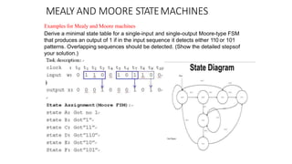
  • 60. MEALY AND MOORE STATEMACHINES Examples for Mealy and Moore machines Derive a minimal state table for a single-input and single-output Moore-type FSM that produces an output of 1 if in the input sequence it detects either 110 or 101 patterns. Overlapping sequences should be detected. (Show the detailed stepsof your solution.)
  • 62. MEALY AND MOORE STATEMACHINES StateAssignment (Mealy FSM): stateA: Got no 1 state B: Got‖1‖ state C: Got‖11‖ state D: Got‖10” Sate Table (Mealy FSM)
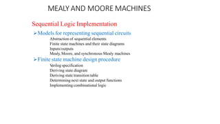
  • 63. MEALY AND MOORE MACHINES Sequential Logic Implementation Models for representing sequential circuits Abstraction of sequential elements Finite state machines and their state diagrams Inputs/outputs Mealy, Moore, and synchronous Mealy machines Finite state machine design procedure V erilog specification Deriving state diagram Deriving state transition table Determining next state and output functions Implementing combinational logic
  • 64. MEALY AND MOORE MACHINES Mealy vs. Moore Machines Moore: outputs depend on current state only Mealy: outputs depend on current state and inputs Ant brain is a Moore Machine (Output does not react immediately to input change) Wecould have specified a Mealy FSM (Outputs have immediate reaction to inputs .As inputs change, so does next state, doesn’t commit until clocking event) Specifying Outputs for a Moore Machine Output is only function of state. Specify in state bubble in state diagram. Example: sequence detector for 01 or 10
  • 65. MEALY AND MOORE MACHINES Specifying Outputs for a Mealy Machine Output is function of state and inputs .Specify output on transition arc between states. Example: sequence detector for 01 or 10
  • 66. MEALY AND MOORE MACHINES Comparison of Mealy and Moore Machines Mealy Machines tend to have less states Different outputs on arcs (n^2) rather than states (n) Moore Machines are safer to use Outputs change at clock edge (always one cycle later) In Mealy machines, input change can cause output change as soon as logic is done – a big problem when two machines are interconnected – asynchronous feedback Mealy Machines react faster to inputs React in same cycle – don't need to wait for clock In Moore machines, more logic may be necessary to decode state into outputs – more gate delays after
  • 67. SYNCHRONOUSAND ASYNCHRONOUS SEQUENTIAL CIRCUITS synchronous sequential circuits a clock signal consisting of pulses, controls the state variables which are represented by flip-flops. they are said to operatein pulse mode. asynchronous circuits state changes are not triggered by clock pulses. they depend on the values of the input and feedback variables. two conditions for proper operation: 1.-inputs to the circuit must change one at a time and must remain constant until the circuit reaches stable state. 2.-feedback variables should change also one at a time. when all internal signals stop changing, then the circuit is said to have reached stable state when the inputs satisfy condition 1 above, then the circuit is said to operate in fundamental mode. Analysis of Clocked Sequential Circuits The analysis of a sequential circuit consists of obtaining a table or a diagram for the time sequence of inputs, outputs, and internal states. It is also possible to write Boolean expressions that describe the behavior of the sequential circuit. These expressions must include the necessary time sequence, either directly or indirectly.
  • 68. SYNCHRONOUS AND ASYNCHRONOUS SEQUENTIAL CIRCUITS State Equations The behavior of a clocked sequential circuit can be described algebraically by means of state equations. A state equation specifies the next state as a function of the present state and inputs. Consider the sequential circuit shown in Fig. 5-15. It consists of two D flip-flops A and B, an input x and an output y. State equation A(t+1) =A(t) x(t) + B(t) x(t) B(t+1) =A`(t) x(t) A state equation is an algebraic expression that specifies the condition for a flip-flop state transition. The left side of the equation with (t+1) denotes the next state of the flip-flop one clock edge later. The right side of the equation is Boolean expression that specifies the present state and input conditions that make the next state equal to 1. Y(t) = (A(t) + B(t)) x(t)`
  • 69. SYNCHRONOUS AND ASYNCHRONOUS SEQUENTIAL CIRCUITS State Table The time sequence of inputs, outputs, and flip-flop states can be enumerated in a state table (sometimes called transition table). State Diagram 1/0 : means input=1 output=0 The information available in a state table can be represented graphically in the form of a state diagram. In this type of diagram, a state is represented by a circle, and the transitions between states are indicated by directed lines connecting the circles.
  • 70. SYNCHRONOUS AND ASYNCHRONOUS SEQUENTIAL CIRCUITS Flip-Flop Input Equations The part of the combinational circuit that generates external outputs is descirbed algebraically by a set of Boolean functions called output equations. The part of the circuit that generates the inputs to flip-flops is described algebraically by a set of Boolean functions called flip-flop input equations. The sequential circuit of Fig. 5-15 consists of two D flip-flops A and B, an input x, and an output y. The logic diagram of the circuit can be expressed algebraically with two flip-flop input equations and an output equation: DA=Ax + Bx,DB =A`x and y = (A+B)x` Analysis with D Flip-Flop The circuit we want to analyze is described by the input equation The DA symbol implies a D flip-flop with output A. The x and y variables are the inputs to the circuit. No output equations are given, so the output is implied to come from the output of the flip-flop.
  • 71. SYNCHRONOUS AND ASYNCHRONOUS SEQUENTIAL CIRCUITS The binary numbers under A y are listed from 000 through 111 as shown in Fig. 5-17(b). The next state values are obtained from the state equation The state diagram consists of two circles-one for each state as shown in Fig.5-17(c)
  • 72. SYNCHRONOUS AND ASYNCHRONOUS SEQUENTIAL CIRCUITS ASYNCHRONOUS SEQUENTIAL CIRCUIT Analysis of asynchronous circuits Procedure: – Cut all feedback paths and insert a delay element at each point where cut was made – Input to the delay element is the next state variable yi while the output is the present value yi . – Derive the next-sate and output expressions from the circuit – Derive the excitation table – Derive the flow table – Derive a state-diagram from the flow table – Asynchronous circuits don’t use clock pulses • State transitions by changes in inputs – Storage Elements: • Clock less storage elements or Delay elements – In many cases, as combinational feedback • Normally much harder to design
  • 73. SYNCHRONOUS AND ASYNCHRONOUS SEQUENTIAL CIRCUITS yi = Yi in steady state (but may be different during transition) Simultaneous change in two (or more) inputs is prohibited. The time between two changes must beless than the time of stability. Analysis
  • 74. SYNCHRONOUS AND ASYNCHRONOUS SEQUENTIAL CIRCUITS 3.Draw a map by using rows: yi’s, columns: inputs, entries: Yi’s 4.Tohave a stable state, Y must be = y (circled) (Transition T able) Y1 Y2 At y1y2x = 000, if x: 0  1 thenY1Y2: 00  01 then y1y2 = 01 (2nd row):stable
  • 75. SYNCHRONOUS AND ASYNCHRONOUS SEQUENTIAL CIRCUITS In general, if an input takes the circuit to an unstable state, yi’s change untila stable State TableAs synchronous state is found. General state of circuit: y1y2x: There are 4 stable states: 000, 011, 110, 101 and 4 unstable states. Flow Table As Transition Table (but with symbolic states): SYNTHESIS OFASYNCHROUNOUS CIRCUITS This topic is not covered in this course. it belongs to a more advanced logic design course.This it is very important in todays digital systems design because clocks are so fast that they present propagation delays making subsystems to operate out of synchronization. Techniques for synthesis of asynchronous circuits include The hoffman or classic synthesis approach Handshaking signaling for two subsystems to communicate asynchronously
  • 76. SHIFT REGISTERS Introduction : Shift registers are a type of sequential logic circuit, mainly for storage of digital data. They are a group of flip-flops connected in a chain so that the output from one flip-flop becomes the input of the next flip-flop. Most of the registers possess no characteristic internal sequence of states. All the flip-flops are driven by a common clock, and all are set or reset simultaneously. Shift registers are divided into two types. 1. Uni directional shift registers 1.Serial in – serial out shift register 2.Serial in – parallel out shift register 3.Parallel in – serial out shift register 4. Parallel in – parallel out shift register 2. Bidirectional shift registers 1.Left shift register 2. Right shift register
  • 77. SHIFT REGISTERS 1.Serial in – serial out shift register A basic four-bit shift register can be constructed using four D flip-flops, as shown below. The operation of the circuit is as follows. The register is first cleared, forcing all four outputs to zero. The input data is then applied sequentially to the D input of the first flip-flop on the left (FF0). During each clock pulse, one bit is transmitted from left to right. Assume a data word to be 1001. The least significant bit of the data has to be shifted through the register from FF0 to FF3. In order to get the data out of the register, they must be shifted out serially. This can be done destructively or non-destructively. For destructive readout, the original data is lost and at the end of the read cycle, all flip-flops are reset to zero.
  • 78. SHIFT REGISTERS Toavoid the loss of data, an arrangement for a non-destructive reading can be done by adding twoAND gates, an OR gate and an inverter to the system. The construction of this circuit is shown below The data is loaded to the register when the control line is HIGH (ie WRITE). The data can be shifted out of the register when the control line is LOW (ie READ). This is shown in the animation below.
  • 79. SHIFT REGISTERS 2.Serial in – parallel out shift register The difference is the way in which the data bits are taken out of the register. Once the data are stored, each bit appears on its respective output line, and all bits are available simultaneously. In the animation below, we can see how the four-bit binary number 1001 is shifted to the Q outputs of the register.
  • 80. SHIFT REGISTERS 3.Parallel in – serial out shift register Afour-bit parallel in - serial out shift register is shown below. The circuit uses D flip-flops and NAND gates for entering data (ie writing) to the register. D0, D1, D2 and D3 are the parallel inputs, where D0 is the most significant bit and D3 is the least significant bit. Towrite data in, the mode control line is taken to LOW and the data is clocked in. The data can be shifted when the mode control line is HIGH as SHIFT is active high. The register performs right shift operation on the application of a clock pulse, as shown in the animation below.
  • 81. SHIFT REGISTERS 4.Parallel in –parallel out shift register For parallel in - parallel out shift registers, all data bits appear on the parallel outputs immediately following the simultaneous entry of the data bits. The following circuit is a four-bit parallel in - parallel out shift register constructed by D flip-flops. The D's are the parallel inputs and the Q's are the parallel outputs. Once the registeris clocked, all the data at the D inputs appear at the corresponding Q outputs simultaneously.
  • 82. SHIFT REGISTERS AND COUNTERS Bidirectional Shift Registers The registers discussed so far involved only right shift operations. Each right shift operation has the effect of successively dividing the binary number by two. If the operation is reversed (left shift), this has the effect of multiplying the number by two. With suitable gating arrangement a serial shift register can perform both operations. A bidirectional, or reversible, shift register is one in which the data can be shift either left or right. A four-bit bidirectional shift register using D flip-flops is shown below Here a set of NAND gates are configured as OR gates to select data inputs from the right or left adjacent bitable, as selected by the LEFT/RIGHT control line. The animation below performs right shift four times, then left shift four times. Notice the order of the four output bits are not the same as the order of the original four input bits.
  • 83. SHIFT REGISTERS AND COUNTERS COUNTERS Two of the most common types of shift register counters are introduced here: the Ring counter and the Johnson counter. They are basically shift registers with the serial outputs connected back to the serial inputs in order to produce particular sequences. These registers are classified as counters because they exhibit a specified sequence of states. Ring Counters A ring counter is basically a circulating shift register in which the output of the most significant stage is fed back to the input of the least significant stage. The following is a 4-bit ring counter constructed from D flip-flops. The output of each stage is shifted into the next stage on the positive edge of a clock pulse. If the CLEAR signal is high, all the flip-flops except the first one FF0 are reset to 0. FF0 is preset to 1 instead.
  • 84. SHIFT REGISTERS AND COUNTERS Since the count sequence has 4 distinct states, the counter can be considered as a mod-4 counter. Only 4 of the maximum 16 states are used, making ring counters very inefficient in terms of state usage. But the major advantage of a ring counter over a binary counter is that it is self-decoding. No extra decoding circuit is needed to determine what state the counter is in.
  • 85. SHIFT REGISTERS AND COUNTERS Johnson Counters Johnson counters are a variation of standard ring counters, with the inverted output of the last stage fed back to the input of the first stage. They are also known as twisted ring counters. An n- stage Johnson counter yields a count sequence of length 2n, so it may be considered to be a mod- 2n counter. The circuit above shows a 4-bit Johnson counter. The state sequence for the counter is given in the table as well as the animation on the left. Again, the apparent disadvantage of this counter is that the maximum available states are not fully utilized. Only eight of the sixteen states are being used. Beware that for both the Ring and the Johnson counter must initially be forced into a valid state in the count sequence because they operate on a subset of the available number of states. Otherwise, the ideal sequence will not be followed.