SlideShare a Scribd company logo
VLSI Design Flow
Very-large-scale integration is the process of creating an integrated circuit
by combining millions or billions of MOS transistors onto a single chip.
VLSI began in the 1970s when MOS integrated circuit chips were developed
and then widely adopted, enabling complex semiconductor and
telecommunication technologies.
The “Y chart” in VLSI (Very Large Scale Integration) refers to a graphical
representation that illustrates the interrelation between the design,
fabrication, and test processes in semiconductor manufacturing. It is called
the “Y chart” because of its shape, which resembles the letter “Y”
Steps in RTL to GDSII Flow
RTL - Register Transfer level
GDSII - Graphic Design System II
The RTL to GDSII flow is a process in VLSI design that converts an RTL
description of a digital circuit into a physical layout ready for fabrication. It
involves stages like RTL synthesis, floor planning, placement, routing, and
ultimately generating the GDSII file format, which contains the layout data.
This meticulous process ensures the final IC layout accurately reflects the
desired functionality and meets fabrication requirements
Design Specifications
The first step in VLSI design involves defining specifications, which outline
requirements for functionality, performance, power consumption, area
constraints, technology node, interfaces, reliability, and cost targets. These
specifications guide the design process, ensuring that the resulting
integrated circuit meets the desired criteria and fulfills its intended purpose
effectively and efficiently.
Logic Design / Functional Verification
RTL (Register Transfer Level) design involves describing digital circuits at a
level where data is transferred between registers. Functional verification
ensures that the RTL design behaves as intended. Simulations, primarily
used for verification, involve test benches with stimuli and expected
responses. RTL is specified in either of the following languages.
RTL Synthesis
RTL synthesis is a key stage in VLSI design where RTL descriptions of digital
circuits are converted into gate-level netlists. This involves mapping RTL
constructs to logic gates and flip-flops from a technology library while
optimizing for area, timing, and power. The output is a gate-level netlist
used for subsequent design stages like physical design and verification.
Convertes RTL to a circuit out of components from the Standard cell
Library(SCL).
Standard Cell: Standard cells are pre-designed components used in VLSI
design to build digital integrated circuits efficiently. They come in libraries
containing various logic functions like AND, OR, and flip-flops. Each cell is
characterized by its performance, power, and area metrics. Designers use
these cells as building blocks to create custom digital circuits.
Standard cells are of different sizes and may be same cells is of different
sizes and properties.
Floorplanning & Powerplanning
Floorplanning: Floorplanning involves determining the locations, shape,
size of modules in a chip and as such it estimates the chip area, delay and
the wiring congestion, thereby providing a ground work for layout.
Partitining is one of the process which plays a key role before
floorplanning. Design partitioning is the practice of dividing a system on
chip (SoC) into small blocks. This allows you to efficiently manage
semiconductor designs as a related set of functional blocks.
It is importat to note that the partitioning should be done in such a way that
the intrconnections between the partitioned blocks should be minimum.
Partitioning and Floor Planning are two of the design processes in the VLSI
design and are used to reduce the size of the circuit. Floorplanning includes
partition of chip die into different system blocks and also I/O pads.
Every module has been assigned an appropriate area and aspect ratio.
Every pin of the module has connection with other modules or periphery
of the chip.
Modules are arranged in a way such that it consumes lesser area on a chip.
Power Planning : Power planning is a sub-step of floor planning in a
physical design flow. In this step we route the VDD & VSS, usually as a mesh
grid in order to equally supply the power across design by reducing the IR-
drop due to the metal resistance.
During power planning, the VDD and VSS rails also have to be
defined. Objective of power planning is to meet It involves the distribution
of power supplies and design of power distribution networks(PDN) to
ensure stable and reliable power delivery to all components. Power
planning involves- calculating number of power pins required, number of
rings and straps, width of rings and straps and IR drop. These are placed on
the upper metal layers, as these have to be thicker than the lower metal
layers, to have low resistance.
Power planning includes performing power integrity analysis to ensure that
the voltage levels across the chip remain within specified tolerances under
varying operating conditions.
There are different types types of floorplannings which involves different
pre-designed functional blocks.Her we are going to learn about two types of
which includes the placement of pre-designed functional blocks.
Macro Planning or Macro Placement:
Macro planning allows you to determine how much shelf space each of your
product groups should get and how the space should be divided up
according to the overall sales contribution and importance.
Macros: Macros are predefined functional blocks with specific
functionalities, such as processors, memory arrays, I/O interfaces. Macros
are typically designed and verified independently and are then integrated
into the chip design as reusable components.
During macro placement, designers make strategic decisions regarding the
placement of macros based on various factors including functional
hierarchy, connectivity, power and signal integrity considerations, and
physical design constraints.
IP integration or IP block placement:
The floorplanning of IPs (Intellectual Properties) is commonly referred to
as "IP integration" or "IP block placement" in the context of VLSI (Very
Large Scale Integration) design. This process involves organizing and
positioning IP cores within the chip's silicon die to optimize chip layout,
signal routing, power distribution, and other design considerations.
IP’s: These are pre-designed and pre-verified functional units or modules
that serve specific purposes within an integrated circuit (IC) or chip design.
Semiconductor IP cores are essential building blocks used by chip
designers to accelerate the development process, reduce design complexity,
and achieve faster time-to-market for new semiconductor products.
Semiconductor IPs can include various types of functional blocks, such as
Processor cores, memory cores, interface controllers etc.
IP’s are also called as Preplaced cells. Automated placement and routing
tools places the remaining logical cells in the design onto chip.
This floorplanning should follow certain rules to maintain signal integrity
and meet timing requirements.
Differences between Macros & IP’s :
Macros and IPs serve as reusable functional blocks in VLSI design, yet they
differ in ownership, licensing, design processes, customization options, and
market availability. Macros are internally developed and owned by the
designing company, tailored to specific chip requirements, and not typically
licensed externally. IPs, on the other hand, are commercially available from
IP vendors, undergoing rigorous design and verification processes, and are
licensable for integration into multiple projects. While macros can be
customized to some extent, IPs often offer more configurable options.
Despite similarities in functionality, their distinctions lie in their origin,
accessibility, and flexibility within the chip design ecosystem.
Concepts of Floorplanning :
In VLSI design, floorplanning is a critical early-stage process that involves
the arrangement of functional blocks and components within the chip area,
known as the die.
Die : The term "die" typically refers to the individual unit of a
semiconductor wafer that contains the integrated circuit (IC) or chip.
Core : A "core" typically refers to a fundamental processing unit or
functional block within an integrated circuit (IC) or system-on-chip (SoC).
Cores are designed to perform specific tasks or functions and are often
modular, reusable components that can be integrated into larger designs.
In VLSI design, core and die dimensions adhere to strict rules ensuring
optimal functionality and manufacturability. These rules cover aspects like
aspect ratio constraints, minimum dimensions, spacing rules, alignment
guidelines, clearance requirements, power distribution, routing channels,
and thermal management. Compliance with these rules guarantees efficient
chip performance and reliability
Utilization rate:It is the ratio of the total cell area (for hard macros and
standard cells or soft macro cells) to the core area.
Aspect ratio: Aspect ratio will decide the size and shape of the chip. It
is the ratio between horizontal routing resources to vertical routing
resources (or) ratio of height and width.
Aspect ratio is a critical parameter in semiconductor manufacturing as it
affects various aspects of the fabrication process, including lithography,
etching, and dopant diffusion. Designers often optimize aspect ratios to
meet performance, power and manufacturability requirements in
integrated circuit designs.
The following example, the utilization rate is 100% that is the chip is
completely used by the functional blocks and the aspect ratio is 1
representing the shape of the die as square.
In the following example, the Utilization rate is 50% indicating that the half
of the part of the die area is occupied by the functional blocks or macros or
IP’s. And the aspect ratio is 0.5 representing a rectangle shape.
Concepts of PowerPlanning:
Decoupling Capacitance: Decoupling capacitors are strategically placed
within the power distribution network of a VLSI chip to ensure stable and
reliable operation. They help mitigate voltage fluctuations caused by
sudden changes in current demand, thereby improving noise immunity and
reducing the risk of functional failures.
One of the primary functions of decoupling capacitors is to regulate the
local voltage levels within the chip. They act as charge reservoirs, supplying
additional current to the circuits during transient events, such as switching
activities or clock edges, to maintain stable voltage levels. As these
decoupling capacitors are of hge size and they are highy charged, they can
maintain a constant voltage levels for a long time.
Decoupling capacitors absorb high-frequency noise generated by switching
activities in digital circuits. By providing a low-impedance path to ground,
they effectively filter out noise from the power supply lines, preventing it
from propagating to other parts of the chip and causing interference or
signal integrity issues
Decoupling capacitors plays a crucial role in noise filtering, transient
response, resonance supression and Placement optimization.
Following shows the powerplanning on a die forming a grid to maintain
signal integrity to every functional block.
Placement
In VLSI design, "placement" refers to the process of determining the
physical locations of various components, such as logic gates, flip-flops, and
other circuit elements, on the silicon die. This placement phase occurs after
the logical design phase where the functionality of the circuit is defined.
Minimizing the total wire length is a primary objective during placement.
Shorter interconnects lead to reduced signal delays and power
consumption. Placement algorithms aim to place related components close
to each other to minimize wire length.
Congestion occurs when certain regions of the chip become densely
packed, leading to routing difficulties and potential timing violations.
Effective placement algorithms employ congestion-aware techniques to
evenly distribute components and alleviate congestion hotspots.
Proper spacing and alignment of cells are essential to ensure
manufacturability and reliability. Placement algorithms enforce spacing
rules to prevent design rule violations and optimize chip manufacturability.
There are mainly two types of Placement methodologies.
- Global Placement
- Detailed Placement
Global Placement: Global placement, also known as coarse placement or
floorplanning, focuses on allocating large functional blocks or macros to
specific regions of the chip. It establishes a high-level floorplan that defines
the approximate placement of major components, such as processor cores,
memory arrays, and I/O pads. Global placement helps set the overall chip
organization and layout constraints before detailed placement
Detailed placement: Detailed placement, also referred to as fine
placement, involves refining the positions of individual cells or standard
cells within each functional block or macro. Detailed placement algorithms
optimize the placement of cells to minimize wirelength, reduce congestion,
and meet timing constraints. This stage of placement requires considering
detailed routing considerations and physical design rules.
For Plaecement, all Standard cells are present in library.
Library: A "Library" typically refers to a collection of standard cell layouts,
each representing a specific logic function or gate. These standard cells are
pre-designed and characterized for various performance metrics such as
timing, power, area, and signal integrity.
During placement, designers choose appropriate standard cells from the
library to implement the desired functionality of the circu uj7it. The library
contains a variety of cells, ranging from basic logic gates (such as NAND,
NOR, AND, OR gates) to more complex functional units (such as flip-flops,
multiplexers, adders, etc.)
In library, there may be same types of standard cells of different driving
capabilities based on the size of the standard cells. As the size increases,
resistance decreases and the driving capability increases.
For example, consider the following netlist, with various logic elements.
Let’s take the Standard cells from the library for the elements of above
netlist.
After the placement we need some placement optimization to make sure
that the design is should meet the timing requirement and should not not
include any timing violations. The design after placement is as follows:
In the process of placement, some of the inter connnections between the
functional blocks will a much larger delay and because of this signal quality
may degrade and results in increase of the signal transition delay.
To solve this issue an do maintain the signal quality from the data path
source to the destination we place buffers in between them.
Buffers are often used to improve signal quality and reduce delay in the
transmission of signals. A buffer is a logic gate that receives an input signal
and re-transmits it with minimal delay and minimal distortion.
As we know, the basic property of buffer is to maintain the input and output
through it, same to same without any signal distortion. So buffers are the
important part of the placement, to maintain the signal quality.
Below is the example, to show the use of buffers in longer delay paths.
In this way, we can optimize the Placement upto a large extent.
Clock Tree Synthesis
Clock tree synthesis (CTS) is a crucial step in the design of digital integrated
circuits (ICs), particularly in very large scale integration (VLSI) design. It
involves the generation of a network of clock distribution lines throughout
the chip to ensure that the clock signal reaches all sequential elements (like
flip-flops) synchronously and with minimum skew.
It ensures the building of Clock tree in such a way that the clock signal will
have a same delay or latency time for every functional block to travel from
clock source to clock destination at the functional blocks.
Not only
considering about maintaining the same delay for proper working of the
circuit, we also have to consider the signal quality. And to maintain the
signal integrity, we will place buffers. While building a clock Tree with
buffers, we have to follow certain rules, like considering the wire length to
place buffers at a distance from other buffers.
There are different in which we can build a Clock Tree to maintain Signal
quality with proper timing requirements.
Various optimization techniques are applied to the clock tree to further
reduce skew and delay. This may involve adjusting the placement and sizing
of buffers, optimizing routing paths, and adjusting the clock tree topology.
There are different ways to build Clock trees, some of them are as
follows:
In clock tree synthesis (CTS), the formation of coupling capacitance is a
significant consideration as it can impact the performance and reliability of
the clock distribution network. Coupling capacitance arises primarily due
to the proximity of signal traces (such as clock lines) to each other on the
chip and can lead to undesirable effects such as clock skew, signal integrity
issues, and increased power consumption. If any logic is transmitted
through a net that affects another neighbouring net due to capacitive
coupling is known as crosstalk.
It depends on coupling capacitance between two neighbouring nets, greater
the coupling capacitance greater will be the crosstalk. It is an undesirable
effect. Coupling capacitance can introduce skew in the clock signals, where
different parts of the clock network experience varying delays. This skew
can lead to timing violations and impact the overall performance of the
chip.
So to improve the clock tree Synthesis without formation of any decoupling
capacitance, we have to maintain certain distance between clock lines.
If we follow such rules, there is no formation of Coupling capacitance
between to parallel clock lines, and it results in a proper clock tree
formation.
And there is another disadvantage of placing the parallel clock lines nearer
to each other known as delta delay.
In clock tree synthesis (CTS), delta delay refers to the difference in delay
experienced by various paths of the clock tree. It's an important parameter
to consider because it directly affects the skew, which is the variation in
arrival times of the clock signal at different points in the chip. Minimizing
delta delay helps ensure that the clock signal reaches all sequential
elements (e.g., flip-flops) synchronously, meeting timing requirements and
reducing the likelihood of timing violations.
Modern CTS tools employ sophisticated algorithms to optimize the clock
tree structure and minimize delta delay. These algorithms consider factors
such as buffer placement, wire routing, and timing constraints to achieve
balanced and efficient clock distribution.
To make ensure that there is no formation of Decoupling capacitance and
there is no effect of delta delay in clock tree synthesis, one of the effective
technique known is clock net shielding.
VDD and VSS lines protect the clock signal from coupling and to prevent
delta delay.
In clock net shielding, the clock signal is shielded by the vdd and vss signal
lines that is power and ground lines. The purpose to shield the high speed
clock signal is to protect the data paths and clock signals from radiated
noise and radiated emissions.
After the process of clock net shielding, the layout we can see is as follows:
Power Aware CTS:
Power-aware Clock Tree Synthesis (CTS) is a technique used in VLSI design
to optimize clock distribution networks while considering power
consumption as a key design metric. Traditional CTS focuses primarily on
minimizing clock skew and improving timing characteristics, but power-
aware CTS extends this by also addressing power-related issues.
In power-aware CTS, the goal is to design a clock tree that not only meets
timing requirements but also minimizes power consumption.
We know that, to maintain the signal integrity, we insert buffers in the Clock
tree synthesis.
In Clock Tree Synthesis (CTS), ensuring balanced loading across the clock
tree is fundamental for achieving optimal timing and power characteristics
in VLSI designs. The principle of balancing the load at each node and
employing identical buffers at each level of the tree serves to maintain
consistent signal integrity and minimize skew.
Balanced loading ensures that clock signals experience uniform
propagation delays as they traverse the tree structure. This balance is
essential for meeting setup and hold time requirements across all flip-flops
in the design. When every node drives the same load, it helps prevent
timing violations by ensuring that clock edges arrive at each flip-flop
simultaneously or within the specified timing window.
Delay Tables:
In Clock Tree Synthesis (CTS), Delay Tables are essential data structures
used to characterize the propagation delay of buffers or inverters utilized in
the clock tree. These tables provide detailed information about the delay
introduced by each buffer or inverter under various operating conditions,
such as input slew rates, output loads, and temperature variations.
Delay Tables typically consist of a set of delay values corresponding to
different input slew rates and output loads. These values are obtained
through pre-characterization or simulation of the buffers/inverters under
various conditions. Each entry in the table corresponds to the delay
introduced by the buffer or inverter for a specific combination of input slew
rate and output load. Let us consider the following example
By considering the above values and above circuit, consider the delay tables
as below:
From these Delay tables, we can get the properties of buffers, the capacitive
loads, and the delay of the buffers based of the different skew values and
output capacitive loads.
Static Timing Analysis
Static timing analysis (STA) is a critical step in the design and verification of
integrated circuits (ICs), particularly in the realm of Very Large-Scale
Integration (VLSI) design. STA involves evaluating the timing behavior of
digital circuits to ensure that they meet timing requirements specified by
the designer.
One of the primary objectives of STA is to determine whether the design
satisfies setup and hold time constraints for all sequential elements, such as
flip-flops or latches, under all possible operating conditions. STA analyzes
the timing paths within the design, considering factors such as signal
propagation delays, clock skew, and clock uncertainties. By examining these
timing paths, STA identifies critical paths with the longest delay, which
dictate the maximum achievable clock frequency of the design.
STA tools use delay information, typically derived from delay tables or delay
models, to perform timing analysis accurately. The results of STA provide
designers with insights into the timing performance of their designs,
guiding optimization efforts to meet timing constraints and achieve desired
performance goals.
If there is any violation in the timing or the design doesn’t meet the timing
specifications, we have to redesign, resynthesize and modify timing
constraints to meet the desired timed requirements.
Let’s see some of the timing related terminologies and rules of Static Timing
Analysis.
Launch Flop & Capture Flop:
Launch Flop: A "launch flop" is a flip-flop or latch used to launch a signal or
data into a synchronous digital circuit. It is typically associated with the
beginning of a timing path. The launch flop receives the data input that
needs to be propagated through the digital circuit.
Capture Flop: A "capture flop" is a flip-flop or latch used to capture a signal
or data at a specific point in a synchronous digital circuit. It is typically
associated with the end of a timing path. Upon receiving the clock signal,
the capture flop samples and captures the data input at the specific point in
time defined by the clock edge
Latency time: It is the time taken by the clock signal to travel from the
clock source to the destination at the flip flop or It is the arrrival time of a
clock signal to flip flop.
Source Latency: "Source latency" typically refers to the delay or latency
introduced by a source component in a system or process. The source
component could be a hardware device, software module, or any other
entity responsible for generating data, signals, or events.
Network latency: Network latency refers to the time delay that occurs when
data packets travel from their source to their destination over a computer
network. It is a measure of the time it takes for data to traverse the network
between two points and is typically measured in milliseconds (ms) or
microseconds (µs).
Clock Skew:Clock skew refers to the difference in arrival times of a clock
signal at different elements or components of a synchronous digital circuit.
Slew:"slew" refers to the rate of change of a signal transition, typically
measured as the time it takes for a signal to transition between two logic
levels (e.g., from low to high or high to low). It represents how quickly the
voltage level of a signal changes over time.
Slew rate is usually expressed in terms of voltage change per unit of time,
such as volts per nanosecond (V/ns). A high slew rate indicates a fast
transition, while a low slew rate indicates a slower transition.
Let’s understand the difference between Fast Slew and Slow Slew.
Jitter: Jitter is the
variation of the
clock period from edge to edge It is essentially the deviation from the
expected or desired timing of signal events. Jitter can occur in both periodic
and aperiodic signals.
Clock Uncertainity: Clock uncertainty, also known as clock skew
uncertainty or clock timing uncertainty, refers to the variation or
uncertainty in the arrival times of clock signals at different components or
elements of a digital circuit. It represents the amount of deviation from the
ideal arrival times of clock edges specified by the clock period
Propagation delay: Propagation delay refers to the time taken for a signal
to travel from its source to its destination in a digital circuit. It represents
the time delay incurred as a signal propagates through various components
of the circuit, such as logic gates, wires, and interconnects
Path delay: Path delay, refers to the total time taken for a signal to
propagate through a specific path in a digital circuit. It represents the
cumulative delay incurred as the signal traverses through various logic
gates, interconnects, and other components along the path.
Clock-to-Q Delay : The delay associated with the capture of data at flip-
flops or latches along the path. This includes the time taken for the output
of a flip-flop or latch to become stable after the arrival of the clock signal.
Fanout: "Fanout" refers to the number of logic gates or other load
components that can be connected to the output of a specific logic gate or
driver without causing performance degradation or violating electrical
specifications.
Let us consider the following example, for the maximum fanout.
Critical path: "Critical path" refers to the longest path through a digital
circuit from input to output, where the cumulative delay along this path
determines the overall timing performance of the circuit. It represents the
path that imposes the most significant constraints on the circuit's
operational speed and determines the maximum achievable clock
frequency.
Let’s see an example of about the Critical Path delay.
False Path : A "False path" refers to a path in a circuit that is not used to
propagate data during normal operation. Despite existing in the design,
signals do not flow along a false path during normal operation, either due to
conditional logic or because the path is never activated.
Multicycle path: A multicycle path, also known as a multicycle constraint,
refers to a timing path in a digital circuit where the data does not need to be
captured or launched on every clock cycle. Instead, the data may be valid
for multiple clock cycles, allowing for a longer timing window for data
capture or launch
Setup time: Setup time refers to the minimum time duration before the
active edge of a clock signal during which the input data signal must remain
stable and unchanged for proper capture by a flip-flop or latch in a
synchronous digital circuit. In simpler terms, it is the time period prior to
the arrival of the clock edge during which the input signal should not
change to ensure reliable data capture by the flip-flop or latch
Hold time : Hold time refers to the minimum duration after the active edge
of a clock signal during which the input data signal must remain stable and
unchanged for proper capture by a flip-flop or latch in a synchronous digital
circuit. In simpler terms, it is the time period following the arrival of the
clock edge during which the input signal should not change to ensure
reliable data capture by the flip-flop or latch.
Slack: "Slack" refers to the amount of time by which a signal can be
delayed without violating timing constraints. A positive slack indicates that
the signal has some margin and can be delayed by that amount without
causing timing violations. Conversely, a negative slack indicates that the
signal is violating timing constraints, and action must be taken to correct
the issue, such as optimizing the circuit or adjusting timing constraints.
Setup Timing Analysis:
The setup timing check can be measured as following for ideal clocks.
The setup timing checked always at the next clock edge.
Here, for setup timing analysis, the total delay i.e, from clk of launch flop to
the capture flop including the combo. Delay must be less than the clock
period
As we know, in real time, the concept of set up time, clock jitter, clock
uncertainty also exists, the timing check for setup can be modified as
By considering the real time context, the total delay i.e, from clk of launch
flop to the capture flop including the combo. Delay must be less than the
clock period by considering the uncertainty and skew.
The equation for setup timing analysis is given as follows:
(Clk-to-Q)+(Combo.) < (Clock Period)–(Clock Skew)–(Clock Uncertainty)
CLK-TO-Q + COMBO < T - S - U
In the above equation, CLK-to-Q + COMBO -----> Data Arrival Time
T - S - U ------> Data Required Time
From the definition, Slack = Data Required Time - Data Arrival Time
If slack is positive, that means there are no timing violation in case of setup
timing check.
If Slack is negative, that means, there is a Setup violation, and we have to
optimize the design to discard the violation.
For real clocks the buffers are also present in the Clock path.
Let’s see an example which considers the setup timing check with real
clocks. While considering the real clocks, the delay of buffers is also
considered as a part of the Clock Time period and as well as in Arrival time.
Hold timing Analysis:
The setup timing check can be measured as following for ideal clocks.
The setup timing checked always at the same clock edge.
Here, for setup timing analysis, the total delay i.e, from clk of launch flop to
the capture flop including the combo. Delay must be less than the Hold
time.
As we know, in real time i.e., for real clocks, the concept of Hold
uncertainty, buffer delays are also considered.
So the timing check for Hold can be modified as..
The equation Hold time analysis is given by,
(Clk-to-Q)+(Combo.) > (Hold Time) + (Hold Uncertainty)
CLK-TO-Q + COMBO > H + HU
In the above equation, CLK-to-Q + COMBO -----> Data Arrival Time
H + HU ------> Data Required Time
From the definition, Slack = Data Arrival Time - Data Required Time
In Static timing Analysis, the Skew is very imporant. In ideal, the design
should be designed in such a way that the Skew must be minimized to Zero.
But in practical case, it is not possible, we have to minimize the Skew nearer
to 0.
Possible ways to improve the Set up violations.
1. Gate sizing and Insertion
2. Clock gating
3. Timing Constraints Optimization
4. Adjust Clock timing
5. Buffer Insertion
6. Optimize timing paths
Possible ways to improve the Hold vioaltion:
1. Clock Gating
2. Library cell replacement
3. Gate sizing
4. Clock tree synthesis
5. Buffer Insertion
ROUTING
Routing in VLSI is making physical connections between signal pins using
metal layers. Following Clock Tree Synthesis (CTS) and optimization, the
routing step determines the exact pathways for interconnecting standard
cells, macros, and I/O pins.
Steps in Routing :
Each metal layer in a grid based routing system has its tracks and preferred
routing direction, which are described in a unified cell in the standard cell
library. Routing activities are divided into four steps:
1. Global Routing
2. Track assignment
3. Detail Routing
4. Search and repair
1. Global Routing: Global route assigns nets to particular metal layers and
global routing cells. The global route aims to avoid crowded global cells
while making as few diversions as possible. Global routes also avoid pre-
routed P/G, placement, and routing bottlenecks.
2. Track Assignment: It allocates each net to a certain track and lays down
actual metal traces. To reduce the number of vias, it attempts to create long,
straight lines. At this stage, physical DRC(Design Rule Check) is not
considered.
3. Detail Routing: Detail routing seeks to repair any DRC violations following
track assignment using a set size small region (Sbox). The detailed routing
goes through the whole design box by box until the routing pass is finished .
It also performs timing driven routing.
4. Search and repair: This resolves any remaining DRC breaches using many
iterative loops with progressively bigger Sbox sizes. DRC rules make sure
that the layout is meeting is following the certain design rules.
Below is the Part of a real chip viewed by an electron microscope (with
artificial colors). In the below diagram, we can see that the wires and pins
are on lower planes connected by vias (light blue)
Let us consider the below layout which had crossed the design steps of
Floorplanning , placement, Clock tree synthesis, Static timing analysis.
There are so many algorithms that are followed in routing process. One of
such algorithm is Lee’s algorithm used in the purpose of Maze routing.
This algorithm is also known as Maze routing Lee’s algorithm. Lee
algorithm searches for the shortest path between two terminals and
guarantees to find a route between two points if the connection exists.
This algorithm represents the routing layer as a grid as shown below
This algorithm will be followed by selecting the adjacent cells of every cell
excepting the diagonal cells. It is shown below.
The process will continue until the destination is reached and then the the
routing happens as shown below.
Now will get the routed layout, and after that, as a part of routing process,
DRC cleaning process will takes place which ensures, whether the layout
follows all specified DRC rules.
There are so many design rules that should be followed as a part of routing
process. Also, there are some typical rules, that should must follow while
routing is going on.
1. Wire width
2. Wire pitch
3. Wire spacing
4. Via width
5. Via spacing
These all are mentioned below:
1. Wire width: In vlsi fabrication, photolithography technique is used to
form the metal connections. This technique used light to make metal
connections.As light have a minimum wavelength, using it, we can make
minimum width of metal connections. It means the optical wavelength of
light can make metal connections.
2. Wire pitch: As per DRC, there is another rule for wire pitch and it should
be maintained ,minimum. We have to optimize the layout, to maintain a
minimum pitch.
3. Wire spacing: The wire spacing between two data paths, or critical
paths, should be maintained and it should not go below the minimum limit.
As we know that if we make interconnections, by violating the minimum
wire pitch rule, it may results in the formation of coupling capacitance, and
may results in crosstalk issues and Signal integrity issues So, it it is
important to maintain a minimum distance. For this kind of problem, it is
not possible, to shield the data path, to prevent it form crosstalk issues. As
net shielding is a difficult task, it is only applicable to critical paths in a
layout, like high speed clock signals or some critical data paths.
4. Via width:(Via – The dip of a whoel between ywo or more metal layers
used to connnect layers.) The DRC rule specify the via width should be
minimum., It can be more, but it can’t be minimum to violate DRC rules.
5. Via spacing:The DRC rule specifies that the minimum spacing between
two vias is maintained. They should be at any maximum distance, but min
distance is maintained, to make ensure the drc is not violated.
-->Major problems in routing arrives when interconects are formed
between the routes, so we have to avoid such DRC violations.
Parasitic Extraction:
After the DRC checking, the next step is parasitic extraction.
Parasitic extraction is a vital process in integrated circuit (IC) design,
focusing on identifying and characterizing unintended electrical effects
known as parasitics. These effects, including resistance, capacitance,
Every net has its own resistance and capacitance, so parasitic extraction
refers to the extraction of these parameters and make ensure whether the
properties doesn’t violate any required parameters in physical design.
Capacitance and Resistance of interconnects, known as nets, significantly
influence the performance and behavior of integrated circuits. Capacitance
directly impacts signal propagation delay along interconnects, contributing
to the RC time constant. Higher capacitance leads to longer delays, affecting
circuit speed. Additionally, high capacitance can cause signal integrity
issues such as distortion, ringing, and crosstalk, potentially compromising
the reliability of the circuit. Furthermore, capacitance between nets results
in dynamic power consumption during charging and discharging cycles.
Resistance also plays a critical role, contributing to the RC time constant
along with capacitance. Increased resistance prolongs signal propagation
delay and can lead to voltage droop, especially in lengthy interconnects or
high-current paths.
Sign off:
Now, There are some other steps as a part of Sign Off process. These are
some verification processes like Design Rule check(DRC) and Layout Vs
Schematic(LVS).
Design Rule Check(DRC) :
Design Rule Checking (DRC) is a pivotal step in the VLSI design workflow,
tasked with verifying that the layout adheres rigorously to the specifications
and constraints dictated by the fabrication technology. At its core, DRC
scrutinizes the geometric aspects of the layout against a predefined set of
rules, encompassing parameters like minimum feature size, spacing, width,
overlap, and alignment. These rules are intricately tied to the specific
fabrication process and technology node being utilized, with
semiconductor foundries furnishing designers with a comprehensive set of
guidelines to ensure manufacturability and yield. DRC operates across
multiple levels of design hierarchy, encompassing cell, block, and chip
levels, to ensure compliance at both component and overall layout levels.
Layout Vs Schematic(LVS) :
Layout vs. Schematic (LVS) verification is an indispensable phase in VLSI
design, ensuring the harmony between the physical layout and its
schematic representation. LVS scrutinizes the geometric layout of
components, such as transistors and interconnects, against the schematic
netlist derived from the design specifications. This comparison serves to
validate the connectivity between nodes in the layout and their
counterparts in the schematic, guaranteeing that electrical connections are
accurately depicted in both representations. Moreover, LVS meticulously
checks device parameters like size, placement, and orientation to confirm
alignment with the schematic's specifications, ensuring consistency in
device sizing and placement.
After all the verifications done, the final step is to send the chip for
fbrication. For that, the GDSII file is sent to fabrication unit to get the chip
manufacture.
GDSII:
A GDSII (Graphical Data System II) file, also known as stream format, is a
standard file format used in the semiconductor industry for exchanging
information related to the layout of integrated circuits. A GDSII file typically
contains the following components:
Structures and Layers: GDSII files store geometric shapes and structures
representing the layout of an integrated circuit. These structures include
polygons, paths, rectangles, circles, and text labels. Each structure is
assigned to a specific layer, which defines its purpose or function within the
layout hierarchy.
Heirarchical Information: GDSII supports hierarchical design, allowing
complex layouts to be organized into a hierarchical structure. Each level of
hierarchy may contain subcells, which can in turn contain additional
subcells, forming a hierarchical tree structure.
Cell References: GDSII files include references to cells or instances placed
within the layout. These references specify the location, orientation, and
scaling of the instances relative to their parent cells
DRC Rules and Parameters: Some GDSII files may include design rule
information, such as minimum feature size, spacing rules, and other
constraints imposed by the semiconductor fabrication process. These rules
help ensure that the layout adheres to the requirements of the
manufacturing technology.

More Related Content

What's hot (20)

PPTX
Define Width and Height of Core and Die (http://www.vlsisystemdesign.com/PD-F...
VLSI SYSTEM Design
 
DOCX
Vlsi interview questions compilation
Rajesh M
 
PDF
Understanding cts log_messages
Mujahid Mohammed
 
ODP
Inputs of physical design
Kishore Sai Addanki
 
PDF
Basic synthesis flow and commands in digital VLSI
Surya Raj
 
PDF
Floorplanning in physical design
Murali Rai
 
PPTX
CAD: Floorplanning
Team-VLSI-ITMU
 
PPTX
ZERO WIRE LOAD MODEL.pptx
VishalYadav29718
 
PPT
Timing and Design Closure in Physical Design Flows
Olivier Coudert
 
PPTX
Eco
Rajesh M
 
PPTX
Vlsi physical design automation on partitioning
Sushil Kundu
 
PPTX
GUI for DRV fix in ICC2
Prashanth Chokkarapu
 
ODP
axi protocol
Azad Mishra
 
PPTX
Synopsys Fusion Compiler-Comprehensive RTL-to-GDSII Implementation System
Mostafa Khamis
 
PDF
Vavo app irdrop_em_analysis_flow
Alan Tran
 
PPTX
2Overview of Primetime.pptx
ShivangPanara
 
PPT
Multiprocessor Systems
vampugani
 
PDF
Implementing Useful Clock Skew Using Skew Groups
M Mei
 
PDF
VLSI-Physical Design- Tool Terminalogy
Murali Rai
 
Define Width and Height of Core and Die (http://www.vlsisystemdesign.com/PD-F...
VLSI SYSTEM Design
 
Vlsi interview questions compilation
Rajesh M
 
Understanding cts log_messages
Mujahid Mohammed
 
Inputs of physical design
Kishore Sai Addanki
 
Basic synthesis flow and commands in digital VLSI
Surya Raj
 
Floorplanning in physical design
Murali Rai
 
CAD: Floorplanning
Team-VLSI-ITMU
 
ZERO WIRE LOAD MODEL.pptx
VishalYadav29718
 
Timing and Design Closure in Physical Design Flows
Olivier Coudert
 
Vlsi physical design automation on partitioning
Sushil Kundu
 
GUI for DRV fix in ICC2
Prashanth Chokkarapu
 
axi protocol
Azad Mishra
 
Synopsys Fusion Compiler-Comprehensive RTL-to-GDSII Implementation System
Mostafa Khamis
 
Vavo app irdrop_em_analysis_flow
Alan Tran
 
2Overview of Primetime.pptx
ShivangPanara
 
Multiprocessor Systems
vampugani
 
Implementing Useful Clock Skew Using Skew Groups
M Mei
 
VLSI-Physical Design- Tool Terminalogy
Murali Rai
 

Similar to VLSI Design Flow - Very Large Scale Integration (20)

PPT
VLSI Design- Guru.ppt
Ram Pavithra Guru
 
PPT
VLSI UNIT-1.1.pdf.ppt
rajukolluri
 
PPT
VLSI Physical Design Automation.ppt
RichikDey5
 
DOC
High bit rate_mul
Sidhu Sidhartha Rai
 
PPT
VLSI unit 1 Technology - S.ppt
indrajeetPatel22
 
PPTX
Vlsi techniques
arpit1010
 
PDF
Digital VLSI Design : Introduction
Usha Mehta
 
DOCX
Report
chetana pareek
 
PPT
Training VLSI Design LAB presentation .ppt
pcjoshi02
 
PDF
Floorplan, Powerplan and Data Setup, Stages
Jason J Pulikkottil
 
PDF
Final Project – RISC V Hard Macros Integration Technology Node: 32nm
cottilard1995
 
PPTX
Module 1 VLSID Design flow - Copy.pptx
ssuserb60e6f
 
PDF
Floorplanning and Powerplanning - Definitions and Notes
Jason J Pulikkottil
 
PDF
Physical Design, ASIC Design, Standard Cells
Jason J Pulikkottil
 
PPT
VLSI- Unit I
MADHUMITHA154
 
PPT
SISTec Microelectronics VLSI design
Dr. Ravi Mishra
 
PPTX
Implementation strategies for digital ics
aroosa khan
 
PDF
Design & Simulation With Verilog
Semi Design
 
PPTX
Vlsi.pptxbbbbbbbbbbbbbbbbbbbbbbbbbbbbbbbbbb
purnimaece321080
 
PPTX
VLSI design flow.pptx
Krishna Kishore
 
VLSI Design- Guru.ppt
Ram Pavithra Guru
 
VLSI UNIT-1.1.pdf.ppt
rajukolluri
 
VLSI Physical Design Automation.ppt
RichikDey5
 
High bit rate_mul
Sidhu Sidhartha Rai
 
VLSI unit 1 Technology - S.ppt
indrajeetPatel22
 
Vlsi techniques
arpit1010
 
Digital VLSI Design : Introduction
Usha Mehta
 
Training VLSI Design LAB presentation .ppt
pcjoshi02
 
Floorplan, Powerplan and Data Setup, Stages
Jason J Pulikkottil
 
Final Project – RISC V Hard Macros Integration Technology Node: 32nm
cottilard1995
 
Module 1 VLSID Design flow - Copy.pptx
ssuserb60e6f
 
Floorplanning and Powerplanning - Definitions and Notes
Jason J Pulikkottil
 
Physical Design, ASIC Design, Standard Cells
Jason J Pulikkottil
 
VLSI- Unit I
MADHUMITHA154
 
SISTec Microelectronics VLSI design
Dr. Ravi Mishra
 
Implementation strategies for digital ics
aroosa khan
 
Design & Simulation With Verilog
Semi Design
 
Vlsi.pptxbbbbbbbbbbbbbbbbbbbbbbbbbbbbbbbbbb
purnimaece321080
 
VLSI design flow.pptx
Krishna Kishore
 
Ad

More from Jason J Pulikkottil (20)

PDF
Unix/Linux Command Reference - File Commands and Shortcuts
Jason J Pulikkottil
 
PDF
Introduction to PERL Programming - Complete Notes
Jason J Pulikkottil
 
PDF
VLSI System Verilog Notes with Coding Examples
Jason J Pulikkottil
 
PDF
Verilog Coding examples of Digital Circuits
Jason J Pulikkottil
 
PDF
Floor Plan, Placement Questions and Answers
Jason J Pulikkottil
 
PDF
Basic Electronics, Digital Electronics, Static Timing Analysis Notes
Jason J Pulikkottil
 
PDF
Floorplanning Power Planning and Placement
Jason J Pulikkottil
 
PDF
Digital Electronics Questions and Answers
Jason J Pulikkottil
 
PDF
Different Types Of Cells, Types of Standard Cells
Jason J Pulikkottil
 
PDF
DFT Rules, set of rules with illustration
Jason J Pulikkottil
 
PDF
Clock Definitions Static Timing Analysis for VLSI Engineers
Jason J Pulikkottil
 
PDF
Basic Synthesis Flow and Commands, Logic Synthesis
Jason J Pulikkottil
 
PDF
ASIC Design Types, Logical Libraries, Optimization
Jason J Pulikkottil
 
PDF
Physical Design Flow - Standard Cells and Special Cells
Jason J Pulikkottil
 
PDF
Physical Design - Import Design Flow Floorplan
Jason J Pulikkottil
 
PDF
Physical Design-Floor Planning Goals And Placement
Jason J Pulikkottil
 
PDF
Short Notes on Verilog and SystemVerilog
Jason J Pulikkottil
 
PDF
VLSI Design Partitioning - Very Large Scale Integration - Practical Problems
Jason J Pulikkottil
 
PDF
Switched Reluctance Motor - Principle Of Operation
Jason J Pulikkottil
 
PDF
Variable Frequency Induction Motor Drives
Jason J Pulikkottil
 
Unix/Linux Command Reference - File Commands and Shortcuts
Jason J Pulikkottil
 
Introduction to PERL Programming - Complete Notes
Jason J Pulikkottil
 
VLSI System Verilog Notes with Coding Examples
Jason J Pulikkottil
 
Verilog Coding examples of Digital Circuits
Jason J Pulikkottil
 
Floor Plan, Placement Questions and Answers
Jason J Pulikkottil
 
Basic Electronics, Digital Electronics, Static Timing Analysis Notes
Jason J Pulikkottil
 
Floorplanning Power Planning and Placement
Jason J Pulikkottil
 
Digital Electronics Questions and Answers
Jason J Pulikkottil
 
Different Types Of Cells, Types of Standard Cells
Jason J Pulikkottil
 
DFT Rules, set of rules with illustration
Jason J Pulikkottil
 
Clock Definitions Static Timing Analysis for VLSI Engineers
Jason J Pulikkottil
 
Basic Synthesis Flow and Commands, Logic Synthesis
Jason J Pulikkottil
 
ASIC Design Types, Logical Libraries, Optimization
Jason J Pulikkottil
 
Physical Design Flow - Standard Cells and Special Cells
Jason J Pulikkottil
 
Physical Design - Import Design Flow Floorplan
Jason J Pulikkottil
 
Physical Design-Floor Planning Goals And Placement
Jason J Pulikkottil
 
Short Notes on Verilog and SystemVerilog
Jason J Pulikkottil
 
VLSI Design Partitioning - Very Large Scale Integration - Practical Problems
Jason J Pulikkottil
 
Switched Reluctance Motor - Principle Of Operation
Jason J Pulikkottil
 
Variable Frequency Induction Motor Drives
Jason J Pulikkottil
 
Ad

Recently uploaded (20)

PPTX
美国电子版毕业证南卡罗莱纳大学上州分校水印成绩单USC学费发票定做学位证书编号怎么查
Taqyea
 
PPT
Carmon_Remote Sensing GIS by Mahesh kumar
DhananjayM6
 
PPTX
Server Side Web Development Unit 1 of Nodejs.pptx
sneha852132
 
PPTX
Day2 B2 Best.pptx
helenjenefa1
 
PPTX
GitOps_Without_K8s_Training_detailed git repository
DanialHabibi2
 
PDF
MAD Unit - 1 Introduction of Android IT Department
JappanMavani
 
PPTX
fatigue in aircraft structures-221113192308-0ad6dc8c.pptx
aviatecofficial
 
PPTX
The Role of Information Technology in Environmental Protectio....pptx
nallamillisriram
 
PPTX
Worm gear strength and wear calculation as per standard VB Bhandari Databook.
shahveer210504
 
PDF
Zilliz Cloud Demo for performance and scale
Zilliz
 
PPTX
265587293-NFPA 101 Life safety code-PPT-1.pptx
chandermwason
 
PPTX
Heart Bleed Bug - A case study (Course: Cryptography and Network Security)
Adri Jovin
 
PPTX
Element 11. ELECTRICITY safety and hazards
merrandomohandas
 
PDF
Ethics and Trustworthy AI in Healthcare – Governing Sensitive Data, Profiling...
AlqualsaDIResearchGr
 
PDF
AI TECHNIQUES FOR IDENTIFYING ALTERATIONS IN THE HUMAN GUT MICROBIOME IN MULT...
vidyalalltv1
 
PDF
Pressure Measurement training for engineers and Technicians
AIESOLUTIONS
 
PPTX
VITEEE 2026 Exam Details , Important Dates
SonaliSingh127098
 
PDF
Introduction to Productivity and Quality
মোঃ ফুরকান উদ্দিন জুয়েল
 
PDF
PORTFOLIO Golam Kibria Khan — architect with a passion for thoughtful design...
MasumKhan59
 
DOC
MRRS Strength and Durability of Concrete
CivilMythili
 
美国电子版毕业证南卡罗莱纳大学上州分校水印成绩单USC学费发票定做学位证书编号怎么查
Taqyea
 
Carmon_Remote Sensing GIS by Mahesh kumar
DhananjayM6
 
Server Side Web Development Unit 1 of Nodejs.pptx
sneha852132
 
Day2 B2 Best.pptx
helenjenefa1
 
GitOps_Without_K8s_Training_detailed git repository
DanialHabibi2
 
MAD Unit - 1 Introduction of Android IT Department
JappanMavani
 
fatigue in aircraft structures-221113192308-0ad6dc8c.pptx
aviatecofficial
 
The Role of Information Technology in Environmental Protectio....pptx
nallamillisriram
 
Worm gear strength and wear calculation as per standard VB Bhandari Databook.
shahveer210504
 
Zilliz Cloud Demo for performance and scale
Zilliz
 
265587293-NFPA 101 Life safety code-PPT-1.pptx
chandermwason
 
Heart Bleed Bug - A case study (Course: Cryptography and Network Security)
Adri Jovin
 
Element 11. ELECTRICITY safety and hazards
merrandomohandas
 
Ethics and Trustworthy AI in Healthcare – Governing Sensitive Data, Profiling...
AlqualsaDIResearchGr
 
AI TECHNIQUES FOR IDENTIFYING ALTERATIONS IN THE HUMAN GUT MICROBIOME IN MULT...
vidyalalltv1
 
Pressure Measurement training for engineers and Technicians
AIESOLUTIONS
 
VITEEE 2026 Exam Details , Important Dates
SonaliSingh127098
 
Introduction to Productivity and Quality
মোঃ ফুরকান উদ্দিন জুয়েল
 
PORTFOLIO Golam Kibria Khan — architect with a passion for thoughtful design...
MasumKhan59
 
MRRS Strength and Durability of Concrete
CivilMythili
 

VLSI Design Flow - Very Large Scale Integration

  • 1. VLSI Design Flow Very-large-scale integration is the process of creating an integrated circuit by combining millions or billions of MOS transistors onto a single chip. VLSI began in the 1970s when MOS integrated circuit chips were developed and then widely adopted, enabling complex semiconductor and telecommunication technologies. The “Y chart” in VLSI (Very Large Scale Integration) refers to a graphical representation that illustrates the interrelation between the design, fabrication, and test processes in semiconductor manufacturing. It is called the “Y chart” because of its shape, which resembles the letter “Y”
  • 2. Steps in RTL to GDSII Flow RTL - Register Transfer level GDSII - Graphic Design System II The RTL to GDSII flow is a process in VLSI design that converts an RTL description of a digital circuit into a physical layout ready for fabrication. It involves stages like RTL synthesis, floor planning, placement, routing, and ultimately generating the GDSII file format, which contains the layout data. This meticulous process ensures the final IC layout accurately reflects the desired functionality and meets fabrication requirements Design Specifications The first step in VLSI design involves defining specifications, which outline requirements for functionality, performance, power consumption, area constraints, technology node, interfaces, reliability, and cost targets. These specifications guide the design process, ensuring that the resulting integrated circuit meets the desired criteria and fulfills its intended purpose effectively and efficiently.
  • 3. Logic Design / Functional Verification RTL (Register Transfer Level) design involves describing digital circuits at a level where data is transferred between registers. Functional verification ensures that the RTL design behaves as intended. Simulations, primarily used for verification, involve test benches with stimuli and expected responses. RTL is specified in either of the following languages. RTL Synthesis RTL synthesis is a key stage in VLSI design where RTL descriptions of digital circuits are converted into gate-level netlists. This involves mapping RTL constructs to logic gates and flip-flops from a technology library while optimizing for area, timing, and power. The output is a gate-level netlist used for subsequent design stages like physical design and verification. Convertes RTL to a circuit out of components from the Standard cell Library(SCL).
  • 4. Standard Cell: Standard cells are pre-designed components used in VLSI design to build digital integrated circuits efficiently. They come in libraries containing various logic functions like AND, OR, and flip-flops. Each cell is characterized by its performance, power, and area metrics. Designers use these cells as building blocks to create custom digital circuits. Standard cells are of different sizes and may be same cells is of different sizes and properties.
  • 5. Floorplanning & Powerplanning Floorplanning: Floorplanning involves determining the locations, shape, size of modules in a chip and as such it estimates the chip area, delay and the wiring congestion, thereby providing a ground work for layout. Partitining is one of the process which plays a key role before floorplanning. Design partitioning is the practice of dividing a system on chip (SoC) into small blocks. This allows you to efficiently manage semiconductor designs as a related set of functional blocks. It is importat to note that the partitioning should be done in such a way that the intrconnections between the partitioned blocks should be minimum. Partitioning and Floor Planning are two of the design processes in the VLSI design and are used to reduce the size of the circuit. Floorplanning includes partition of chip die into different system blocks and also I/O pads.
  • 6. Every module has been assigned an appropriate area and aspect ratio. Every pin of the module has connection with other modules or periphery of the chip. Modules are arranged in a way such that it consumes lesser area on a chip. Power Planning : Power planning is a sub-step of floor planning in a physical design flow. In this step we route the VDD & VSS, usually as a mesh grid in order to equally supply the power across design by reducing the IR- drop due to the metal resistance. During power planning, the VDD and VSS rails also have to be defined. Objective of power planning is to meet It involves the distribution of power supplies and design of power distribution networks(PDN) to ensure stable and reliable power delivery to all components. Power planning involves- calculating number of power pins required, number of rings and straps, width of rings and straps and IR drop. These are placed on the upper metal layers, as these have to be thicker than the lower metal layers, to have low resistance. Power planning includes performing power integrity analysis to ensure that the voltage levels across the chip remain within specified tolerances under varying operating conditions. There are different types types of floorplannings which involves different pre-designed functional blocks.Her we are going to learn about two types of which includes the placement of pre-designed functional blocks.
  • 7. Macro Planning or Macro Placement: Macro planning allows you to determine how much shelf space each of your product groups should get and how the space should be divided up according to the overall sales contribution and importance. Macros: Macros are predefined functional blocks with specific functionalities, such as processors, memory arrays, I/O interfaces. Macros are typically designed and verified independently and are then integrated into the chip design as reusable components. During macro placement, designers make strategic decisions regarding the placement of macros based on various factors including functional hierarchy, connectivity, power and signal integrity considerations, and physical design constraints. IP integration or IP block placement: The floorplanning of IPs (Intellectual Properties) is commonly referred to as "IP integration" or "IP block placement" in the context of VLSI (Very Large Scale Integration) design. This process involves organizing and positioning IP cores within the chip's silicon die to optimize chip layout, signal routing, power distribution, and other design considerations.
  • 8. IP’s: These are pre-designed and pre-verified functional units or modules that serve specific purposes within an integrated circuit (IC) or chip design. Semiconductor IP cores are essential building blocks used by chip designers to accelerate the development process, reduce design complexity, and achieve faster time-to-market for new semiconductor products. Semiconductor IPs can include various types of functional blocks, such as Processor cores, memory cores, interface controllers etc. IP’s are also called as Preplaced cells. Automated placement and routing tools places the remaining logical cells in the design onto chip. This floorplanning should follow certain rules to maintain signal integrity and meet timing requirements.
  • 9. Differences between Macros & IP’s : Macros and IPs serve as reusable functional blocks in VLSI design, yet they differ in ownership, licensing, design processes, customization options, and market availability. Macros are internally developed and owned by the designing company, tailored to specific chip requirements, and not typically licensed externally. IPs, on the other hand, are commercially available from IP vendors, undergoing rigorous design and verification processes, and are licensable for integration into multiple projects. While macros can be customized to some extent, IPs often offer more configurable options. Despite similarities in functionality, their distinctions lie in their origin, accessibility, and flexibility within the chip design ecosystem. Concepts of Floorplanning : In VLSI design, floorplanning is a critical early-stage process that involves the arrangement of functional blocks and components within the chip area, known as the die. Die : The term "die" typically refers to the individual unit of a semiconductor wafer that contains the integrated circuit (IC) or chip.
  • 10. Core : A "core" typically refers to a fundamental processing unit or functional block within an integrated circuit (IC) or system-on-chip (SoC). Cores are designed to perform specific tasks or functions and are often modular, reusable components that can be integrated into larger designs. In VLSI design, core and die dimensions adhere to strict rules ensuring optimal functionality and manufacturability. These rules cover aspects like aspect ratio constraints, minimum dimensions, spacing rules, alignment guidelines, clearance requirements, power distribution, routing channels, and thermal management. Compliance with these rules guarantees efficient chip performance and reliability Utilization rate:It is the ratio of the total cell area (for hard macros and standard cells or soft macro cells) to the core area.
  • 11. Aspect ratio: Aspect ratio will decide the size and shape of the chip. It is the ratio between horizontal routing resources to vertical routing resources (or) ratio of height and width. Aspect ratio is a critical parameter in semiconductor manufacturing as it affects various aspects of the fabrication process, including lithography, etching, and dopant diffusion. Designers often optimize aspect ratios to meet performance, power and manufacturability requirements in integrated circuit designs. The following example, the utilization rate is 100% that is the chip is completely used by the functional blocks and the aspect ratio is 1 representing the shape of the die as square. In the following example, the Utilization rate is 50% indicating that the half of the part of the die area is occupied by the functional blocks or macros or IP’s. And the aspect ratio is 0.5 representing a rectangle shape.
  • 12. Concepts of PowerPlanning: Decoupling Capacitance: Decoupling capacitors are strategically placed within the power distribution network of a VLSI chip to ensure stable and reliable operation. They help mitigate voltage fluctuations caused by sudden changes in current demand, thereby improving noise immunity and reducing the risk of functional failures. One of the primary functions of decoupling capacitors is to regulate the local voltage levels within the chip. They act as charge reservoirs, supplying additional current to the circuits during transient events, such as switching activities or clock edges, to maintain stable voltage levels. As these decoupling capacitors are of hge size and they are highy charged, they can maintain a constant voltage levels for a long time. Decoupling capacitors absorb high-frequency noise generated by switching activities in digital circuits. By providing a low-impedance path to ground, they effectively filter out noise from the power supply lines, preventing it from propagating to other parts of the chip and causing interference or signal integrity issues Decoupling capacitors plays a crucial role in noise filtering, transient response, resonance supression and Placement optimization.
  • 13. Following shows the powerplanning on a die forming a grid to maintain signal integrity to every functional block.
  • 14. Placement In VLSI design, "placement" refers to the process of determining the physical locations of various components, such as logic gates, flip-flops, and other circuit elements, on the silicon die. This placement phase occurs after the logical design phase where the functionality of the circuit is defined. Minimizing the total wire length is a primary objective during placement. Shorter interconnects lead to reduced signal delays and power consumption. Placement algorithms aim to place related components close to each other to minimize wire length. Congestion occurs when certain regions of the chip become densely packed, leading to routing difficulties and potential timing violations. Effective placement algorithms employ congestion-aware techniques to evenly distribute components and alleviate congestion hotspots. Proper spacing and alignment of cells are essential to ensure manufacturability and reliability. Placement algorithms enforce spacing rules to prevent design rule violations and optimize chip manufacturability. There are mainly two types of Placement methodologies. - Global Placement - Detailed Placement Global Placement: Global placement, also known as coarse placement or floorplanning, focuses on allocating large functional blocks or macros to specific regions of the chip. It establishes a high-level floorplan that defines the approximate placement of major components, such as processor cores,
  • 15. memory arrays, and I/O pads. Global placement helps set the overall chip organization and layout constraints before detailed placement Detailed placement: Detailed placement, also referred to as fine placement, involves refining the positions of individual cells or standard cells within each functional block or macro. Detailed placement algorithms optimize the placement of cells to minimize wirelength, reduce congestion, and meet timing constraints. This stage of placement requires considering detailed routing considerations and physical design rules. For Plaecement, all Standard cells are present in library. Library: A "Library" typically refers to a collection of standard cell layouts, each representing a specific logic function or gate. These standard cells are pre-designed and characterized for various performance metrics such as timing, power, area, and signal integrity.
  • 16. During placement, designers choose appropriate standard cells from the library to implement the desired functionality of the circu uj7it. The library contains a variety of cells, ranging from basic logic gates (such as NAND, NOR, AND, OR gates) to more complex functional units (such as flip-flops, multiplexers, adders, etc.) In library, there may be same types of standard cells of different driving capabilities based on the size of the standard cells. As the size increases, resistance decreases and the driving capability increases.
  • 17. For example, consider the following netlist, with various logic elements. Let’s take the Standard cells from the library for the elements of above netlist. After the placement we need some placement optimization to make sure that the design is should meet the timing requirement and should not not include any timing violations. The design after placement is as follows:
  • 18. In the process of placement, some of the inter connnections between the functional blocks will a much larger delay and because of this signal quality may degrade and results in increase of the signal transition delay. To solve this issue an do maintain the signal quality from the data path source to the destination we place buffers in between them. Buffers are often used to improve signal quality and reduce delay in the transmission of signals. A buffer is a logic gate that receives an input signal and re-transmits it with minimal delay and minimal distortion. As we know, the basic property of buffer is to maintain the input and output through it, same to same without any signal distortion. So buffers are the important part of the placement, to maintain the signal quality.
  • 19. Below is the example, to show the use of buffers in longer delay paths. In this way, we can optimize the Placement upto a large extent.
  • 20. Clock Tree Synthesis Clock tree synthesis (CTS) is a crucial step in the design of digital integrated circuits (ICs), particularly in very large scale integration (VLSI) design. It involves the generation of a network of clock distribution lines throughout the chip to ensure that the clock signal reaches all sequential elements (like flip-flops) synchronously and with minimum skew. It ensures the building of Clock tree in such a way that the clock signal will have a same delay or latency time for every functional block to travel from clock source to clock destination at the functional blocks. Not only considering about maintaining the same delay for proper working of the circuit, we also have to consider the signal quality. And to maintain the signal integrity, we will place buffers. While building a clock Tree with
  • 21. buffers, we have to follow certain rules, like considering the wire length to place buffers at a distance from other buffers. There are different in which we can build a Clock Tree to maintain Signal quality with proper timing requirements. Various optimization techniques are applied to the clock tree to further reduce skew and delay. This may involve adjusting the placement and sizing of buffers, optimizing routing paths, and adjusting the clock tree topology. There are different ways to build Clock trees, some of them are as follows: In clock tree synthesis (CTS), the formation of coupling capacitance is a significant consideration as it can impact the performance and reliability of
  • 22. the clock distribution network. Coupling capacitance arises primarily due to the proximity of signal traces (such as clock lines) to each other on the chip and can lead to undesirable effects such as clock skew, signal integrity issues, and increased power consumption. If any logic is transmitted through a net that affects another neighbouring net due to capacitive coupling is known as crosstalk. It depends on coupling capacitance between two neighbouring nets, greater the coupling capacitance greater will be the crosstalk. It is an undesirable effect. Coupling capacitance can introduce skew in the clock signals, where different parts of the clock network experience varying delays. This skew can lead to timing violations and impact the overall performance of the chip.
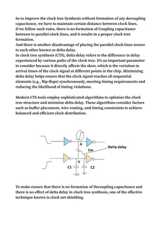
  • 23. So to improve the clock tree Synthesis without formation of any decoupling capacitance, we have to maintain certain distance between clock lines. If we follow such rules, there is no formation of Coupling capacitance between to parallel clock lines, and it results in a proper clock tree formation. And there is another disadvantage of placing the parallel clock lines nearer to each other known as delta delay. In clock tree synthesis (CTS), delta delay refers to the difference in delay experienced by various paths of the clock tree. It's an important parameter to consider because it directly affects the skew, which is the variation in arrival times of the clock signal at different points in the chip. Minimizing delta delay helps ensure that the clock signal reaches all sequential elements (e.g., flip-flops) synchronously, meeting timing requirements and reducing the likelihood of timing violations. Modern CTS tools employ sophisticated algorithms to optimize the clock tree structure and minimize delta delay. These algorithms consider factors such as buffer placement, wire routing, and timing constraints to achieve balanced and efficient clock distribution. To make ensure that there is no formation of Decoupling capacitance and there is no effect of delta delay in clock tree synthesis, one of the effective technique known is clock net shielding.
  • 24. VDD and VSS lines protect the clock signal from coupling and to prevent delta delay. In clock net shielding, the clock signal is shielded by the vdd and vss signal lines that is power and ground lines. The purpose to shield the high speed clock signal is to protect the data paths and clock signals from radiated noise and radiated emissions. After the process of clock net shielding, the layout we can see is as follows:
  • 25. Power Aware CTS: Power-aware Clock Tree Synthesis (CTS) is a technique used in VLSI design to optimize clock distribution networks while considering power consumption as a key design metric. Traditional CTS focuses primarily on minimizing clock skew and improving timing characteristics, but power- aware CTS extends this by also addressing power-related issues. In power-aware CTS, the goal is to design a clock tree that not only meets timing requirements but also minimizes power consumption. We know that, to maintain the signal integrity, we insert buffers in the Clock tree synthesis. In Clock Tree Synthesis (CTS), ensuring balanced loading across the clock tree is fundamental for achieving optimal timing and power characteristics in VLSI designs. The principle of balancing the load at each node and employing identical buffers at each level of the tree serves to maintain consistent signal integrity and minimize skew. Balanced loading ensures that clock signals experience uniform propagation delays as they traverse the tree structure. This balance is essential for meeting setup and hold time requirements across all flip-flops in the design. When every node drives the same load, it helps prevent timing violations by ensuring that clock edges arrive at each flip-flop simultaneously or within the specified timing window.
  • 26. Delay Tables: In Clock Tree Synthesis (CTS), Delay Tables are essential data structures used to characterize the propagation delay of buffers or inverters utilized in the clock tree. These tables provide detailed information about the delay introduced by each buffer or inverter under various operating conditions, such as input slew rates, output loads, and temperature variations. Delay Tables typically consist of a set of delay values corresponding to different input slew rates and output loads. These values are obtained through pre-characterization or simulation of the buffers/inverters under various conditions. Each entry in the table corresponds to the delay introduced by the buffer or inverter for a specific combination of input slew rate and output load. Let us consider the following example By considering the above values and above circuit, consider the delay tables as below:
  • 27. From these Delay tables, we can get the properties of buffers, the capacitive loads, and the delay of the buffers based of the different skew values and output capacitive loads.
  • 28. Static Timing Analysis Static timing analysis (STA) is a critical step in the design and verification of integrated circuits (ICs), particularly in the realm of Very Large-Scale Integration (VLSI) design. STA involves evaluating the timing behavior of digital circuits to ensure that they meet timing requirements specified by the designer. One of the primary objectives of STA is to determine whether the design satisfies setup and hold time constraints for all sequential elements, such as flip-flops or latches, under all possible operating conditions. STA analyzes the timing paths within the design, considering factors such as signal propagation delays, clock skew, and clock uncertainties. By examining these timing paths, STA identifies critical paths with the longest delay, which dictate the maximum achievable clock frequency of the design. STA tools use delay information, typically derived from delay tables or delay models, to perform timing analysis accurately. The results of STA provide designers with insights into the timing performance of their designs, guiding optimization efforts to meet timing constraints and achieve desired performance goals. If there is any violation in the timing or the design doesn’t meet the timing specifications, we have to redesign, resynthesize and modify timing constraints to meet the desired timed requirements. Let’s see some of the timing related terminologies and rules of Static Timing Analysis. Launch Flop & Capture Flop: Launch Flop: A "launch flop" is a flip-flop or latch used to launch a signal or data into a synchronous digital circuit. It is typically associated with the beginning of a timing path. The launch flop receives the data input that needs to be propagated through the digital circuit. Capture Flop: A "capture flop" is a flip-flop or latch used to capture a signal or data at a specific point in a synchronous digital circuit. It is typically associated with the end of a timing path. Upon receiving the clock signal,
  • 29. the capture flop samples and captures the data input at the specific point in time defined by the clock edge Latency time: It is the time taken by the clock signal to travel from the clock source to the destination at the flip flop or It is the arrrival time of a clock signal to flip flop. Source Latency: "Source latency" typically refers to the delay or latency introduced by a source component in a system or process. The source component could be a hardware device, software module, or any other entity responsible for generating data, signals, or events. Network latency: Network latency refers to the time delay that occurs when data packets travel from their source to their destination over a computer network. It is a measure of the time it takes for data to traverse the network between two points and is typically measured in milliseconds (ms) or microseconds (µs).
  • 30. Clock Skew:Clock skew refers to the difference in arrival times of a clock signal at different elements or components of a synchronous digital circuit. Slew:"slew" refers to the rate of change of a signal transition, typically measured as the time it takes for a signal to transition between two logic levels (e.g., from low to high or high to low). It represents how quickly the voltage level of a signal changes over time. Slew rate is usually expressed in terms of voltage change per unit of time, such as volts per nanosecond (V/ns). A high slew rate indicates a fast transition, while a low slew rate indicates a slower transition. Let’s understand the difference between Fast Slew and Slow Slew. Jitter: Jitter is the variation of the
  • 31. clock period from edge to edge It is essentially the deviation from the expected or desired timing of signal events. Jitter can occur in both periodic and aperiodic signals. Clock Uncertainity: Clock uncertainty, also known as clock skew uncertainty or clock timing uncertainty, refers to the variation or uncertainty in the arrival times of clock signals at different components or elements of a digital circuit. It represents the amount of deviation from the ideal arrival times of clock edges specified by the clock period Propagation delay: Propagation delay refers to the time taken for a signal to travel from its source to its destination in a digital circuit. It represents the time delay incurred as a signal propagates through various components of the circuit, such as logic gates, wires, and interconnects
  • 32. Path delay: Path delay, refers to the total time taken for a signal to propagate through a specific path in a digital circuit. It represents the cumulative delay incurred as the signal traverses through various logic gates, interconnects, and other components along the path. Clock-to-Q Delay : The delay associated with the capture of data at flip- flops or latches along the path. This includes the time taken for the output of a flip-flop or latch to become stable after the arrival of the clock signal.
  • 33. Fanout: "Fanout" refers to the number of logic gates or other load components that can be connected to the output of a specific logic gate or driver without causing performance degradation or violating electrical specifications. Let us consider the following example, for the maximum fanout. Critical path: "Critical path" refers to the longest path through a digital circuit from input to output, where the cumulative delay along this path determines the overall timing performance of the circuit. It represents the path that imposes the most significant constraints on the circuit's operational speed and determines the maximum achievable clock frequency. Let’s see an example of about the Critical Path delay.
  • 34. False Path : A "False path" refers to a path in a circuit that is not used to propagate data during normal operation. Despite existing in the design, signals do not flow along a false path during normal operation, either due to conditional logic or because the path is never activated. Multicycle path: A multicycle path, also known as a multicycle constraint, refers to a timing path in a digital circuit where the data does not need to be captured or launched on every clock cycle. Instead, the data may be valid for multiple clock cycles, allowing for a longer timing window for data capture or launch
  • 35. Setup time: Setup time refers to the minimum time duration before the active edge of a clock signal during which the input data signal must remain stable and unchanged for proper capture by a flip-flop or latch in a synchronous digital circuit. In simpler terms, it is the time period prior to the arrival of the clock edge during which the input signal should not change to ensure reliable data capture by the flip-flop or latch Hold time : Hold time refers to the minimum duration after the active edge of a clock signal during which the input data signal must remain stable and unchanged for proper capture by a flip-flop or latch in a synchronous digital circuit. In simpler terms, it is the time period following the arrival of the clock edge during which the input signal should not change to ensure reliable data capture by the flip-flop or latch. Slack: "Slack" refers to the amount of time by which a signal can be delayed without violating timing constraints. A positive slack indicates that the signal has some margin and can be delayed by that amount without causing timing violations. Conversely, a negative slack indicates that the
  • 36. signal is violating timing constraints, and action must be taken to correct the issue, such as optimizing the circuit or adjusting timing constraints. Setup Timing Analysis: The setup timing check can be measured as following for ideal clocks. The setup timing checked always at the next clock edge. Here, for setup timing analysis, the total delay i.e, from clk of launch flop to the capture flop including the combo. Delay must be less than the clock period As we know, in real time, the concept of set up time, clock jitter, clock uncertainty also exists, the timing check for setup can be modified as
  • 37. By considering the real time context, the total delay i.e, from clk of launch flop to the capture flop including the combo. Delay must be less than the clock period by considering the uncertainty and skew. The equation for setup timing analysis is given as follows: (Clk-to-Q)+(Combo.) < (Clock Period)–(Clock Skew)–(Clock Uncertainty) CLK-TO-Q + COMBO < T - S - U In the above equation, CLK-to-Q + COMBO -----> Data Arrival Time T - S - U ------> Data Required Time From the definition, Slack = Data Required Time - Data Arrival Time If slack is positive, that means there are no timing violation in case of setup timing check. If Slack is negative, that means, there is a Setup violation, and we have to optimize the design to discard the violation. For real clocks the buffers are also present in the Clock path. Let’s see an example which considers the setup timing check with real clocks. While considering the real clocks, the delay of buffers is also considered as a part of the Clock Time period and as well as in Arrival time.
  • 38. Hold timing Analysis: The setup timing check can be measured as following for ideal clocks. The setup timing checked always at the same clock edge. Here, for setup timing analysis, the total delay i.e, from clk of launch flop to the capture flop including the combo. Delay must be less than the Hold time. As we know, in real time i.e., for real clocks, the concept of Hold uncertainty, buffer delays are also considered. So the timing check for Hold can be modified as..
  • 39. The equation Hold time analysis is given by, (Clk-to-Q)+(Combo.) > (Hold Time) + (Hold Uncertainty) CLK-TO-Q + COMBO > H + HU In the above equation, CLK-to-Q + COMBO -----> Data Arrival Time H + HU ------> Data Required Time From the definition, Slack = Data Arrival Time - Data Required Time In Static timing Analysis, the Skew is very imporant. In ideal, the design should be designed in such a way that the Skew must be minimized to Zero. But in practical case, it is not possible, we have to minimize the Skew nearer to 0. Possible ways to improve the Set up violations. 1. Gate sizing and Insertion 2. Clock gating 3. Timing Constraints Optimization 4. Adjust Clock timing 5. Buffer Insertion 6. Optimize timing paths Possible ways to improve the Hold vioaltion: 1. Clock Gating 2. Library cell replacement 3. Gate sizing 4. Clock tree synthesis 5. Buffer Insertion
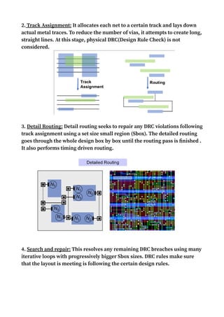
  • 40. ROUTING Routing in VLSI is making physical connections between signal pins using metal layers. Following Clock Tree Synthesis (CTS) and optimization, the routing step determines the exact pathways for interconnecting standard cells, macros, and I/O pins. Steps in Routing : Each metal layer in a grid based routing system has its tracks and preferred routing direction, which are described in a unified cell in the standard cell library. Routing activities are divided into four steps: 1. Global Routing 2. Track assignment 3. Detail Routing 4. Search and repair 1. Global Routing: Global route assigns nets to particular metal layers and global routing cells. The global route aims to avoid crowded global cells while making as few diversions as possible. Global routes also avoid pre- routed P/G, placement, and routing bottlenecks.
  • 41. 2. Track Assignment: It allocates each net to a certain track and lays down actual metal traces. To reduce the number of vias, it attempts to create long, straight lines. At this stage, physical DRC(Design Rule Check) is not considered. 3. Detail Routing: Detail routing seeks to repair any DRC violations following track assignment using a set size small region (Sbox). The detailed routing goes through the whole design box by box until the routing pass is finished . It also performs timing driven routing. 4. Search and repair: This resolves any remaining DRC breaches using many iterative loops with progressively bigger Sbox sizes. DRC rules make sure that the layout is meeting is following the certain design rules.
  • 42. Below is the Part of a real chip viewed by an electron microscope (with artificial colors). In the below diagram, we can see that the wires and pins are on lower planes connected by vias (light blue) Let us consider the below layout which had crossed the design steps of Floorplanning , placement, Clock tree synthesis, Static timing analysis. There are so many algorithms that are followed in routing process. One of such algorithm is Lee’s algorithm used in the purpose of Maze routing. This algorithm is also known as Maze routing Lee’s algorithm. Lee algorithm searches for the shortest path between two terminals and guarantees to find a route between two points if the connection exists. This algorithm represents the routing layer as a grid as shown below
  • 43. This algorithm will be followed by selecting the adjacent cells of every cell excepting the diagonal cells. It is shown below. The process will continue until the destination is reached and then the the routing happens as shown below.
  • 44. Now will get the routed layout, and after that, as a part of routing process, DRC cleaning process will takes place which ensures, whether the layout follows all specified DRC rules. There are so many design rules that should be followed as a part of routing process. Also, there are some typical rules, that should must follow while routing is going on. 1. Wire width 2. Wire pitch 3. Wire spacing 4. Via width 5. Via spacing These all are mentioned below: 1. Wire width: In vlsi fabrication, photolithography technique is used to form the metal connections. This technique used light to make metal connections.As light have a minimum wavelength, using it, we can make minimum width of metal connections. It means the optical wavelength of light can make metal connections. 2. Wire pitch: As per DRC, there is another rule for wire pitch and it should be maintained ,minimum. We have to optimize the layout, to maintain a minimum pitch.
  • 45. 3. Wire spacing: The wire spacing between two data paths, or critical paths, should be maintained and it should not go below the minimum limit. As we know that if we make interconnections, by violating the minimum wire pitch rule, it may results in the formation of coupling capacitance, and may results in crosstalk issues and Signal integrity issues So, it it is important to maintain a minimum distance. For this kind of problem, it is not possible, to shield the data path, to prevent it form crosstalk issues. As net shielding is a difficult task, it is only applicable to critical paths in a layout, like high speed clock signals or some critical data paths. 4. Via width:(Via – The dip of a whoel between ywo or more metal layers used to connnect layers.) The DRC rule specify the via width should be minimum., It can be more, but it can’t be minimum to violate DRC rules. 5. Via spacing:The DRC rule specifies that the minimum spacing between two vias is maintained. They should be at any maximum distance, but min distance is maintained, to make ensure the drc is not violated.
  • 46. -->Major problems in routing arrives when interconects are formed between the routes, so we have to avoid such DRC violations. Parasitic Extraction: After the DRC checking, the next step is parasitic extraction. Parasitic extraction is a vital process in integrated circuit (IC) design, focusing on identifying and characterizing unintended electrical effects known as parasitics. These effects, including resistance, capacitance, Every net has its own resistance and capacitance, so parasitic extraction refers to the extraction of these parameters and make ensure whether the properties doesn’t violate any required parameters in physical design.
  • 47. Capacitance and Resistance of interconnects, known as nets, significantly influence the performance and behavior of integrated circuits. Capacitance directly impacts signal propagation delay along interconnects, contributing to the RC time constant. Higher capacitance leads to longer delays, affecting circuit speed. Additionally, high capacitance can cause signal integrity issues such as distortion, ringing, and crosstalk, potentially compromising the reliability of the circuit. Furthermore, capacitance between nets results in dynamic power consumption during charging and discharging cycles. Resistance also plays a critical role, contributing to the RC time constant along with capacitance. Increased resistance prolongs signal propagation delay and can lead to voltage droop, especially in lengthy interconnects or high-current paths.
  • 48. Sign off: Now, There are some other steps as a part of Sign Off process. These are some verification processes like Design Rule check(DRC) and Layout Vs Schematic(LVS). Design Rule Check(DRC) : Design Rule Checking (DRC) is a pivotal step in the VLSI design workflow, tasked with verifying that the layout adheres rigorously to the specifications and constraints dictated by the fabrication technology. At its core, DRC scrutinizes the geometric aspects of the layout against a predefined set of rules, encompassing parameters like minimum feature size, spacing, width, overlap, and alignment. These rules are intricately tied to the specific fabrication process and technology node being utilized, with semiconductor foundries furnishing designers with a comprehensive set of guidelines to ensure manufacturability and yield. DRC operates across multiple levels of design hierarchy, encompassing cell, block, and chip levels, to ensure compliance at both component and overall layout levels. Layout Vs Schematic(LVS) :
  • 49. Layout vs. Schematic (LVS) verification is an indispensable phase in VLSI design, ensuring the harmony between the physical layout and its schematic representation. LVS scrutinizes the geometric layout of components, such as transistors and interconnects, against the schematic netlist derived from the design specifications. This comparison serves to validate the connectivity between nodes in the layout and their counterparts in the schematic, guaranteeing that electrical connections are accurately depicted in both representations. Moreover, LVS meticulously checks device parameters like size, placement, and orientation to confirm alignment with the schematic's specifications, ensuring consistency in device sizing and placement. After all the verifications done, the final step is to send the chip for fbrication. For that, the GDSII file is sent to fabrication unit to get the chip manufacture.
  • 50. GDSII: A GDSII (Graphical Data System II) file, also known as stream format, is a standard file format used in the semiconductor industry for exchanging information related to the layout of integrated circuits. A GDSII file typically contains the following components: Structures and Layers: GDSII files store geometric shapes and structures representing the layout of an integrated circuit. These structures include polygons, paths, rectangles, circles, and text labels. Each structure is assigned to a specific layer, which defines its purpose or function within the layout hierarchy. Heirarchical Information: GDSII supports hierarchical design, allowing complex layouts to be organized into a hierarchical structure. Each level of hierarchy may contain subcells, which can in turn contain additional subcells, forming a hierarchical tree structure. Cell References: GDSII files include references to cells or instances placed within the layout. These references specify the location, orientation, and scaling of the instances relative to their parent cells DRC Rules and Parameters: Some GDSII files may include design rule information, such as minimum feature size, spacing rules, and other constraints imposed by the semiconductor fabrication process. These rules help ensure that the layout adheres to the requirements of the manufacturing technology.