SlideShare a Scribd company logo
AMITY UNIVERSITY
Rajasthan
VLSI LAB REPORT
SUBMITTED TO
Mr.Venkatrao Selamneni
SUBMITTED BY
Priya Hada
B.tech(ECE)6th
sem
April 28, 2014
Contents
1 INTRODUCTION TO VLSI 1
2 EXPERIMENT NO.1(a) 3
3 EXPERIMENT NO.1(b) 6
4 EXPERIMENT NO.2 10
5 EXPERIMENT NO.3 14
6 EXPERIMENT NO.4 17
7 EXPERIMENT NO.5(a) 20
8 EXPERIMENT NO.5(b) 23
9 EXPERIMENT NO.6(a) 26
10 EXPERIMENT NO.6(b) 29
11 EXPERIMENT NO.7 32
12 EXPERIMENT NO.8 36
13 EXPERIMENT NO.9 40
i
List of Figures
1 Schematic of NMOS . . . . . . . . . . . . . . . . . . . . . . . 4
2 Waveform of NMOS . . . . . . . . . . . . . . . . . . . . . . . 5
3 Schematic of PMOS . . . . . . . . . . . . . . . . . . . . . . . 8
4 Waveform of PMOS . . . . . . . . . . . . . . . . . . . . . . . 9
5 Inverter truth table . . . . . . . . . . . . . . . . . . . . . . . . . 10
6 CMOS inverter . . . . . . . . . . . . . . . . . . . . . . . . . . 10
7 DC characteristics of CMOS inverter . . . . . . . . . . . . . . . 11
8 Schematic of CMOS inverter . . . . . . . . . . . . . . . . . . . 12
9 DC characteristic waveform of CMOS inverter . . . . . . . . . 13
10 Transient characteristics of CMOS inverter with pulse input. . . 14
11 Schematic of CMOS inverter . . . . . . . . . . . . . . . . . . . 15
12 Waveform of CMOS inverter . . . . . . . . . . . . . . . . . . . 16
13 propagation delay graph . . . . . . . . . . . . . . . . . . . . . 17
14 Schematic of CMOS inverter . . . . . . . . . . . . . . . . . . . 18
15 Waveform of CMOS inverter . . . . . . . . . . . . . . . . . . . 19
16 NOR Gate and its truth table . . . . . . . . . . . . . . . . . . . 20
17 Schematic of NOR Gate . . . . . . . . . . . . . . . . . . . . . 21
18 Symbol of NOR Gate . . . . . . . . . . . . . . . . . . . . . . . 21
19 Waveform of NOR Gate . . . . . . . . . . . . . . . . . . . . . 22
20 NAND gate using CMOS logic and its truth table . . . . . . . . 23
21 Schematic of NAND Gate . . . . . . . . . . . . . . . . . . . . 24
22 Waveform of NAND Gate . . . . . . . . . . . . . . . . . . . . 25
23 XOR Gate and its truth table . . . . . . . . . . . . . . . . . . . 26
24 Schematic of XOR Gate . . . . . . . . . . . . . . . . . . . . . 27
25 Waveform of XOR Gate . . . . . . . . . . . . . . . . . . . . . 28
26 XNOR Gate and its truth table . . . . . . . . . . . . . . . . . . 29
27 Schematic of XNOR Gate . . . . . . . . . . . . . . . . . . . . 30
28 Waveform of XNOR Gate . . . . . . . . . . . . . . . . . . . . 31
29 Two input AND gate with truth table . . . . . . . . . . . . . . . 32
ii
30 AND gate using CMOS . . . . . . . . . . . . . . . . . . . . . 33
31 Schematic of NAND gate . . . . . . . . . . . . . . . . . . . . . 33
32 Schematic of NOT gate . . . . . . . . . . . . . . . . . . . . . . 34
33 Schematic of AND gate . . . . . . . . . . . . . . . . . . . . . . 35
34 SR latch diagram with Function Table . . . . . . . . . . . . . . 36
35 Schematic of NAND Gate . . . . . . . . . . . . . . . . . . . . 37
36 Schematic of Symbol of NAND Gate . . . . . . . . . . . . . . . 37
37 Waveform of NAND Gate . . . . . . . . . . . . . . . . . . . . 38
38 Schematic of SR Latch . . . . . . . . . . . . . . . . . . . . . . 38
39 Waveform of SR latch . . . . . . . . . . . . . . . . . . . . . . . 39
40 Symbol and Truthtable of D flipflop . . . . . . . . . . . . . . . 40
41 Schematic D flipflop . . . . . . . . . . . . . . . . . . . . . . . 41
42 Waveform of D flipflop . . . . . . . . . . . . . . . . . . . . . . 42
iii
1 INTRODUCTION TO VLSI
Very-large-scale integration (VLSI) is the process of creating integrated circuits
by combining thousands of transistors into a single chip. Since the invention
of the first Integrated Circuit(IC) by Jack Kilby in 1958, ability to pack more
and more transistors onto a single chip has been very rapid. In the early 1960s,
low density fabrication processes classified under Small Scale Integration (SSI)
in which transistor count was limited to about 10. This rapidly gave way to
Medium Scale Integration (MSI) later in the decade, when around 100 transis-
tors could be placed on a single chip. Early 1970s saw the growth of transistor
count to about 1000 per chip called the Large Scale Integration (LSI).
By mid-1980, the transistor count on a single chip exceeded 1000 and hence
came the age of Very Large Scale Integration or VLSI, which is large scale
integration with a single chip of size as small as 50 millimeters square having
more than a million transistor and circuits in it.
VLSI chiefly comprises of front end design and back end design. While
front end design includes digital design using HDL, design verification through
simulation and other verification techniques, the design from gates and design
for testability, backend design comprises of complementary metal-oxide semi-
conductor (CMOS) design and its characterization.The entire VLSI circuit de-
sign procedure follows a step by step approach, where each design step is fol-
lowed by simulation before it’s put into the hardware. Most VLSI designs are
classified into three Categories:
1. Analog: Small transistor count precision circuits such as Amplifiers, Data
converters, filters, Phase Locked Loops, Sensors etc.
2. Application Specific Integrated Circuits (ASICS): Progress in the fabri-
cation of internal circuits has enabled faster and more powerful circuits in
smaller and smaller devices. ASICS are created for specific purposes and
each device is created to do a particular job, and do it well.
3. Systems on a Chip (SoC): These are highly complex mixed signal circuits,
such as a network processor chip or a wireless radio chip.
Advantages offered by VLSI:
1. Integration improves the design
2. Compactness: less area, physically smaller.
3. Higher speed: lower parasitics(reduced interconnection length).
1
4. Lower power consumption.
5. Higher reliability: improved on-chip interconnects.
6. Integration significantly reduces manufacturing cost.
2
2 EXPERIMENT NO.1(a)
AIM
Study the drain and transfer characteristics of NMOS.
SOFTWARE REQUIRED
Design Architect Tool by Mentor Graphics, LINUX operating system.
THEORY
MOSFET is a four terminal device. The voltage applied to the gate terminal de-
termines if and how much current flows between the source and the drain ports.
The body represents the fourth terminal of the transistor. Its function is sec-
ondary as it only serves to modulate the device characteristics and parameters.
In N-type MOSFET (NMOS), the body is of p-type. The drain, the source and
the channel between the two are of n-type.
Working of NMOS
Initially, VGS = 0, i.e. when no gate to source voltage is applied, it is similar
to two diodes connected back to back between the source and the drain. So,
no current flows from source to drain. Also, a depletion layer is formed at the
source-substrate and the drain-substrate junctions. The holes under the gate are
repelled to produce a depletion region and it becomes continuous.
The VGS is then increased above the Threshold Voltage. At this time, minor-
ity carriers in p-type substrate (electrons) cross the depletion region and reaches
under the gate. The process is called surface inversion.
Modes of operation
It has three modes of operation:
1. Cut-off mode: When no current flows through transistor i.e. ID = 0
occurs when
VGS < VTH
Where VGS: gate to source voltage ; VTH: threshold voltage
3
2. Triode Region: It is a linear region in graph which obeys Ohms law. It
occurs when
VGS > VTH
and
VDS < VGS − VTH
The current equation in triode mode is given as:
ID =
W
L
.µn.Cox(VGS − VTH −
VDS
2
).VDS
3. Saturation Mode: When current becomes constant i.e. ID remains con-
stant no matter how much we increase VGS. It occurs when
VGS > VTH
and
VDS > VGS − VTH
The current equation in saturation mode is given as:
ID =
W
2L
.µn.Cox.(VGS − VTH)2
(1 + λp.VDS)
Where : modulation index
Schematic
Figure 1: Schematic of NMOS
4
Waveforms
Figure 2: Waveform of NMOS
Result
In V I characteristics of NMOS, we observe that at constant VGS if the value of
VDS will increase, then the drain current is saturated.
5
3 EXPERIMENT NO.1(b)
AIM
To study the drain and transfer characteristics of PMOS.
SOFTWARE REQUIRED
Design Architect Tool by Mentor Graphics, LINUX operating system.
THEORY
The structure and operation of a PMOS device is essentially the same, except
that wherever there was n-type silicon, there is now p-type silicon. The PMOS
channel is a part of n-type substrate lying between two heavily doped p+ wells
beneath the source and drain.
Working of PMOS
The operation of PMOS is similar to NMOS. To create an inversion layer in the
n-type substrate, holes have to be attracted to the gate. As a result, p-type chan-
nel will induce between drain and source, the voltage VTH must be sufficiently
negative. The VTH is thus negative, so, channel is induced only if VGS < VTH If
we make the voltage VDS sufficiently negative, the p-type induced channel will
pinch-off. When VDS will be negative, the drain current will flow from source
to drain, exactly opposite to that of NMOS device with a positive VDS .
Modes of Operation
It has three modes of operation -
1. Cut-off mode: It is a mode in which channel is not formed and no current
flows through transistor i.e. ID = 0. It occurs when
VGS > VTH
Where VGS: gate to source voltage, VTH: threshold voltage.
6
2. Linear/Triode region: It is a mode in which channel formation takes place
and thus, current flows from source to drain. This region of graph follows
Ohms law due to linear relationship between IDS and VDS. It occurs when
VGS < VTH
and
VDS > VGS − VTH
The current equation in triode mode is given as:
ID = −
W
L
.µn.Cox(VGS − VTH −
VDS
2
).VDS
3. Saturation mode: In this mode the channel pinches off and the VDSat
which the current saturation occurs is called VDSat or pinch-off voltage.
In this mode the PMOS acts similar to current source.ID is independent
of VDS. It occurs when
VGS < VTH
and
VDS < VGS − VTH
The current equation in saturation mode is given as:
ID = −
W
2L
.µn.Cox.(VGS − VTH)2
(1 + λp.VDS)
Where λp: modulation index
7
Schematic
Figure 3: Schematic of PMOS
8
Waveforms
Figure 4: Waveform of PMOS
Result
The characteristics of PMOS are obtained. All the parameters(voltages and
current) are taken in negative side.
9
4 EXPERIMENT NO.2
AIM
To study D.C. analysis of CMOS inverter.
SOFTWARE REQUIRED
Design Architect Tool by Mentor Graphics, LINUX operating system.
THEORY
Figure 5: Inverter truth table
Figure 6: CMOS inverter
The inverter is universally accepted as the most basic logic gate doing a
Boolean operation on a single input variable.As shown, the simple structure
consists of a combination of an PMOS transistor at the top and a NMOS tran-
sistor at the bottom. CMOS is referred to as complementary-symmetry metalox-
idesemiconductor. The words ”complementary-symmetry” refer to the fact that
the typical digital design style with CMOS uses complementary and symmetri-
cal pairs of p-type and n-type metal oxide semiconductor field effect transistors
10
(MOSFETs) for logic functions. Two important characteristics of CMOS de-
vices are high noise immunity and low static power consumption. Significant
power is only drawn while the transistors in the CMOS device are switching be-
tween on and off states. Consequently, CMOS devices do not produce as much
waste heat as other forms of logic.
DC analysis of CMOS inverter
Figure 7: DC characteristics of CMOS inverter
As shown in above figure there are 5 regions of operation which are sum-
marized as in the table:
11
Schematic
Figure 8: Schematic of CMOS inverter
12
Waveforms
Figure 9: DC characteristic waveform of CMOS inverter
RESULT
The DC characteristic of CMOS inverter is obtained successfully.
13
5 EXPERIMENT NO.3
AIM
To study transient analysis of CMOS inverter.
SOFTWARE REQUIRED
Design Architect Tool by Mentor Graphics, LINUX operating system.
THEORY
Figure 10: Transient characteristics of CMOS inverter with pulse input.
Transient analysis tells Vout(t) if Vin(t) changes. It requires solving differ-
ential equations. Input is usually considered to be a pulse stream.. It is also
called AC analysis or dynamic analysis or switching analysis.The switching
characteristic (Vout(t) given Vin(t)) of a logic gate tells the speed at which the
gate can operate. The switching speed of a logic gate can be measured in terms
of the time required to charge and discharge a capacitive load. Fig.1 shows the
dynamic characteristics of a CMOS inverter. The following are some formal
definitions of temporal parameters of digital circuits. All percentages are of the
steady state values.
1. Rise Time (tr) : Time taken to rise from 10% to 90%
14
2. Fall Time (tf ): Time taken to fall from 90% to 10%
3. Edge Rate (trf ): (tr + tf )/2.
4. High-to-Low propagation delay (tpHL): Time taken to fall from VOH to
50%.
5. Low-to-High propagation delay (tpLH): Time taken to rise from 50% to
VOL.
6. Propagation Delay (tp): (tpHL + tpLH)/2.
7. Contamination Delay (tcd): Minimum time from the input crossing 50%
to the output crossing 50%.
Schematic
Figure 11: Schematic of CMOS inverter
15
Waveforms
Figure 12: Waveform of CMOS inverter
RESULT
The transient characteristics of the CMOS inverter using pulse input is obtained
successfully.
16
6 EXPERIMENT NO.4
AIM
Calculate Rise time, Fall time and Propagation delay of CMOS inverter.
SOFTWARE REQUIRED
Design Architect Tool by Mentor Graphics, LINUX operating system.
THEORY
There are some basic terms that should be known for calculating the transient
parameters of a CMOS inverter. Those are:
1. Switching speed : limited by time taken to charge and discharge, CL .
2. Rise time, tr: Waveform to rise from 10% to 90% of its steady state value
3. Fall time tf , : 90% to 10% of steady state value
4. Delay time, td : time difference between input transition (50%) and 50%
output level
Figure 13: propagation delay graph
The propagation delay tp of a gate defines how quickly it responds to a change at
its inputs, it expresses the delay experienced by a signal when passing through
17
a gate. It is measured between the 50% transition points of the input and output
waveforms as shown in the figure 1 for an inverting gate. The τpLH defines the
response time of the gate for a low to high output transition, while τpHL refers
to a high to low transition. The propagation delay as the average of the two i.e.
tp =
1
2
(τpLH + τpHL)
Schematic
Figure 14: Schematic of CMOS inverter
18
Waveforms
Figure 15: Waveform of CMOS inverter
RESULT
Rise time, Fall time and Propagation delay of CMOS inverter are calculated.
19
7 EXPERIMENT NO.5(a)
AIM
To design two input NOR gate using CMOS logic.
SOFTWARE REQUIRED
Design Architect Tool by Mentor Graphics, LINUX operating system.
THEORY
The NOR gate is a digital logic gate that implements logical NOR. A HIGH
output (1) results if both the inputs to the gate are LOW (0); if one or both input
is HIGH (1), a LOW output (0) results. NOR is the result of the negation of the
OR operator. It can also be seen as an AND gate with all the inputs inverted.
NOR is a functionally complete operationNOR gates can be combined to
generate any other logical function. NOR gates are so-called ”universal gates”
that can be combined to form any other kind of logic gate.
Figure 16: NOR Gate and its truth table
20
Schematic
Figure 17: Schematic of NOR Gate
Symbol
Figure 18: Symbol of NOR Gate
21
Waveforms
Figure 19: Waveform of NOR Gate
RESULT
The wave forms of two input NOR gate are obtained successfully.
22
8 EXPERIMENT NO.5(b)
AIM
To design two input NAND gate using CMOS logic.
SOFTWARE REQUIRED
Design Architect Tool by Mentor Graphics, LINUX operating system.
THEORY
The two-input NAND gate shown in the figure is built from four transistors. The
series-connection of the two n-channel transistors between GND and the gate-
output ensures that the gate-output is only driven low (logical 0) when both
gate inputs a or b are high (logical 1).The complementary parallel connection
of the two transistors between VCC and gate-output means that the gate-output
is driven high (logical 1) when one or both gate inputs are low (logical 0). The
net result is the logical NAND function.
Figure 20: NAND gate using CMOS logic and its truth table
23
Schematic
Figure 21: Schematic of NAND Gate
24
Waveforms
Figure 22: Waveform of NAND Gate
RESULT
The wave forms of two input NAND gate are obtained successfully.
25
9 EXPERIMENT NO.6(a)
AIM
To design two input XOR gate using CMOS logic.
SOFTWARE REQUIRED
Design Architect Tool by Mentor Graphics, LINUX operating system.
THEORY
output is ”true” if either, but not both, of the inputs are ”true.” The output is
”false” if both inputs are ”false” or if both inputs are ”true.” Another way of
looking at this circuit is to observe that the output is 1 if the inputs are different,
but 0 if the inputs are the same. XOR can also be viewed as addition modulo
2. As a result, XOR gates are used to implement binary addition The XOR
( exclusive-OR ) gate acts in the same way as the logical ”either/or.” The in
computers. The algebraic expressions
A.B + A.B
and
(A + B).A.B
both represent the XOR gate with inputs A and B.
Figure 23: XOR Gate and its truth table
26
Schematic
Figure 24: Schematic of XOR Gate
27
Waveforms
Figure 25: Waveform of XOR Gate
RESULT
The wave forms of two input NAND gate are obtained successfully.
28
10 EXPERIMENT NO.6(b)
AIM
To design two input XNOR gate using CMOS logic.
SOFTWARE REQUIRED
Design Architect Tool by Mentor Graphics, LINUX operating system.
THEORY
The XNOR gate (sometimes spelled ”exnor” or ”enor” and rarely written NXOR)
is a digital logic gate whose function is the inverse of the exclusive OR (XOR)
gate. The XNOR (exclusive-NOR) gate is a combination XOR gate followed
by an inverter.
The two-input version implements logical equality. A HIGH output (1) re-
sults if both of the inputs to the gate are the same. If one but not both inputs are
HIGH (1), a LOW output (0) results.
Figure 26: XNOR Gate and its truth table
29
Schematic
Figure 27: Schematic of XNOR Gate
30
Waveforms
Figure 28: Waveform of XNOR Gate
RESULT
The wave forms of two input XNOR gate are obtained successfully.
31
11 EXPERIMENT NO.7
AIM
To design two input AND gate using two input NAND gate and inverter sym-
bols.
SOFTWARE REQUIRED
Design Architect Tool by Mentor Graphics, LINUX operating system.
THEORY
Figure 29: Two input AND gate with truth table
A logic gate is an elementary building block of a digital circuit. A Logic
AND Gate is a type of digital logic gate that has an output which is normally
at logic level 0 and only goes high to a logic level 1 when all of its inputs are
at logic level 1. The output state of a Logic AND Gate only returns low again
when any of its inputs are at a logic level 0. In other words for a logic AND
gate, any low input will give a low output. The logic or Boolean expression
given for a logic AND gate is that for Logical Multiplication which is denoted
by a single dot or full stop symbol,( . ) giving us the Boolean expression of:
A.B = Output
Then we can define the operation of a 2-input logic AND gate as being:
If both A and B are true, then Output is true.
32
Design
For designing two input AND gate with CMOS logic first we have to design
two input NAND gate and its output will be fed to a CMOS inverter to give the
output of AND gate as shown in the figure: Here the output of NAND gate say
Figure 30: AND gate using CMOS
Vz = Vx.Vy Then on passing it through the inverter gives out outputVf = Vx.Vy
which is the expression required for AND gate.
Schematic of NAND
Figure 31: Schematic of NAND gate
33
Schematic of NOT
Figure 32: Schematic of NOT gate
34
Schematic of AND
Figure 33: Schematic of AND gate
RESULT
Two input AND gate using two input NAND gate and Inverter symbols designed
successfully.
35
12 EXPERIMENT NO.8
AIM
To design S-R latch using symbol of NAND gate.
SOFTWARE REQUIRED
Design Architect Tool by Mentor Graphics, LINUX operating system.
THEORY
A latch is a device with exactly two stable states. These states are high-output
and low-output. A latch has a feedback path, so information can be retained by
the device. Therefore latches can be memory devices, and can store one bit of
data for as long as the device is powered. Latches are very similar to flip-flops,
but are not synchronous devices, and do not operate on clock edges as flip-flops
do.
An SR latch (Set/Reset) is an asynchronous device: it works independently
of control signals and relies only on the state of the S and R inputs. SR latches
can be made from NAND gates. In this case, it is sometimes called an SR latch.
Figure 34: SR latch diagram with Function Table
36
Schematic of NAND Gate
Figure 35: Schematic of NAND Gate
Schematic(SYMBOL)
Figure 36: Schematic of Symbol of NAND Gate
37
Waveforms of NAND Gate
Figure 37: Waveform of NAND Gate
Schematic of SR Latch
Figure 38: Schematic of SR Latch
38
Waveforms of SR Latch
Figure 39: Waveform of SR latch
RESULT
S-R latch using symbol of NAND gate designed successfully.
39
13 EXPERIMENT NO.9
AIM
To design D flip flop using CMOS logic.
SOFTWARE REQUIRED
Design Architect Tool by Mentor Graphics, LINUX operating system.
THEORY
The D flip-flop tracks the input, making transitions with match those of the input
D. The D stands for ”data”; this flip-flop stores the value that is on the data line.
It can be thought of as a basic memory cell. A D flip-flop can be made from a
set/reset flip-flop by tying the set to the reset through an inverter. D flip-flops
are by far the most common type of flip-flops and some devices (for example
some FPGAs) are made entirely from D flip-flops. They are also commonly
used for shift-registers and input synchronization.
Figure 40: Symbol and Truthtable of D flipflop
40
Schematic
Figure 41: Schematic D flipflop
41
Waveforms
Figure 42: Waveform of D flipflop
RESULT
D flip flop using CMOS logic obtained successfully.
42

More Related Content

What's hot (20)

PPT
Analog Layout and Process Concern
asinghsaroj
 
PPTX
Electrical outdoor substation
ariramraja1
 
PDF
Fstm deust mip-e141_cee_chap_vi_les diodes
abdennaceur_baghdad
 
PPT
lattice diagram.ppt
krishnakumars92
 
PDF
Get bebas redaman_2014
Abdul Rahman
 
PPSX
analyse numerique
homme00
 
PDF
Channel length Modulation
Engineering Funda
 
PPTX
Short Channel Effect In MOSFET
Sudhanshu Srivastava
 
PDF
Source transformation
Mohankumar Venugopal
 
PDF
Transformer design principles
Leonardo ENERGY
 
PDF
Selective Coordination
michaeljmack
 
PPTX
Low power in vlsi with upf basics part 1
SUNODH GARLAPATI
 
PPSX
Delay Calculation in CMOS Chips Using Logical Effort by Prof. Akhil Masurkar
Akhil Masurkar
 
PPT
Low Power Techniques
keshava murali
 
PPTX
State estimation
Vipin Pandey
 
PDF
Electronique de puissance
badr zaimi
 
PPT
Insulator problems
msmsn2k2
 
PPTX
VLSI Design-Lecture2 introduction to ic technology
sritulasiadigopula
 
PPTX
Pipelining approach
GopinathD17
 
Analog Layout and Process Concern
asinghsaroj
 
Electrical outdoor substation
ariramraja1
 
Fstm deust mip-e141_cee_chap_vi_les diodes
abdennaceur_baghdad
 
lattice diagram.ppt
krishnakumars92
 
Get bebas redaman_2014
Abdul Rahman
 
analyse numerique
homme00
 
Channel length Modulation
Engineering Funda
 
Short Channel Effect In MOSFET
Sudhanshu Srivastava
 
Source transformation
Mohankumar Venugopal
 
Transformer design principles
Leonardo ENERGY
 
Selective Coordination
michaeljmack
 
Low power in vlsi with upf basics part 1
SUNODH GARLAPATI
 
Delay Calculation in CMOS Chips Using Logical Effort by Prof. Akhil Masurkar
Akhil Masurkar
 
Low Power Techniques
keshava murali
 
State estimation
Vipin Pandey
 
Electronique de puissance
badr zaimi
 
Insulator problems
msmsn2k2
 
VLSI Design-Lecture2 introduction to ic technology
sritulasiadigopula
 
Pipelining approach
GopinathD17
 

Viewers also liked (20)

PDF
Plc report with project
Priya Hada
 
PDF
Supply Insensitivity Temperature Sensor for Microprocessor Thermal Monitoring...
IOSR Journals
 
PDF
Vlsi lab manual exp:1
komala vani
 
PDF
Programmable logic-control
akashganesan
 
PPT
Verilogforlab
Shankar Bhukya
 
PDF
Active controls for Flight and Simulation
Stirling Dynamics
 
PDF
Wdm based fso link optimizing for 180 km using bessel filter
eSAT Journals
 
PPTX
PLC Based Paint Mixing Machine
Nikhilesh Vaidya
 
PPTX
Free space optics
Santhoshkumar Yadav
 
PDF
FSO networks under turbulence - Northumbria University 2013 Research Conference
Joaquin Perez
 
PPTX
wireless Communication Underwater(Ocean)
tanveer alam
 
PDF
ESTIMATION OF CHANNEL IN OFDM WIRELESS CHANNEL USING LS AND MMSE TECHNIQUES
IAEME Publication
 
PDF
Introduction to PSPICE
syella
 
PDF
Leos 2008 Th Aa2 20081113 V1.2
jrothim
 
PDF
Types of glasswares
Priya Hada
 
PDF
Free Space Optics
Falak Shah
 
PDF
Plc report
Priya Hada
 
DOCX
Optical Fiber Communication & Bangladesh
Md. Atiqur Rahman
 
PDF
Vlsi design-manual
Ambuj Jha
 
PPTX
unmanned aerial vehicle (UAV)
UDIT PATEL
 
Plc report with project
Priya Hada
 
Supply Insensitivity Temperature Sensor for Microprocessor Thermal Monitoring...
IOSR Journals
 
Vlsi lab manual exp:1
komala vani
 
Programmable logic-control
akashganesan
 
Verilogforlab
Shankar Bhukya
 
Active controls for Flight and Simulation
Stirling Dynamics
 
Wdm based fso link optimizing for 180 km using bessel filter
eSAT Journals
 
PLC Based Paint Mixing Machine
Nikhilesh Vaidya
 
Free space optics
Santhoshkumar Yadav
 
FSO networks under turbulence - Northumbria University 2013 Research Conference
Joaquin Perez
 
wireless Communication Underwater(Ocean)
tanveer alam
 
ESTIMATION OF CHANNEL IN OFDM WIRELESS CHANNEL USING LS AND MMSE TECHNIQUES
IAEME Publication
 
Introduction to PSPICE
syella
 
Leos 2008 Th Aa2 20081113 V1.2
jrothim
 
Types of glasswares
Priya Hada
 
Free Space Optics
Falak Shah
 
Plc report
Priya Hada
 
Optical Fiber Communication & Bangladesh
Md. Atiqur Rahman
 
Vlsi design-manual
Ambuj Jha
 
unmanned aerial vehicle (UAV)
UDIT PATEL
 
Ad

Similar to Vlsi report using latex (20)

PDF
DCMPL_PROJECT_BOOK_SHAY_ITAMAR
shay rubinstain
 
PDF
Digital communication kit
NawfalAhmed1
 
DOCX
VLSI NOTES.docx notes for vlsi ece deptmnt
nitcse
 
PDF
Thesis
Martin Madsen
 
PDF
report
Malik Zaid
 
PDF
Optimization of Threshold Voltage for 65nm PMOS Transistor using Silvaco TCAD...
IOSR Journals
 
PDF
Design of Counter Using SRAM
IOSRJECE
 
PDF
DPRSG IC Design
Rashad Alsaffar
 
PPT
basic_CMOS_technology_CERN_GENEVA_SWITZERLAND.ppt
lefohi9060
 
PDF
Ijetr011811
ER Publication.org
 
PPT
EC6601 VLSI Design CMOS Fabrication
chitrarengasamy
 
PDF
MasterThesis_Bleiker
Simon J. Bleiker
 
PDF
2016 ch4 delay
hdainghia194
 
PDF
Design of two stage OPAMP
Vishal Pathak
 
PDF
EMT529-VLSI-Design-wk1.pdf
Fazrul Faiz Zakaria
 
PDF
High_Voltage_Digital_to_Analog_Converter_thesis
Jeffrey Kittredge, PE
 
PDF
7_DVD_Combinational_MOS_Logic_Circuits.pdf
Usha Mehta
 
PDF
A High Speed Successive Approximation Pipelined ADC.pdf
Kathryn Patel
 
PPT
aet 402 lecture1.ppt vlsi CIRCUIT DESIGN
ATHIRASIVANANDHAN2
 
PDF
A High Speed Successive Approximation Pipelined ADC
Pushpak Dagade
 
DCMPL_PROJECT_BOOK_SHAY_ITAMAR
shay rubinstain
 
Digital communication kit
NawfalAhmed1
 
VLSI NOTES.docx notes for vlsi ece deptmnt
nitcse
 
report
Malik Zaid
 
Optimization of Threshold Voltage for 65nm PMOS Transistor using Silvaco TCAD...
IOSR Journals
 
Design of Counter Using SRAM
IOSRJECE
 
DPRSG IC Design
Rashad Alsaffar
 
basic_CMOS_technology_CERN_GENEVA_SWITZERLAND.ppt
lefohi9060
 
Ijetr011811
ER Publication.org
 
EC6601 VLSI Design CMOS Fabrication
chitrarengasamy
 
MasterThesis_Bleiker
Simon J. Bleiker
 
2016 ch4 delay
hdainghia194
 
Design of two stage OPAMP
Vishal Pathak
 
EMT529-VLSI-Design-wk1.pdf
Fazrul Faiz Zakaria
 
High_Voltage_Digital_to_Analog_Converter_thesis
Jeffrey Kittredge, PE
 
7_DVD_Combinational_MOS_Logic_Circuits.pdf
Usha Mehta
 
A High Speed Successive Approximation Pipelined ADC.pdf
Kathryn Patel
 
aet 402 lecture1.ppt vlsi CIRCUIT DESIGN
ATHIRASIVANANDHAN2
 
A High Speed Successive Approximation Pipelined ADC
Pushpak Dagade
 
Ad

More from Priya Hada (12)

PDF
Plc report
Priya Hada
 
PPTX
Plc and scada theory ppt
Priya Hada
 
PPTX
Plc and scada project ppt
Priya Hada
 
PPTX
Cellular concepts
Priya Hada
 
PDF
Presentation small loop_antennas_electric_field_and_directivity_calculations_...
Priya Hada
 
PPT
Bermuda triangle
Priya Hada
 
DOCX
Final report on line follower
Priya Hada
 
PPTX
Line follower robot
Priya Hada
 
DOCX
## Finalterm paper repport on fso#w245
Priya Hada
 
PPTX
## Final term paper ppt##
Priya Hada
 
PPTX
Emft final pppts
Priya Hada
 
PPT
Priyas final ppts
Priya Hada
 
Plc report
Priya Hada
 
Plc and scada theory ppt
Priya Hada
 
Plc and scada project ppt
Priya Hada
 
Cellular concepts
Priya Hada
 
Presentation small loop_antennas_electric_field_and_directivity_calculations_...
Priya Hada
 
Bermuda triangle
Priya Hada
 
Final report on line follower
Priya Hada
 
Line follower robot
Priya Hada
 
## Finalterm paper repport on fso#w245
Priya Hada
 
## Final term paper ppt##
Priya Hada
 
Emft final pppts
Priya Hada
 
Priyas final ppts
Priya Hada
 

Recently uploaded (20)

PDF
CloudStack GPU Integration - Rohit Yadav
ShapeBlue
 
PPTX
Darren Mills The Migration Modernization Balancing Act: Navigating Risks and...
AWS Chicago
 
PDF
Chris Elwell Woburn, MA - Passionate About IT Innovation
Chris Elwell Woburn, MA
 
PDF
SFWelly Summer 25 Release Highlights July 2025
Anna Loughnan Colquhoun
 
PPTX
MSP360 Backup Scheduling and Retention Best Practices.pptx
MSP360
 
PDF
July Patch Tuesday
Ivanti
 
PDF
TrustArc Webinar - Data Privacy Trends 2025: Mid-Year Insights & Program Stra...
TrustArc
 
PPTX
Webinar: Introduction to LF Energy EVerest
DanBrown980551
 
PPTX
Building and Operating a Private Cloud with CloudStack and LINBIT CloudStack ...
ShapeBlue
 
PDF
Français Patch Tuesday - Juillet
Ivanti
 
PDF
Persuasive AI: risks and opportunities in the age of digital debate
Speck&Tech
 
PDF
Ampere Offers Energy-Efficient Future For AI And Cloud
ShapeBlue
 
PDF
DevBcn - Building 10x Organizations Using Modern Productivity Metrics
Justin Reock
 
PPTX
Top Managed Service Providers in Los Angeles
Captain IT
 
PDF
Apache CloudStack 201: Let's Design & Build an IaaS Cloud
ShapeBlue
 
PDF
Human-centred design in online workplace learning and relationship to engagem...
Tracy Tang
 
PDF
HCIP-Data Center Facility Deployment V2.0 Training Material (Without Remarks ...
mcastillo49
 
PDF
Wojciech Ciemski for Top Cyber News MAGAZINE. June 2025
Dr. Ludmila Morozova-Buss
 
PPTX
Top iOS App Development Company in the USA for Innovative Apps
SynapseIndia
 
PPTX
Building Search Using OpenSearch: Limitations and Workarounds
Sease
 
CloudStack GPU Integration - Rohit Yadav
ShapeBlue
 
Darren Mills The Migration Modernization Balancing Act: Navigating Risks and...
AWS Chicago
 
Chris Elwell Woburn, MA - Passionate About IT Innovation
Chris Elwell Woburn, MA
 
SFWelly Summer 25 Release Highlights July 2025
Anna Loughnan Colquhoun
 
MSP360 Backup Scheduling and Retention Best Practices.pptx
MSP360
 
July Patch Tuesday
Ivanti
 
TrustArc Webinar - Data Privacy Trends 2025: Mid-Year Insights & Program Stra...
TrustArc
 
Webinar: Introduction to LF Energy EVerest
DanBrown980551
 
Building and Operating a Private Cloud with CloudStack and LINBIT CloudStack ...
ShapeBlue
 
Français Patch Tuesday - Juillet
Ivanti
 
Persuasive AI: risks and opportunities in the age of digital debate
Speck&Tech
 
Ampere Offers Energy-Efficient Future For AI And Cloud
ShapeBlue
 
DevBcn - Building 10x Organizations Using Modern Productivity Metrics
Justin Reock
 
Top Managed Service Providers in Los Angeles
Captain IT
 
Apache CloudStack 201: Let's Design & Build an IaaS Cloud
ShapeBlue
 
Human-centred design in online workplace learning and relationship to engagem...
Tracy Tang
 
HCIP-Data Center Facility Deployment V2.0 Training Material (Without Remarks ...
mcastillo49
 
Wojciech Ciemski for Top Cyber News MAGAZINE. June 2025
Dr. Ludmila Morozova-Buss
 
Top iOS App Development Company in the USA for Innovative Apps
SynapseIndia
 
Building Search Using OpenSearch: Limitations and Workarounds
Sease
 

Vlsi report using latex

  • 1. AMITY UNIVERSITY Rajasthan VLSI LAB REPORT SUBMITTED TO Mr.Venkatrao Selamneni SUBMITTED BY Priya Hada B.tech(ECE)6th sem April 28, 2014
  • 2. Contents 1 INTRODUCTION TO VLSI 1 2 EXPERIMENT NO.1(a) 3 3 EXPERIMENT NO.1(b) 6 4 EXPERIMENT NO.2 10 5 EXPERIMENT NO.3 14 6 EXPERIMENT NO.4 17 7 EXPERIMENT NO.5(a) 20 8 EXPERIMENT NO.5(b) 23 9 EXPERIMENT NO.6(a) 26 10 EXPERIMENT NO.6(b) 29 11 EXPERIMENT NO.7 32 12 EXPERIMENT NO.8 36 13 EXPERIMENT NO.9 40 i
  • 3. List of Figures 1 Schematic of NMOS . . . . . . . . . . . . . . . . . . . . . . . 4 2 Waveform of NMOS . . . . . . . . . . . . . . . . . . . . . . . 5 3 Schematic of PMOS . . . . . . . . . . . . . . . . . . . . . . . 8 4 Waveform of PMOS . . . . . . . . . . . . . . . . . . . . . . . 9 5 Inverter truth table . . . . . . . . . . . . . . . . . . . . . . . . . 10 6 CMOS inverter . . . . . . . . . . . . . . . . . . . . . . . . . . 10 7 DC characteristics of CMOS inverter . . . . . . . . . . . . . . . 11 8 Schematic of CMOS inverter . . . . . . . . . . . . . . . . . . . 12 9 DC characteristic waveform of CMOS inverter . . . . . . . . . 13 10 Transient characteristics of CMOS inverter with pulse input. . . 14 11 Schematic of CMOS inverter . . . . . . . . . . . . . . . . . . . 15 12 Waveform of CMOS inverter . . . . . . . . . . . . . . . . . . . 16 13 propagation delay graph . . . . . . . . . . . . . . . . . . . . . 17 14 Schematic of CMOS inverter . . . . . . . . . . . . . . . . . . . 18 15 Waveform of CMOS inverter . . . . . . . . . . . . . . . . . . . 19 16 NOR Gate and its truth table . . . . . . . . . . . . . . . . . . . 20 17 Schematic of NOR Gate . . . . . . . . . . . . . . . . . . . . . 21 18 Symbol of NOR Gate . . . . . . . . . . . . . . . . . . . . . . . 21 19 Waveform of NOR Gate . . . . . . . . . . . . . . . . . . . . . 22 20 NAND gate using CMOS logic and its truth table . . . . . . . . 23 21 Schematic of NAND Gate . . . . . . . . . . . . . . . . . . . . 24 22 Waveform of NAND Gate . . . . . . . . . . . . . . . . . . . . 25 23 XOR Gate and its truth table . . . . . . . . . . . . . . . . . . . 26 24 Schematic of XOR Gate . . . . . . . . . . . . . . . . . . . . . 27 25 Waveform of XOR Gate . . . . . . . . . . . . . . . . . . . . . 28 26 XNOR Gate and its truth table . . . . . . . . . . . . . . . . . . 29 27 Schematic of XNOR Gate . . . . . . . . . . . . . . . . . . . . 30 28 Waveform of XNOR Gate . . . . . . . . . . . . . . . . . . . . 31 29 Two input AND gate with truth table . . . . . . . . . . . . . . . 32 ii
  • 4. 30 AND gate using CMOS . . . . . . . . . . . . . . . . . . . . . 33 31 Schematic of NAND gate . . . . . . . . . . . . . . . . . . . . . 33 32 Schematic of NOT gate . . . . . . . . . . . . . . . . . . . . . . 34 33 Schematic of AND gate . . . . . . . . . . . . . . . . . . . . . . 35 34 SR latch diagram with Function Table . . . . . . . . . . . . . . 36 35 Schematic of NAND Gate . . . . . . . . . . . . . . . . . . . . 37 36 Schematic of Symbol of NAND Gate . . . . . . . . . . . . . . . 37 37 Waveform of NAND Gate . . . . . . . . . . . . . . . . . . . . 38 38 Schematic of SR Latch . . . . . . . . . . . . . . . . . . . . . . 38 39 Waveform of SR latch . . . . . . . . . . . . . . . . . . . . . . . 39 40 Symbol and Truthtable of D flipflop . . . . . . . . . . . . . . . 40 41 Schematic D flipflop . . . . . . . . . . . . . . . . . . . . . . . 41 42 Waveform of D flipflop . . . . . . . . . . . . . . . . . . . . . . 42 iii
  • 5. 1 INTRODUCTION TO VLSI Very-large-scale integration (VLSI) is the process of creating integrated circuits by combining thousands of transistors into a single chip. Since the invention of the first Integrated Circuit(IC) by Jack Kilby in 1958, ability to pack more and more transistors onto a single chip has been very rapid. In the early 1960s, low density fabrication processes classified under Small Scale Integration (SSI) in which transistor count was limited to about 10. This rapidly gave way to Medium Scale Integration (MSI) later in the decade, when around 100 transis- tors could be placed on a single chip. Early 1970s saw the growth of transistor count to about 1000 per chip called the Large Scale Integration (LSI). By mid-1980, the transistor count on a single chip exceeded 1000 and hence came the age of Very Large Scale Integration or VLSI, which is large scale integration with a single chip of size as small as 50 millimeters square having more than a million transistor and circuits in it. VLSI chiefly comprises of front end design and back end design. While front end design includes digital design using HDL, design verification through simulation and other verification techniques, the design from gates and design for testability, backend design comprises of complementary metal-oxide semi- conductor (CMOS) design and its characterization.The entire VLSI circuit de- sign procedure follows a step by step approach, where each design step is fol- lowed by simulation before it’s put into the hardware. Most VLSI designs are classified into three Categories: 1. Analog: Small transistor count precision circuits such as Amplifiers, Data converters, filters, Phase Locked Loops, Sensors etc. 2. Application Specific Integrated Circuits (ASICS): Progress in the fabri- cation of internal circuits has enabled faster and more powerful circuits in smaller and smaller devices. ASICS are created for specific purposes and each device is created to do a particular job, and do it well. 3. Systems on a Chip (SoC): These are highly complex mixed signal circuits, such as a network processor chip or a wireless radio chip. Advantages offered by VLSI: 1. Integration improves the design 2. Compactness: less area, physically smaller. 3. Higher speed: lower parasitics(reduced interconnection length). 1
  • 6. 4. Lower power consumption. 5. Higher reliability: improved on-chip interconnects. 6. Integration significantly reduces manufacturing cost. 2
  • 7. 2 EXPERIMENT NO.1(a) AIM Study the drain and transfer characteristics of NMOS. SOFTWARE REQUIRED Design Architect Tool by Mentor Graphics, LINUX operating system. THEORY MOSFET is a four terminal device. The voltage applied to the gate terminal de- termines if and how much current flows between the source and the drain ports. The body represents the fourth terminal of the transistor. Its function is sec- ondary as it only serves to modulate the device characteristics and parameters. In N-type MOSFET (NMOS), the body is of p-type. The drain, the source and the channel between the two are of n-type. Working of NMOS Initially, VGS = 0, i.e. when no gate to source voltage is applied, it is similar to two diodes connected back to back between the source and the drain. So, no current flows from source to drain. Also, a depletion layer is formed at the source-substrate and the drain-substrate junctions. The holes under the gate are repelled to produce a depletion region and it becomes continuous. The VGS is then increased above the Threshold Voltage. At this time, minor- ity carriers in p-type substrate (electrons) cross the depletion region and reaches under the gate. The process is called surface inversion. Modes of operation It has three modes of operation: 1. Cut-off mode: When no current flows through transistor i.e. ID = 0 occurs when VGS < VTH Where VGS: gate to source voltage ; VTH: threshold voltage 3
  • 8. 2. Triode Region: It is a linear region in graph which obeys Ohms law. It occurs when VGS > VTH and VDS < VGS − VTH The current equation in triode mode is given as: ID = W L .µn.Cox(VGS − VTH − VDS 2 ).VDS 3. Saturation Mode: When current becomes constant i.e. ID remains con- stant no matter how much we increase VGS. It occurs when VGS > VTH and VDS > VGS − VTH The current equation in saturation mode is given as: ID = W 2L .µn.Cox.(VGS − VTH)2 (1 + λp.VDS) Where : modulation index Schematic Figure 1: Schematic of NMOS 4
  • 9. Waveforms Figure 2: Waveform of NMOS Result In V I characteristics of NMOS, we observe that at constant VGS if the value of VDS will increase, then the drain current is saturated. 5
  • 10. 3 EXPERIMENT NO.1(b) AIM To study the drain and transfer characteristics of PMOS. SOFTWARE REQUIRED Design Architect Tool by Mentor Graphics, LINUX operating system. THEORY The structure and operation of a PMOS device is essentially the same, except that wherever there was n-type silicon, there is now p-type silicon. The PMOS channel is a part of n-type substrate lying between two heavily doped p+ wells beneath the source and drain. Working of PMOS The operation of PMOS is similar to NMOS. To create an inversion layer in the n-type substrate, holes have to be attracted to the gate. As a result, p-type chan- nel will induce between drain and source, the voltage VTH must be sufficiently negative. The VTH is thus negative, so, channel is induced only if VGS < VTH If we make the voltage VDS sufficiently negative, the p-type induced channel will pinch-off. When VDS will be negative, the drain current will flow from source to drain, exactly opposite to that of NMOS device with a positive VDS . Modes of Operation It has three modes of operation - 1. Cut-off mode: It is a mode in which channel is not formed and no current flows through transistor i.e. ID = 0. It occurs when VGS > VTH Where VGS: gate to source voltage, VTH: threshold voltage. 6
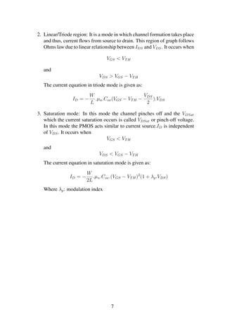
  • 11. 2. Linear/Triode region: It is a mode in which channel formation takes place and thus, current flows from source to drain. This region of graph follows Ohms law due to linear relationship between IDS and VDS. It occurs when VGS < VTH and VDS > VGS − VTH The current equation in triode mode is given as: ID = − W L .µn.Cox(VGS − VTH − VDS 2 ).VDS 3. Saturation mode: In this mode the channel pinches off and the VDSat which the current saturation occurs is called VDSat or pinch-off voltage. In this mode the PMOS acts similar to current source.ID is independent of VDS. It occurs when VGS < VTH and VDS < VGS − VTH The current equation in saturation mode is given as: ID = − W 2L .µn.Cox.(VGS − VTH)2 (1 + λp.VDS) Where λp: modulation index 7
  • 13. Waveforms Figure 4: Waveform of PMOS Result The characteristics of PMOS are obtained. All the parameters(voltages and current) are taken in negative side. 9
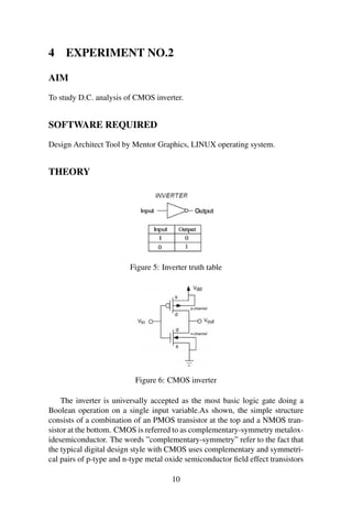
  • 14. 4 EXPERIMENT NO.2 AIM To study D.C. analysis of CMOS inverter. SOFTWARE REQUIRED Design Architect Tool by Mentor Graphics, LINUX operating system. THEORY Figure 5: Inverter truth table Figure 6: CMOS inverter The inverter is universally accepted as the most basic logic gate doing a Boolean operation on a single input variable.As shown, the simple structure consists of a combination of an PMOS transistor at the top and a NMOS tran- sistor at the bottom. CMOS is referred to as complementary-symmetry metalox- idesemiconductor. The words ”complementary-symmetry” refer to the fact that the typical digital design style with CMOS uses complementary and symmetri- cal pairs of p-type and n-type metal oxide semiconductor field effect transistors 10
  • 15. (MOSFETs) for logic functions. Two important characteristics of CMOS de- vices are high noise immunity and low static power consumption. Significant power is only drawn while the transistors in the CMOS device are switching be- tween on and off states. Consequently, CMOS devices do not produce as much waste heat as other forms of logic. DC analysis of CMOS inverter Figure 7: DC characteristics of CMOS inverter As shown in above figure there are 5 regions of operation which are sum- marized as in the table: 11
  • 16. Schematic Figure 8: Schematic of CMOS inverter 12
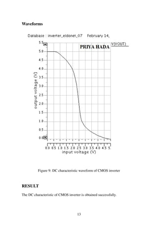
  • 17. Waveforms Figure 9: DC characteristic waveform of CMOS inverter RESULT The DC characteristic of CMOS inverter is obtained successfully. 13
  • 18. 5 EXPERIMENT NO.3 AIM To study transient analysis of CMOS inverter. SOFTWARE REQUIRED Design Architect Tool by Mentor Graphics, LINUX operating system. THEORY Figure 10: Transient characteristics of CMOS inverter with pulse input. Transient analysis tells Vout(t) if Vin(t) changes. It requires solving differ- ential equations. Input is usually considered to be a pulse stream.. It is also called AC analysis or dynamic analysis or switching analysis.The switching characteristic (Vout(t) given Vin(t)) of a logic gate tells the speed at which the gate can operate. The switching speed of a logic gate can be measured in terms of the time required to charge and discharge a capacitive load. Fig.1 shows the dynamic characteristics of a CMOS inverter. The following are some formal definitions of temporal parameters of digital circuits. All percentages are of the steady state values. 1. Rise Time (tr) : Time taken to rise from 10% to 90% 14
  • 19. 2. Fall Time (tf ): Time taken to fall from 90% to 10% 3. Edge Rate (trf ): (tr + tf )/2. 4. High-to-Low propagation delay (tpHL): Time taken to fall from VOH to 50%. 5. Low-to-High propagation delay (tpLH): Time taken to rise from 50% to VOL. 6. Propagation Delay (tp): (tpHL + tpLH)/2. 7. Contamination Delay (tcd): Minimum time from the input crossing 50% to the output crossing 50%. Schematic Figure 11: Schematic of CMOS inverter 15
  • 20. Waveforms Figure 12: Waveform of CMOS inverter RESULT The transient characteristics of the CMOS inverter using pulse input is obtained successfully. 16
  • 21. 6 EXPERIMENT NO.4 AIM Calculate Rise time, Fall time and Propagation delay of CMOS inverter. SOFTWARE REQUIRED Design Architect Tool by Mentor Graphics, LINUX operating system. THEORY There are some basic terms that should be known for calculating the transient parameters of a CMOS inverter. Those are: 1. Switching speed : limited by time taken to charge and discharge, CL . 2. Rise time, tr: Waveform to rise from 10% to 90% of its steady state value 3. Fall time tf , : 90% to 10% of steady state value 4. Delay time, td : time difference between input transition (50%) and 50% output level Figure 13: propagation delay graph The propagation delay tp of a gate defines how quickly it responds to a change at its inputs, it expresses the delay experienced by a signal when passing through 17
  • 22. a gate. It is measured between the 50% transition points of the input and output waveforms as shown in the figure 1 for an inverting gate. The τpLH defines the response time of the gate for a low to high output transition, while τpHL refers to a high to low transition. The propagation delay as the average of the two i.e. tp = 1 2 (τpLH + τpHL) Schematic Figure 14: Schematic of CMOS inverter 18
  • 23. Waveforms Figure 15: Waveform of CMOS inverter RESULT Rise time, Fall time and Propagation delay of CMOS inverter are calculated. 19
  • 24. 7 EXPERIMENT NO.5(a) AIM To design two input NOR gate using CMOS logic. SOFTWARE REQUIRED Design Architect Tool by Mentor Graphics, LINUX operating system. THEORY The NOR gate is a digital logic gate that implements logical NOR. A HIGH output (1) results if both the inputs to the gate are LOW (0); if one or both input is HIGH (1), a LOW output (0) results. NOR is the result of the negation of the OR operator. It can also be seen as an AND gate with all the inputs inverted. NOR is a functionally complete operationNOR gates can be combined to generate any other logical function. NOR gates are so-called ”universal gates” that can be combined to form any other kind of logic gate. Figure 16: NOR Gate and its truth table 20
  • 25. Schematic Figure 17: Schematic of NOR Gate Symbol Figure 18: Symbol of NOR Gate 21
  • 26. Waveforms Figure 19: Waveform of NOR Gate RESULT The wave forms of two input NOR gate are obtained successfully. 22
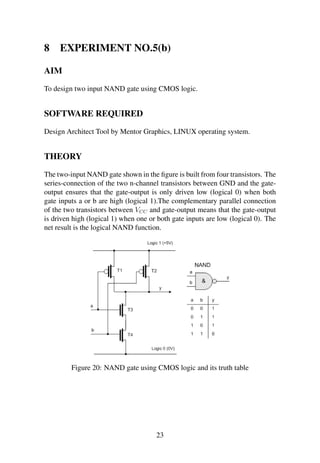
  • 27. 8 EXPERIMENT NO.5(b) AIM To design two input NAND gate using CMOS logic. SOFTWARE REQUIRED Design Architect Tool by Mentor Graphics, LINUX operating system. THEORY The two-input NAND gate shown in the figure is built from four transistors. The series-connection of the two n-channel transistors between GND and the gate- output ensures that the gate-output is only driven low (logical 0) when both gate inputs a or b are high (logical 1).The complementary parallel connection of the two transistors between VCC and gate-output means that the gate-output is driven high (logical 1) when one or both gate inputs are low (logical 0). The net result is the logical NAND function. Figure 20: NAND gate using CMOS logic and its truth table 23
  • 29. Waveforms Figure 22: Waveform of NAND Gate RESULT The wave forms of two input NAND gate are obtained successfully. 25
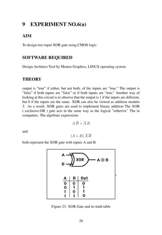
  • 30. 9 EXPERIMENT NO.6(a) AIM To design two input XOR gate using CMOS logic. SOFTWARE REQUIRED Design Architect Tool by Mentor Graphics, LINUX operating system. THEORY output is ”true” if either, but not both, of the inputs are ”true.” The output is ”false” if both inputs are ”false” or if both inputs are ”true.” Another way of looking at this circuit is to observe that the output is 1 if the inputs are different, but 0 if the inputs are the same. XOR can also be viewed as addition modulo 2. As a result, XOR gates are used to implement binary addition The XOR ( exclusive-OR ) gate acts in the same way as the logical ”either/or.” The in computers. The algebraic expressions A.B + A.B and (A + B).A.B both represent the XOR gate with inputs A and B. Figure 23: XOR Gate and its truth table 26
  • 32. Waveforms Figure 25: Waveform of XOR Gate RESULT The wave forms of two input NAND gate are obtained successfully. 28
  • 33. 10 EXPERIMENT NO.6(b) AIM To design two input XNOR gate using CMOS logic. SOFTWARE REQUIRED Design Architect Tool by Mentor Graphics, LINUX operating system. THEORY The XNOR gate (sometimes spelled ”exnor” or ”enor” and rarely written NXOR) is a digital logic gate whose function is the inverse of the exclusive OR (XOR) gate. The XNOR (exclusive-NOR) gate is a combination XOR gate followed by an inverter. The two-input version implements logical equality. A HIGH output (1) re- sults if both of the inputs to the gate are the same. If one but not both inputs are HIGH (1), a LOW output (0) results. Figure 26: XNOR Gate and its truth table 29
  • 35. Waveforms Figure 28: Waveform of XNOR Gate RESULT The wave forms of two input XNOR gate are obtained successfully. 31
  • 36. 11 EXPERIMENT NO.7 AIM To design two input AND gate using two input NAND gate and inverter sym- bols. SOFTWARE REQUIRED Design Architect Tool by Mentor Graphics, LINUX operating system. THEORY Figure 29: Two input AND gate with truth table A logic gate is an elementary building block of a digital circuit. A Logic AND Gate is a type of digital logic gate that has an output which is normally at logic level 0 and only goes high to a logic level 1 when all of its inputs are at logic level 1. The output state of a Logic AND Gate only returns low again when any of its inputs are at a logic level 0. In other words for a logic AND gate, any low input will give a low output. The logic or Boolean expression given for a logic AND gate is that for Logical Multiplication which is denoted by a single dot or full stop symbol,( . ) giving us the Boolean expression of: A.B = Output Then we can define the operation of a 2-input logic AND gate as being: If both A and B are true, then Output is true. 32
  • 37. Design For designing two input AND gate with CMOS logic first we have to design two input NAND gate and its output will be fed to a CMOS inverter to give the output of AND gate as shown in the figure: Here the output of NAND gate say Figure 30: AND gate using CMOS Vz = Vx.Vy Then on passing it through the inverter gives out outputVf = Vx.Vy which is the expression required for AND gate. Schematic of NAND Figure 31: Schematic of NAND gate 33
  • 38. Schematic of NOT Figure 32: Schematic of NOT gate 34
  • 39. Schematic of AND Figure 33: Schematic of AND gate RESULT Two input AND gate using two input NAND gate and Inverter symbols designed successfully. 35
  • 40. 12 EXPERIMENT NO.8 AIM To design S-R latch using symbol of NAND gate. SOFTWARE REQUIRED Design Architect Tool by Mentor Graphics, LINUX operating system. THEORY A latch is a device with exactly two stable states. These states are high-output and low-output. A latch has a feedback path, so information can be retained by the device. Therefore latches can be memory devices, and can store one bit of data for as long as the device is powered. Latches are very similar to flip-flops, but are not synchronous devices, and do not operate on clock edges as flip-flops do. An SR latch (Set/Reset) is an asynchronous device: it works independently of control signals and relies only on the state of the S and R inputs. SR latches can be made from NAND gates. In this case, it is sometimes called an SR latch. Figure 34: SR latch diagram with Function Table 36
  • 41. Schematic of NAND Gate Figure 35: Schematic of NAND Gate Schematic(SYMBOL) Figure 36: Schematic of Symbol of NAND Gate 37
  • 42. Waveforms of NAND Gate Figure 37: Waveform of NAND Gate Schematic of SR Latch Figure 38: Schematic of SR Latch 38
  • 43. Waveforms of SR Latch Figure 39: Waveform of SR latch RESULT S-R latch using symbol of NAND gate designed successfully. 39
  • 44. 13 EXPERIMENT NO.9 AIM To design D flip flop using CMOS logic. SOFTWARE REQUIRED Design Architect Tool by Mentor Graphics, LINUX operating system. THEORY The D flip-flop tracks the input, making transitions with match those of the input D. The D stands for ”data”; this flip-flop stores the value that is on the data line. It can be thought of as a basic memory cell. A D flip-flop can be made from a set/reset flip-flop by tying the set to the reset through an inverter. D flip-flops are by far the most common type of flip-flops and some devices (for example some FPGAs) are made entirely from D flip-flops. They are also commonly used for shift-registers and input synchronization. Figure 40: Symbol and Truthtable of D flipflop 40
  • 46. Waveforms Figure 42: Waveform of D flipflop RESULT D flip flop using CMOS logic obtained successfully. 42